
Modeling and Simulation for Predicting Thermo-Mechanical Behavior of Wafer-Level Cu-PI RDLs During Manufacturing


 ,
,
Abstract
1. Introduction
2. Materials and Methods
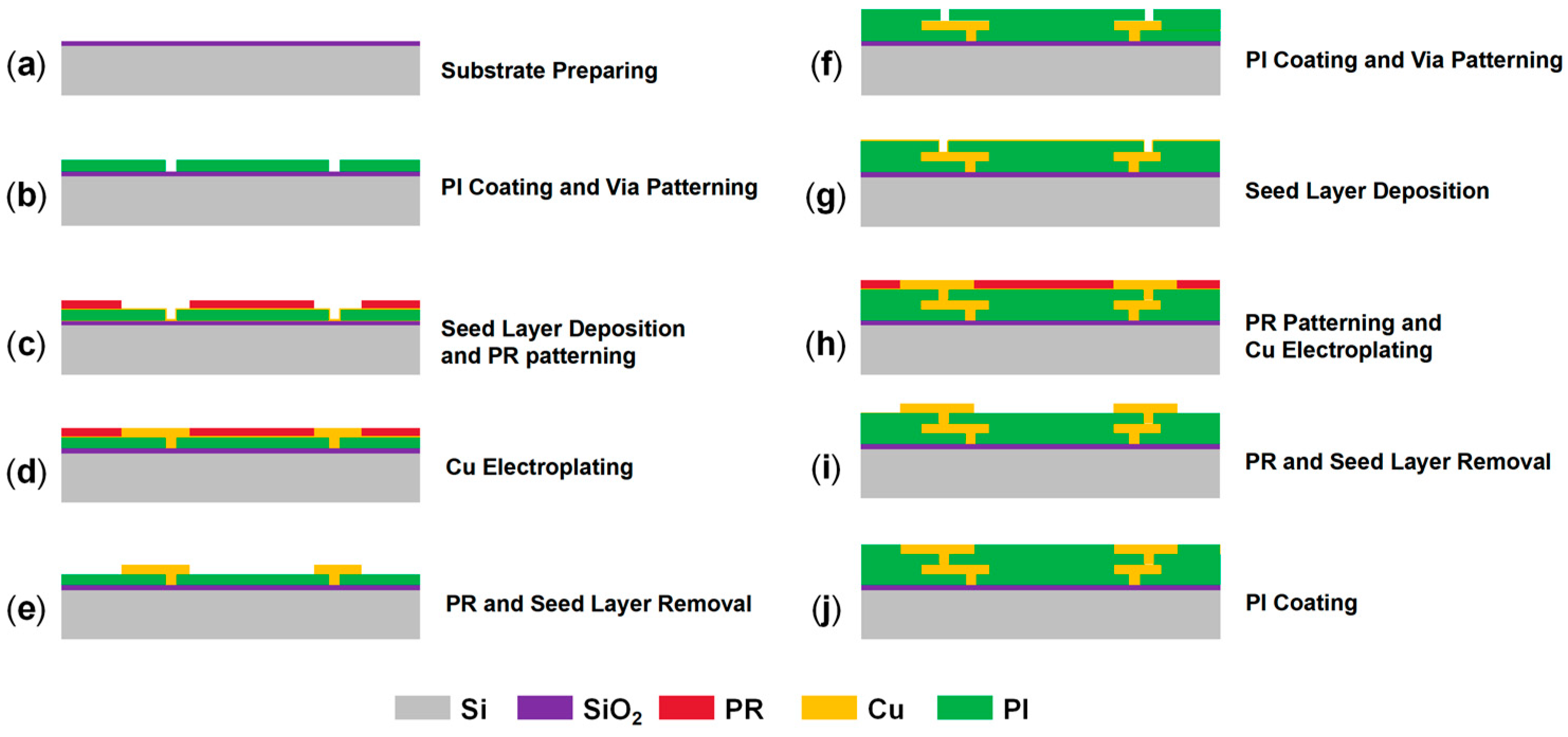
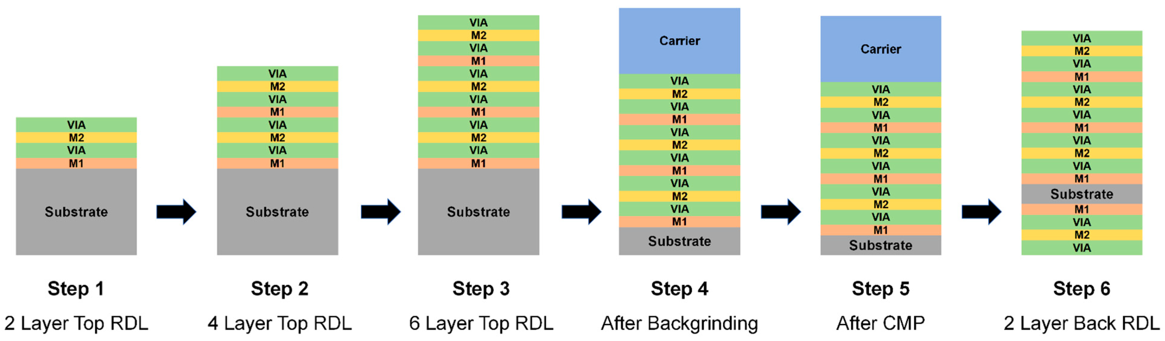
2.1. Structure
2.2. Equivalent Finite Element Model
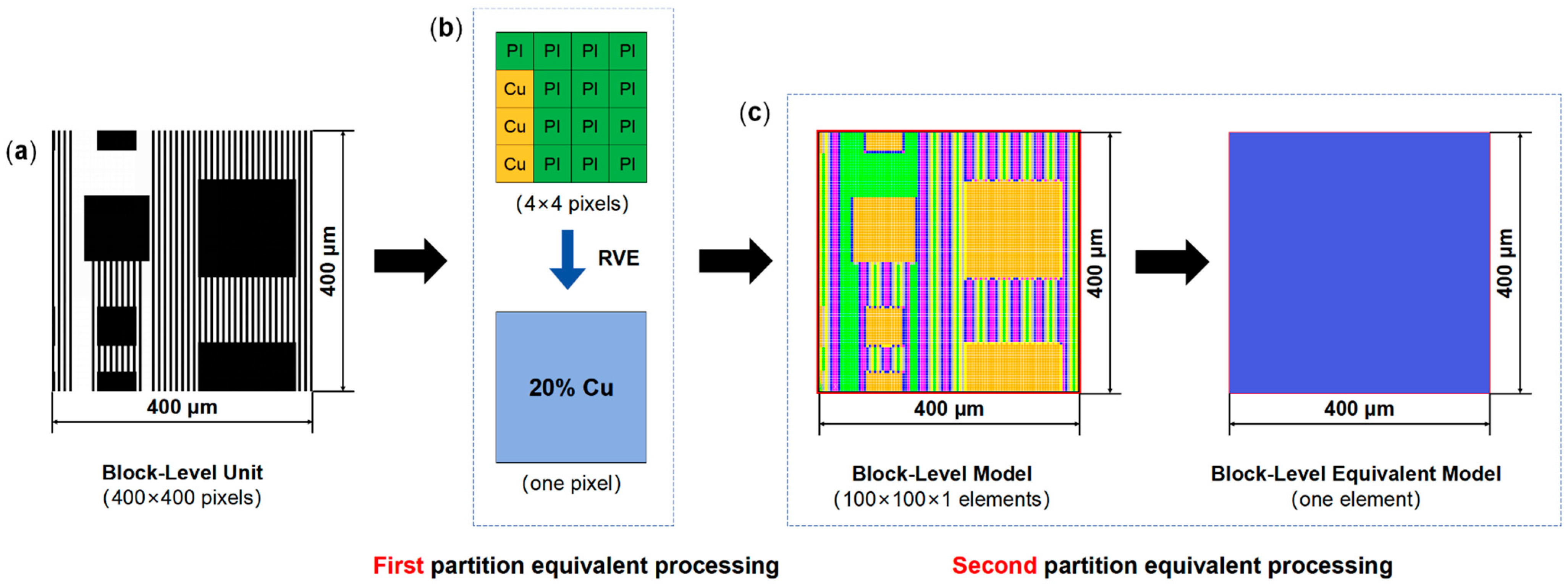
2.2.1. Block-Level Model
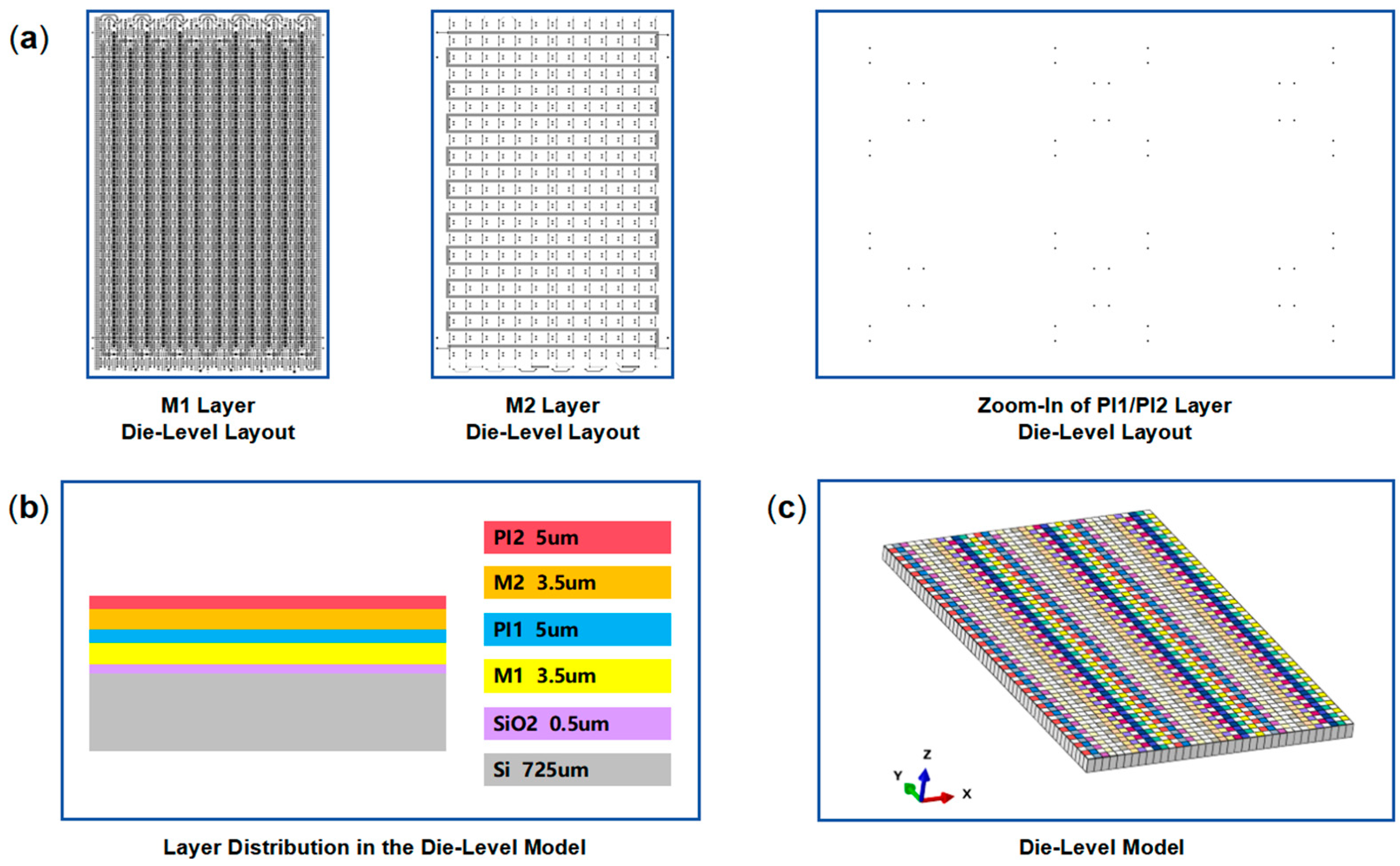
2.2.2. Die-Level Model
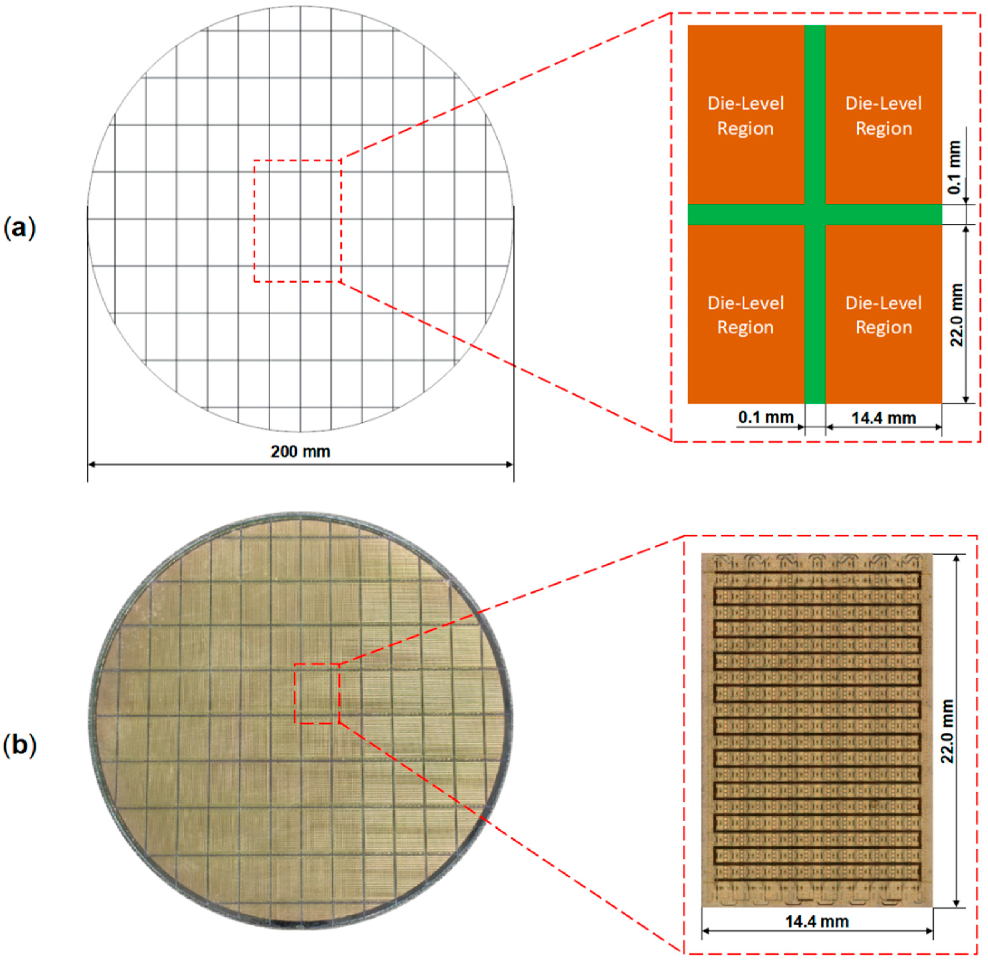
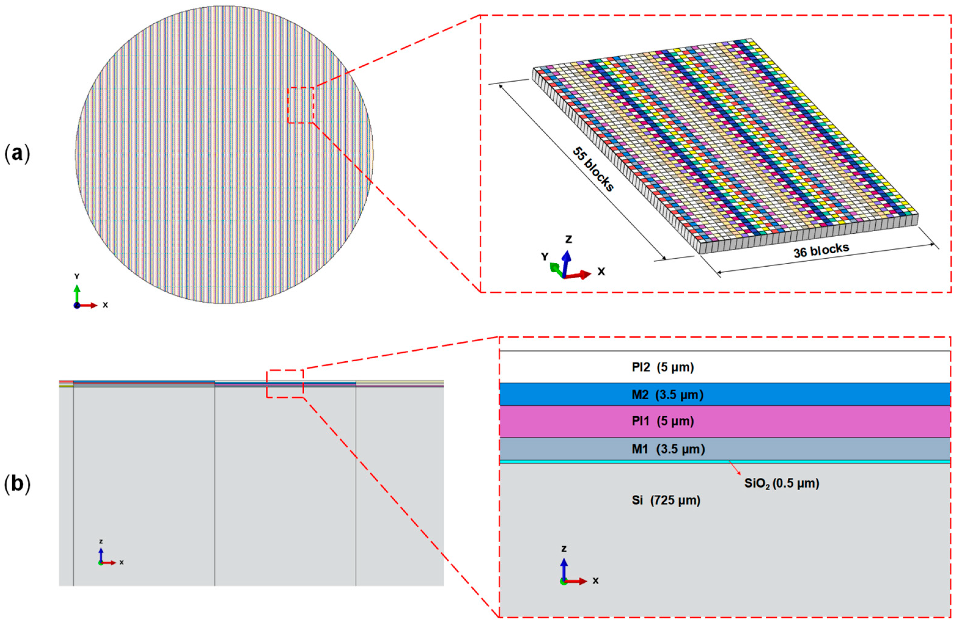
2.2.3. Wafer-Level Model
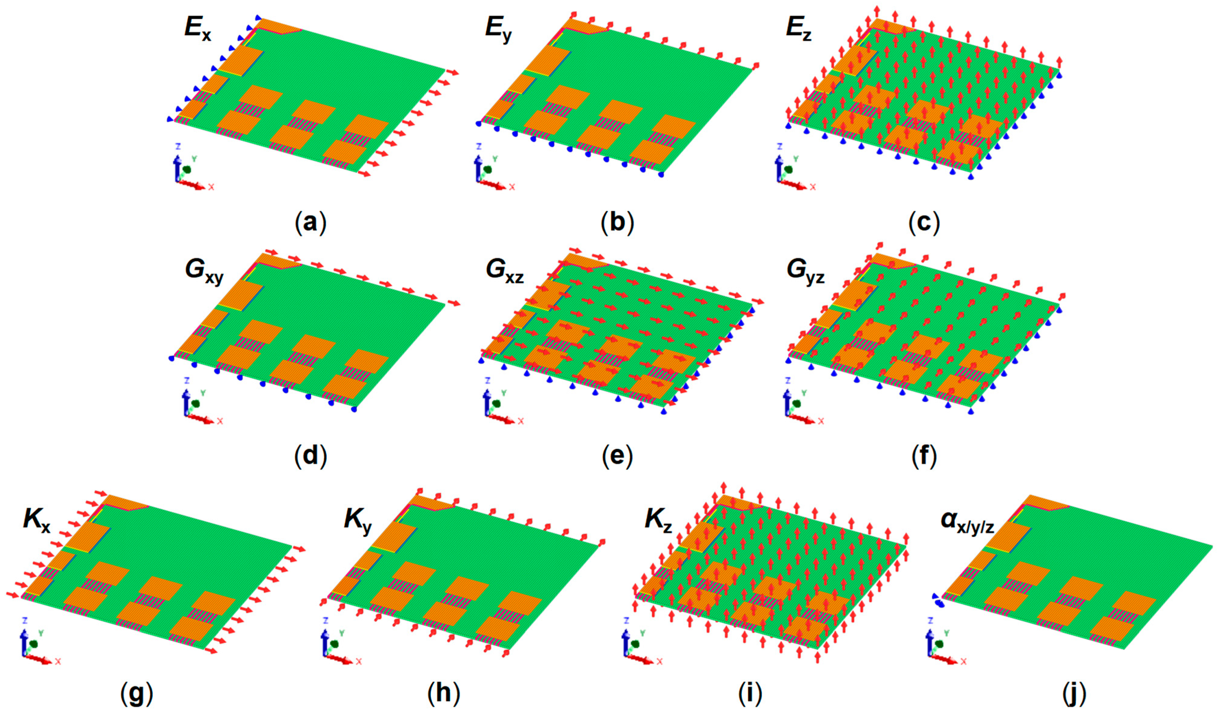
2.3. Boundary Conditions
2.4. Extraction of PI Material Properties
3. Results and Discussion
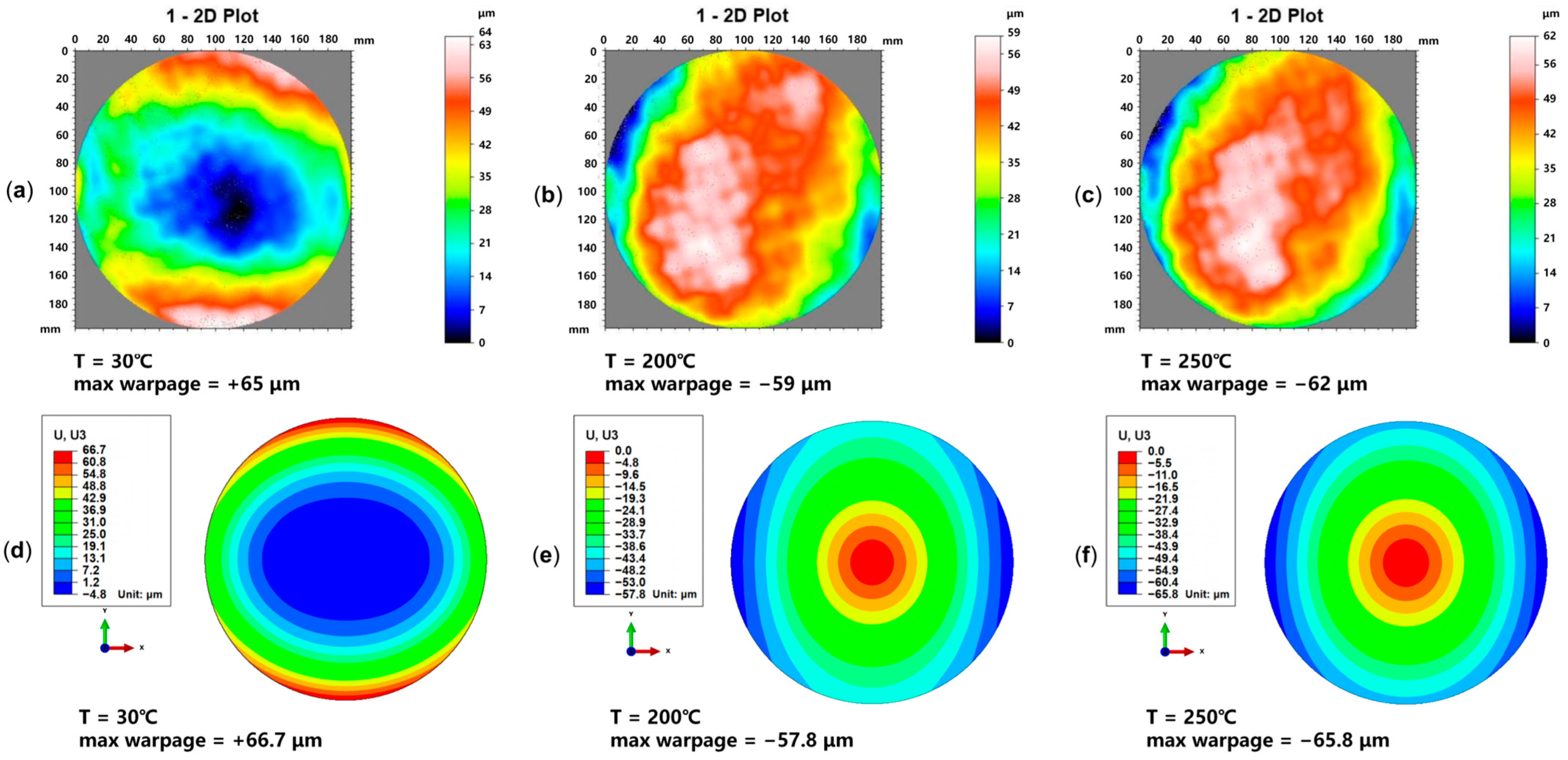
3.1. Validation of Equivalent RDL Wafer Model
3.2. Impact of Increased RDLs on Wafer Warpage
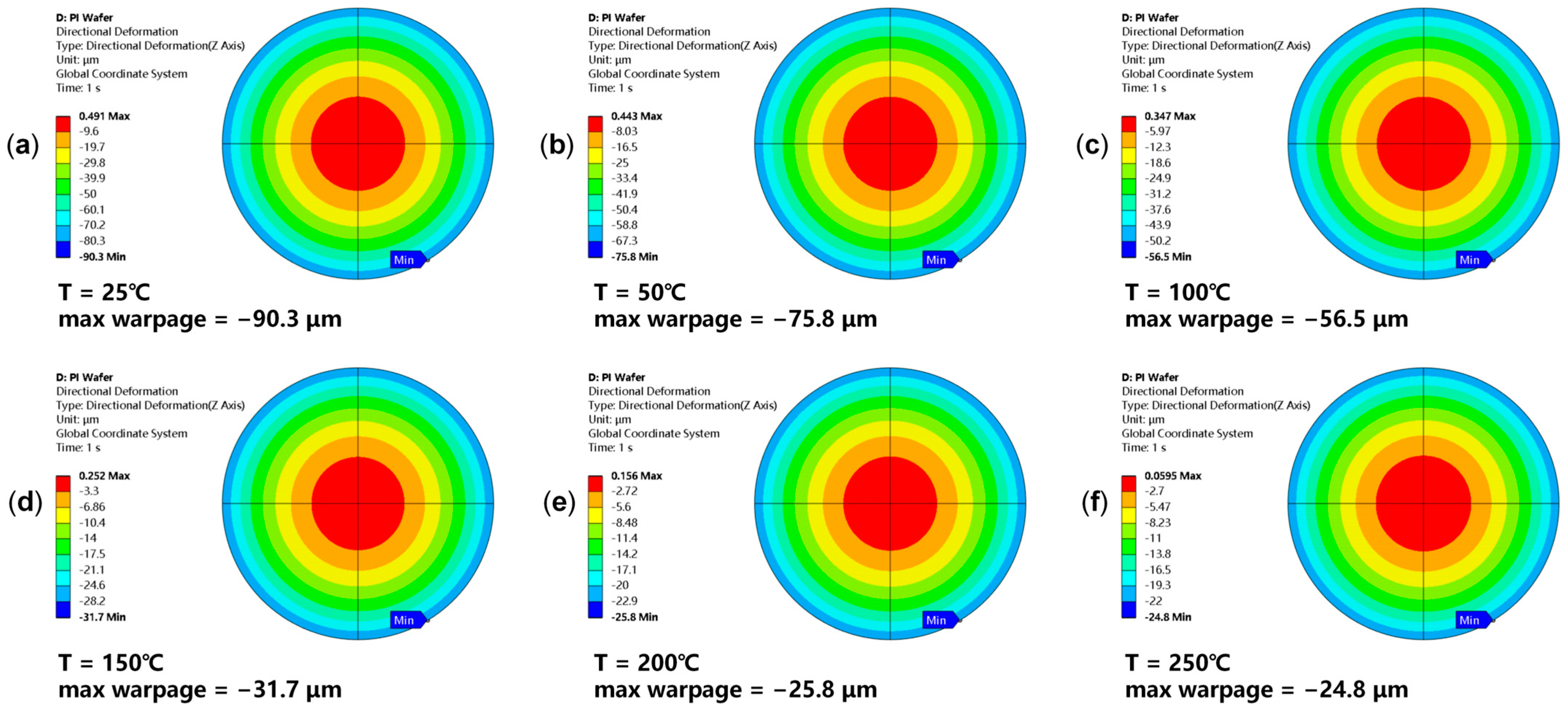
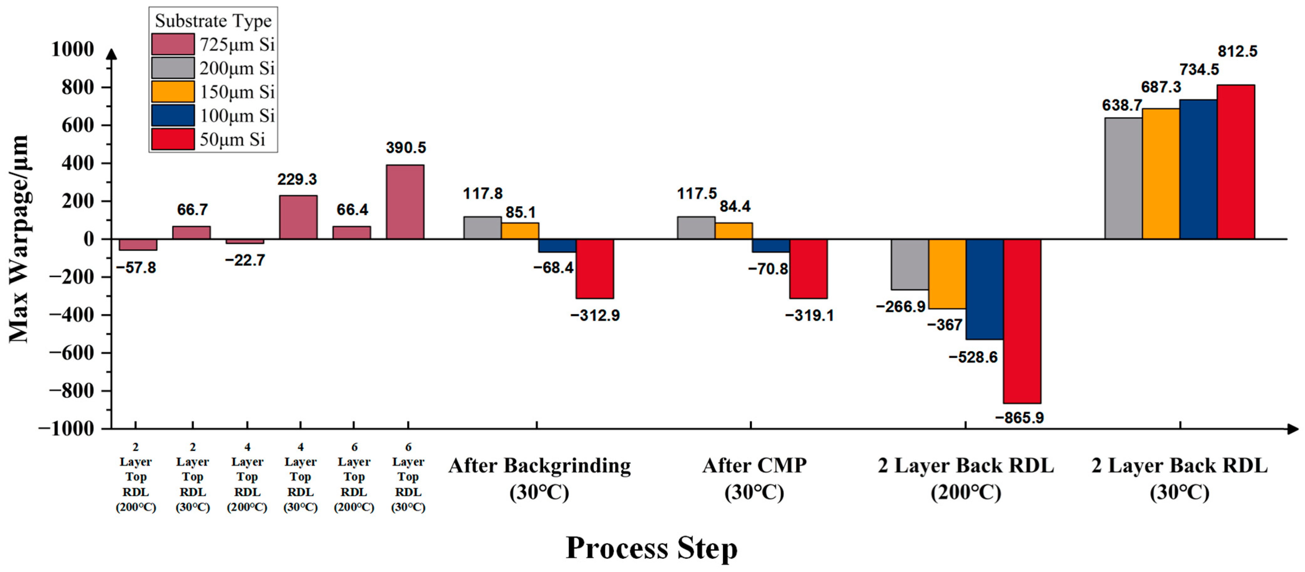
3.3. Warpage Prediction of RDL Wafer at Subsequent Process Steps
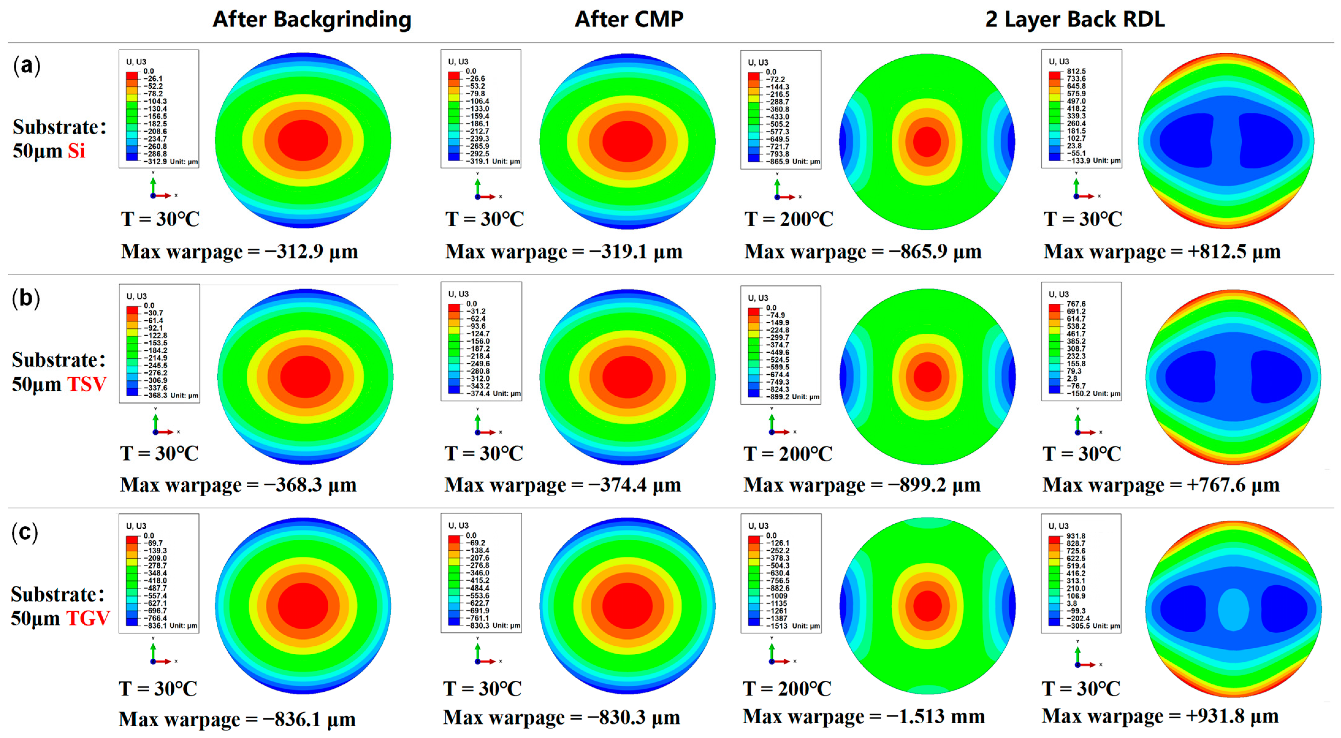
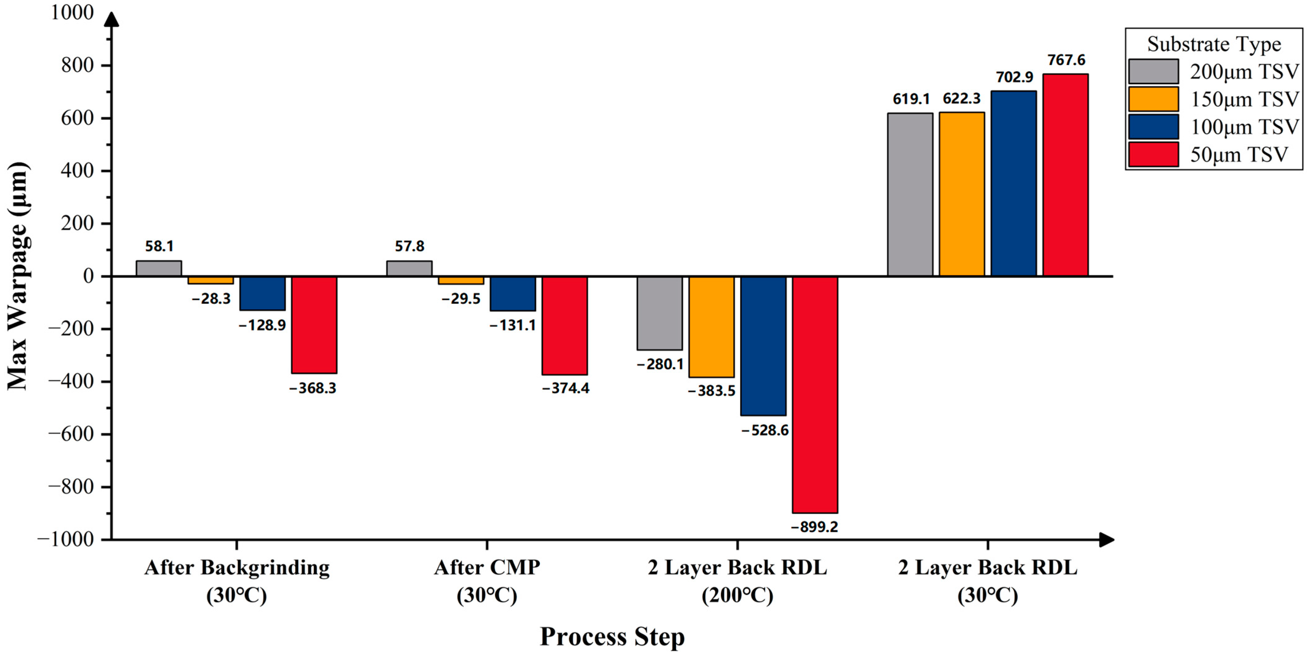
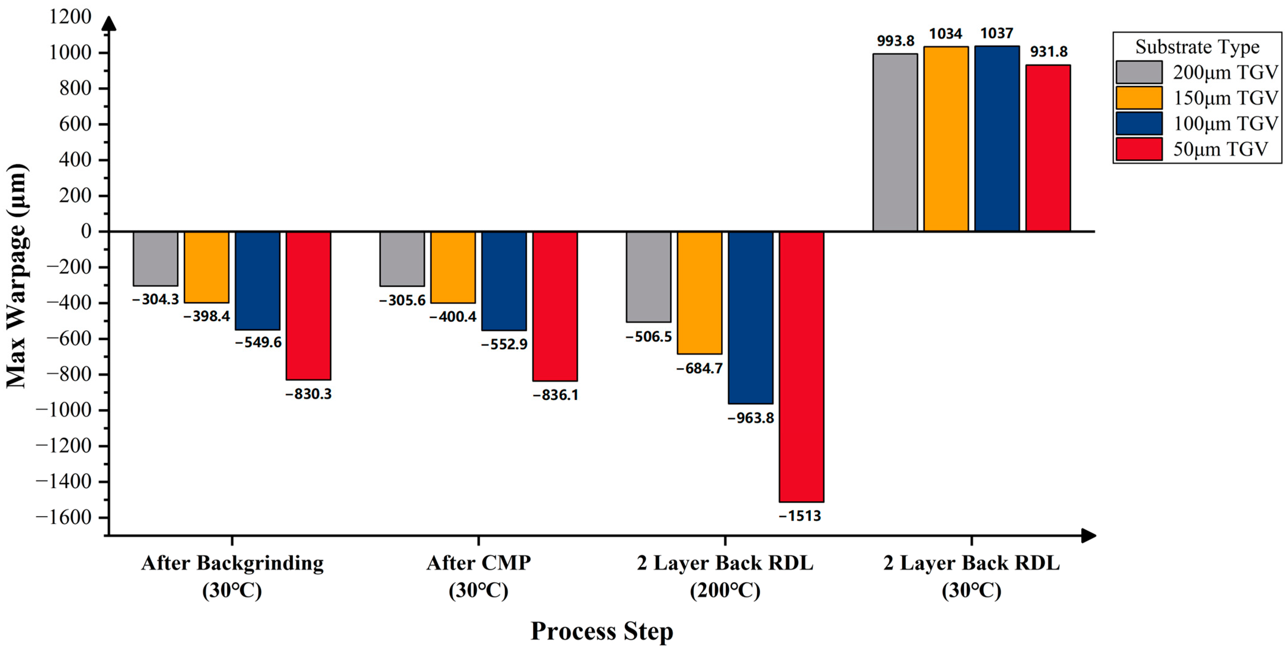
3.4. Impact of Substrate on Wafer Warpage
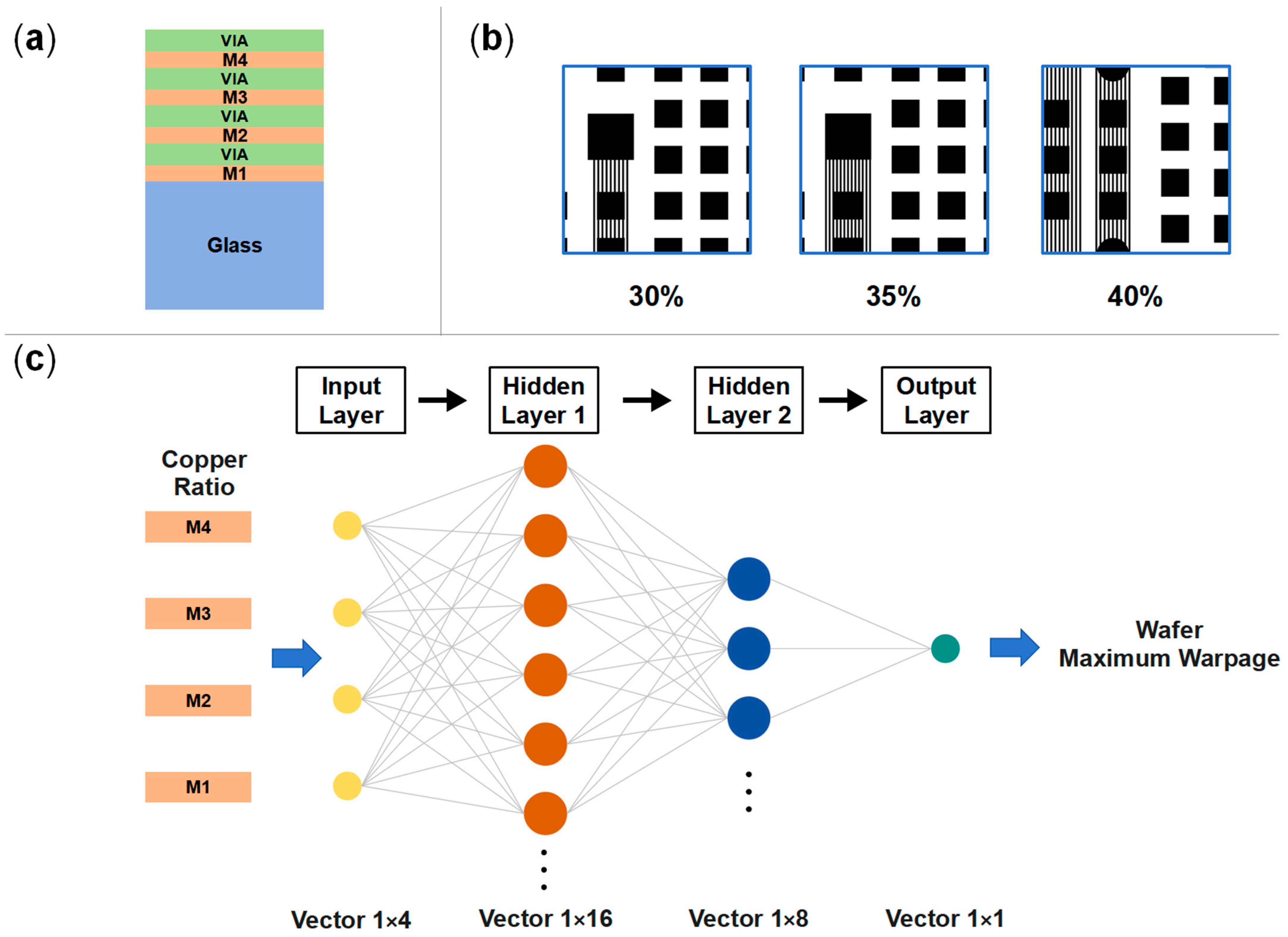
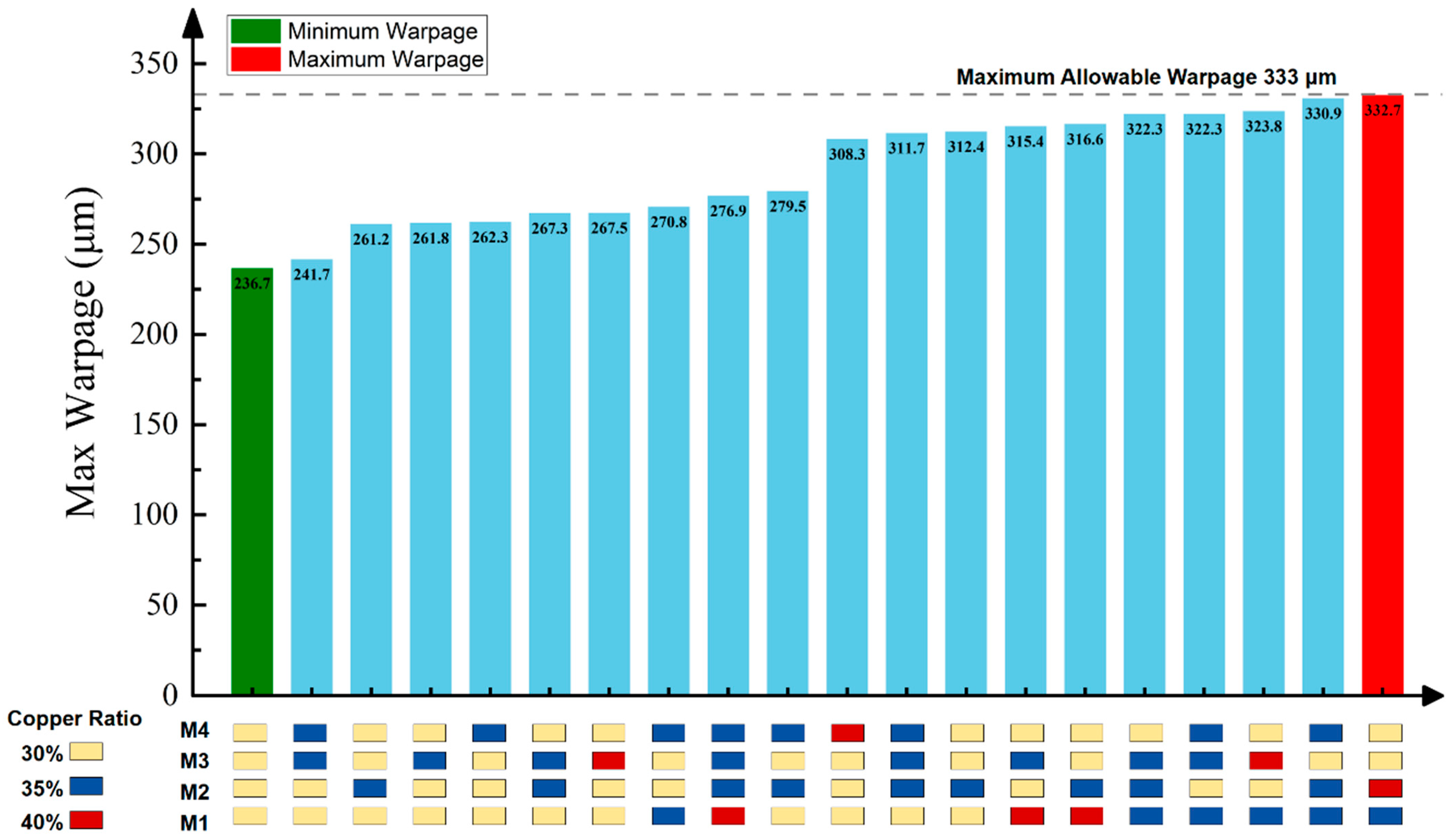
3.5. Neural Network Model for Wafer Warpage Prediction
4. Conclusions
Author Contributions
Funding
Data Availability Statement
Conflicts of Interest
References
- Hu, Y.-C.; Liang, Y.-M.; Hu, H.-P.; Tan, C.-Y.; Shen, C.-T.; Lee, C.-H.; Hou, S.Y. CoWoS Architecture Evolution for Next Generation HPC on 2.5D System in Package. In Proceedings of the 2023 IEEE 73rd Electronic Components and Technology Conference (ECTC), Orlando, FL, USA, 30 May–2 June 2023; pp. 1022–1026. [Google Scholar]
- Ingerly, D.; Amin, S.; Aryasomayajula, L.; Balankutty, A.; Borst, D.; Chandra, A.; Cheemalapati, K.; Cook, C.; Criss, R.; Enamul, K. Foveros: 3D integration and the use of face-to-face chip stacking for logic devices. In Proceedings of the 2019 IEEE International Electron Devices Meeting (IEDM), San Francisco, CA, USA, 7–11 December 2019; pp. 19.16.11–19.16.14. [Google Scholar]
- Scott, G.J.; Bae, J.; Yang, K.; Ki, W.; Whitchurch, N.; Kelly, M.; Zwenger, C.; Jeon, J.; Hwang, T. Heterogeneous Integration Using Organic Interposer Technology. In Proceedings of the 2020 IEEE 70th Electronic Components and Technology Conference (ECTC), Orlando, FL, USA, 3–30 June 2020; pp. 885–892. [Google Scholar]
- Morikawa, Y.; Hironiwa, D.; Murayama, T. Polyimide Fine-via Etching and Low-damage Surface-modification Process For High-density Fan-out Wafer Level Package. In Proceedings of the 2020 IEEE 70th Electronic Components and Technology Conference (ECTC), Orlando, FL, USA, 3–30 June 2020; pp. 900–905. [Google Scholar]
- Choi, J.; Jin, J.; Kang, G.; Hwang, H.; Kim, B.; Yun, H.; Park, J.; Lee, C.; Kang, U.-B.; Lee, J. Novel Approach to Highly Robust Fine Pitch RDL Process. In Proceedings of the 2021 IEEE 71st Electronic Components and Technology Conference (ECTC), Virtual, 1 June–4 July 2021; pp. 2246–2251. [Google Scholar]
- Takano, T.; Kudo, H.; Tanaka, M.; Akazawa, M. Submicron-Scale Cu RDL Pattering Based on Semi-Additive Process for Heterogeneous Integration. In Proceedings of the 2019 IEEE 69th Electronic Components and Technology Conference (ECTC), Las Vegas, NV, USA, 28–31 May 2019; pp. 94–100. [Google Scholar]
- Lau, J.H.; Chen, G.C.-F.; Huang, J.Y.-C.; Chou, R.T.-S.; Yang, C.C.-L.; Liu, H.-N.; Tseng, T.-J. Hybrid Substrate by Fan-Out RDL-First Panel-Level Packaging. IEEE Trans. Compon. Packag. Manuf. Technol. 2021, 11, 1301–1309. [Google Scholar] [CrossRef]
- Netzband, C.; Ryan, K.; Mimura, Y.; Ilseok, S.; Aizawa, H.; Ip, N.; Chen, X.; Fukushima, H.; Tan, S. 0.5 μm Pitch Next Generation Hybrid Bonding with High Alignment Accuracy for 3D Integration. In Proceedings of the 2023 IEEE 73rd Electronic Components and Technology Conference (ECTC), Orlando, FL, USA, 30 May–2 June 2023; pp. 1100–1104. [Google Scholar]
- Wong, J.-H.; Wu, N.; Lai, W.-H.; Chen, D.-L.; Chen, T.-Y.; Chen, C.-H.; Wu, Y.-H.; Chang, Y.-s.; Kao, C.-L.; Tarng, D.; et al. Warpage and RDL Stress Analysis in Large Fan-Out Package with Multi-Chiplet Integration. In Proceedings of the 2022 IEEE 72nd Electronic Components and Technology Conference (ECTC), San Diego, CA, USA, 31 May–3 June 2022; pp. 1074–1079. [Google Scholar]
- Chen, C.; Su, M.; Ma, R.; Zhou, Y.; Li, J.; Cao, L. Investigation of Warpage for Multi-Die Fan-Out Wafer-Level Packaging Process. Materials 2022, 15, 1683. [Google Scholar] [CrossRef] [PubMed]
- Rao, B.S.S.C.; Kumar, M.D.; Sekhar, V.N.; Daniel, I.C.; Tippabhotla, S.K.; Chong, S.C.; C, H.K.; Rao, V.S. Dielectric Stack Optimization for Die-level Warpage Reduction for Chip-to-Wafer Hybrid Bonding. In Proceedings of the 2024 IEEE 74th Electronic Components and Technology Conference (ECTC), Denver, CO, USA, 28–31 May 2024; pp. 62–68. [Google Scholar]
- Xi Ong, E.Y.; Guan, C.G.; Lee, W. Fusion Bonding with Ultra-Thin Dielectric Layers for Photonic Interposer Applications. In Proceedings of the 2024 IEEE 26th Electronics Packaging Technology Conference (EPTC), Singapore, 3–6 December 2024; pp. 131–134. [Google Scholar]
- Nathan, I.; Nejadsadeghi, N.; Kohama, N.; Tanoue, H.; Motoda, K. Distortion Simulation for Direct Wafer-to-Wafer Bonding Process. In Proceedings of the 2023 IEEE 73rd Electronic Components and Technology Conference (ECTC), Orlando, FL, USA, 30 May–2 June 2023; pp. 694–698. [Google Scholar]
- Iacovo, S.; D’Havé, K.; Okudur, O.O.; De Vos, J.; Uhrmann, T.; Plach, T.; Conard, T.; Meersschaut, J.; Bex, P.; Brems, S.; et al. A Study of SiCN Wafer-to-Wafer Bonding and Impact of Wafer Warpage. In Proceedings of the 2023 IEEE 73rd Electronic Components and Technology Conference (ECTC), Orlando, FL, USA, 30 May–2 June 2023; pp. 1410–1417. [Google Scholar]
- Ogawa, T.; Saito, W.; Nishizawa, S.-I. Slit Field Plate Power MOSFET for Improvement of Figure-Of-Merits. IEEE J. Electron Devices Soc. 2021, 9, 552–556. [Google Scholar] [CrossRef]
- Yeap, K.H.; Nisar, H.; Dakulagi, V. Warpage Reduction for Power MOSFET Wafers. Electrica 2021, 21, 173–179. [Google Scholar] [CrossRef]
- Salahouelhadj, A.; Gonzalez, M.; Vanstreels, K.; Van der Plas, G.; Beyer, G.; Beyne, E. Analysis of warpage of a flip-chip BGA package under thermal loading: Finite element modelling and experimental validation. Microelectron. Eng. 2023, 271–272, 111947. [Google Scholar] [CrossRef]
- Feng, W.; Shimamoto, H.; Kawagoe, T.; Honma, I.; Yamasaki, M.; Okutsu, F.; Masuda, T.; Kikuchi, K. Wafer-to-Wafer Bonding Fabrication Process-Induced Wafer Warpage. IEEE Trans. Semicond. Manuf. 2023, 36, 398–403. [Google Scholar] [CrossRef]
- Ji, L.; Chai, T.C.; Siang Lim, S.P. Wafer Warpage Optimization Via Finite Element Analysis for a 3D Chiplet Package. In Proceedings of the 2022 IEEE 24th Electronics Packaging Technology Conference (EPTC), Singapore, 7–9 December 2022; pp. 707–711. [Google Scholar]
- Lee, C.-C.; Wang, C.-W.; Chen, C.-Y. Comparison of Mechanical Modeling to Warpage Estimation of RDL-First Fan-Out Panel-Level Packaging. IEEE Trans. Compon. Packag. Manuf. Technol. 2022, 12, 1100–1108. [Google Scholar] [CrossRef]
- Chen, G.C.-F.; Lau, J.H.; Yang, C.C.-L.; Huang, J.Y.-C.; Peng, A.Y.-J.; Liu, H.-N.; Tseng, T.-J.; Li, M. 2.3D Hybrid Substrate with Ajinomoto Build-Up Film for Heterogeneous Integration. In Proceedings of the 2022 IEEE 72nd Electronic Components and Technology Conference (ECTC), San Diego, CA, USA, 31 May–3 June 2022; pp. 30–37. [Google Scholar]
- Wu, X.; Wang, Z.; Ma, S.; Chu, X.; Li, C.; Wang, W.; Jin, Y.; Wu, D. An RDL Modeling and Thermo-Mechanical Simulation Method of 2.5D/3D Advanced Package Considering the Layout Impact Based on Machine Learning. Micromachines 2023, 14, 1531. [Google Scholar] [CrossRef] [PubMed]
- Wu, M.-L.; Wu, J.-Y. Advanced FOPoP technology in heterogeneous integration: Finite element analysis with element birth and death technique. Simul. Model. Pract. Theory 2025, 138, 103041. [Google Scholar] [CrossRef]
- Pan, L.; Xie, Y.; Yang, H.; Bao, X.; Chen, J.; Zou, M.; Li, R.W. Omnidirectionally Stretchable Spin-Valve Sensor Array with Stable Giant Magnetoresistance Performance. ACS Nano 2025, 19, 5699–5708. [Google Scholar] [CrossRef] [PubMed]
- Ji, L.; Che, F.; Ji, H.; Li, H.; Kawano, M. Modelling and characterization on wafer to wafer hybrid bonding technology for 3D IC packaging. In Proceedings of the 2019 IEEE 21st Electronics Packaging Technology Conference (EPTC), Singapore, 4–6 December 2019; pp. 87–94. [Google Scholar]
- Material: Copper—PVD or Electroplated. Available online: https://www.mit.edu/~6.777/matprops/copper.htm (accessed on 25 March 2025).
- Lau, J.H.; Li, M.; Tian, D.; Fan, N.; Kuah, E.; Kai, W.; Li, M.; Hao, J.; Cheung, Y.M.; Li, Z.; et al. Warpage and Thermal Characterization of Fan-Out Wafer-Level Packaging. IEEE Trans. Compon. Packag. Manuf. Technol. 2017, 7, 1729–1738. [Google Scholar] [CrossRef]
- Wu, X.; Li, C.; Ma, S. TSV wafer warpage simulation and process induced strain prediction by machine learning-based anisotropic equivalent modeling method. In Proceedings of the 2023 IEEE 25th Electronics Packaging Technology Conference (EPTC), Singapore, 5–8 December 2023; pp. 780–786. [Google Scholar]
- Xu, Q.; Fang, D.; Zhang, X.; Chen, Y.; Wang, X.; Cai, Y.; Zhang, B.; Wei, Z. Etch the borosilicate glass to form a straight through-glass-via based on the FLACE technology. J. Micromech. Microeng. 2022, 32, 055008. [Google Scholar] [CrossRef]


| Materials | Young’s Modulus (GPa) | Poisson’s Ratio | Thermal Expansion Coefficient (ppm/°C) | Thermal Conductivity (W/m·K) | Density (kg/m3) |
|---|---|---|---|---|---|
| Si [25] | 131 | 0.28 | 2.6 | 145.87 | 2.329 |
| SiO2 [18] | 73 | 0.17 | 0.55 | 1.1 | 2.300 |
| Cu [26] | 130 | 0.34 | 16.4 | 401 | 8.960 |
| PI | 2.5 | 0.35 | 54 (25 °C) 50 (50 °C) 47 (100 °C) 35 (150 °C) 44.5 (200 °C) 122 (250 °C) | 0.12 | 1.420 |
| Glass | 64 | 0.20 | 3.25 | 1.2 | 2.230 |
| Materials | Young’s Modulus (GPa) | Poisson’s Ratio | Shear Modulus (GPa) | CTE (ppm/°C) | Thermal Conductivity (W/m·K) | Density (kg/m3) |
|---|---|---|---|---|---|---|
| Equivalent TSV (h = 50 μm) | Ex = 130.997868 | νxy = 0.280822 | Gxy = 51.138030 | αx = 2.789632 | Kx = 147.549900 | 2.410 |
| Ey = 130.997868 | νxz = 0.281142 | Gxz = 51.138315 | αy = 2.789632 | Ky = 147.549900 | ||
| Ez = 130.994392 | νyz = 0.281146 | Gyz = 51.138314 | αz = 2.873377 | Kz = 149.000899 | ||
| Equivalent TSV (h = 100 μm) | Ex = 130.998558 | νxy = 0.280829 | Gxy = 51.138030 | αx = 2.791227 | Kx = 147.549900 | 2.410 |
| Ey = 130.998558 | νxz = 0.280973 | Gxz = 51.138315 | αy = 2.791227 | Ky = 147.549900 | ||
| Ez = 130.994393 | νyz = 0.280975 | Gyz = 51.138315 | αz = 2.828727 | Kz = 149.000899 | ||
| Equivalent TSV (h = 150 μm) | Ex = 130.998788 | νxy = 0.280831 | Gxy = 51.138030 | αx = 2.791696 | Kx = 147.549899 | 2.410 |
| Ey = 130.998788 | νxz = 0.280931 | Gxz = 51.138315 | αy = 2.791696 | Ky = 147.549899 | ||
| Ez = 130.994393 | νyz = 0.280930 | Gyz = 51.138315 | αz = 2.817442 | Kz = 149.000899 | ||
| Equivalent TSV (h = 200 μm) | Ex = 130.998903 | νxy = 0.280832 | Gxy = 51.138030 | αx = 2.791925 | Kx = 147.549899 | 2.410 |
| Ey = 130.998903 | νxz = 0.280899 | Gxz = 51.138315 | αy = 2.791925 | Ky = 147.549899 | ||
| Ez = 130.994392 | νyz = 0.280898 | Gyz = 51.138315 | αz = 2.809058 | Kz = 149.000899 |
| Materials | Young’s Modulus (GPa) | Poisson’s Ratio | Shear Modulus (GPa) | CTE (ppm/°C) | Thermal Conductivity (W/m·K) | Density (kg/m3) |
|---|---|---|---|---|---|---|
| Equivalent TGV (h = 50 μm) | Ex = 64.494801 | νxy = 0.201541 | Gxy = 26.838356 | αx = 3.467406 | Kx = 1.229639 | 2.312 |
| Ey = 64.494801 | νxz = 0.201408 | Gxz = 26.857501 | αy = 3.467406 | Ky = 1.229639 | ||
| Ez = 64.831363 | νyz = 0.201373 | Gyz = 26.857501 | αz = 3.703234 | Kz = 6.106258 | ||
| Equivalent TGV (h = 100 μm) | Ex = 64.494989 | νxy = 0.201543 | Gxy = 26.838356 | αx = 3.468674 | Kx = 1.229639 | 2.312 |
| Ey = 64.494989 | νxz = 0.201344 | Gxz = 26.857501 | αy = 3.468674 | Ky = 1.229639 | ||
| Ez = 64.831363 | νyz = 0.201327 | Gyz = 26.857502 | αz = 3.659611 | Kz = 6.106258 | ||
| Equivalent TGV (h = 150 μm) | Ex = 64.495051 | νxy = 0.201544 | Gxy = 26.838356 | αx = 3.469015 | Kx = 1.229639 | 2.312 |
| Ey = 64.495051 | νxz = 0.201319 | Gxz = 26.857501 | αy = 3.469015 | Ky = 1.229639 | ||
| Ez = 64.831363 | νyz = 0.201328 | Gyz = 26.857502 | αz = 3.650259 | Kz = 6.106258 | ||
| Equivalent TGV (h = 200 μm) | Ex = 64.495082 | νxy = 0.201544 | Gxy = 26.838356 | αx = 3.469169 | Kx = 1.229639 | 2.312 |
| Ey = 64.495082 | νxz = 0.201308 | Gxz = 26.857501 | αy = 3.469169 | Ky = 1.229639 | ||
| Ez = 64.831363 | νyz = 0.201317 | Gyz = 26.857502 | αz = 3.641562 | Kz = 6.106258 |
Disclaimer/Publisher’s Note: The statements, opinions and data contained in all publications are solely those of the individual author(s) and contributor(s) and not of MDPI and/or the editor(s). MDPI and/or the editor(s) disclaim responsibility for any injury to people or property resulting from any ideas, methods, instructions or products referred to in the content. |
© 2025 by the authors. Licensee MDPI, Basel, Switzerland. This article is an open access article distributed under the terms and conditions of the Creative Commons Attribution (CC BY) license (https://creativecommons.org/licenses/by/4.0/).
Share and Cite
Chu, X.; Wang, S.; Li, C.; Wang, Z.; Ma, S.; Wu, D.; Yuan, H.; You, B. Modeling and Simulation for Predicting Thermo-Mechanical Behavior of Wafer-Level Cu-PI RDLs During Manufacturing. Micromachines 2025, 16, 582. https://doi.org/10.3390/mi16050582
Chu X, Wang S, Li C, Wang Z, Ma S, Wu D, Yuan H, You B. Modeling and Simulation for Predicting Thermo-Mechanical Behavior of Wafer-Level Cu-PI RDLs During Manufacturing. Micromachines. 2025; 16(5):582. https://doi.org/10.3390/mi16050582
Chicago/Turabian StyleChu, Xianglong, Shitao Wang, Chunlei Li, Zhizhen Wang, Shenglin Ma, Daowei Wu, Hai Yuan, and Bin You. 2025. "Modeling and Simulation for Predicting Thermo-Mechanical Behavior of Wafer-Level Cu-PI RDLs During Manufacturing" Micromachines 16, no. 5: 582. https://doi.org/10.3390/mi16050582
APA StyleChu, X., Wang, S., Li, C., Wang, Z., Ma, S., Wu, D., Yuan, H., & You, B. (2025). Modeling and Simulation for Predicting Thermo-Mechanical Behavior of Wafer-Level Cu-PI RDLs During Manufacturing. Micromachines, 16(5), 582. https://doi.org/10.3390/mi16050582