


Design and Fabrication of Silicon Pressure Sensors Based on Wet Etching Technology

 , and
, and 
Abstract
1. Introduction
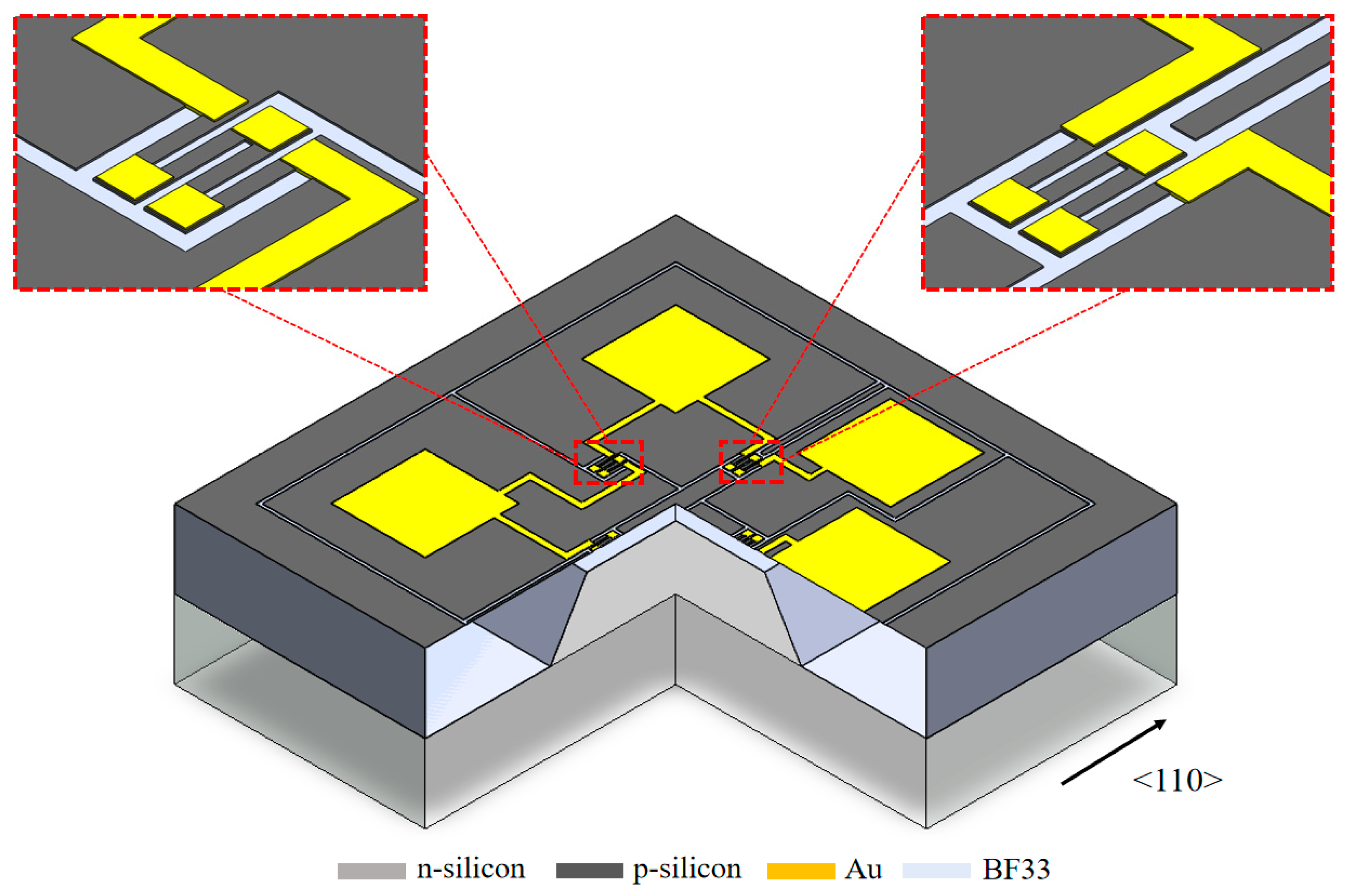
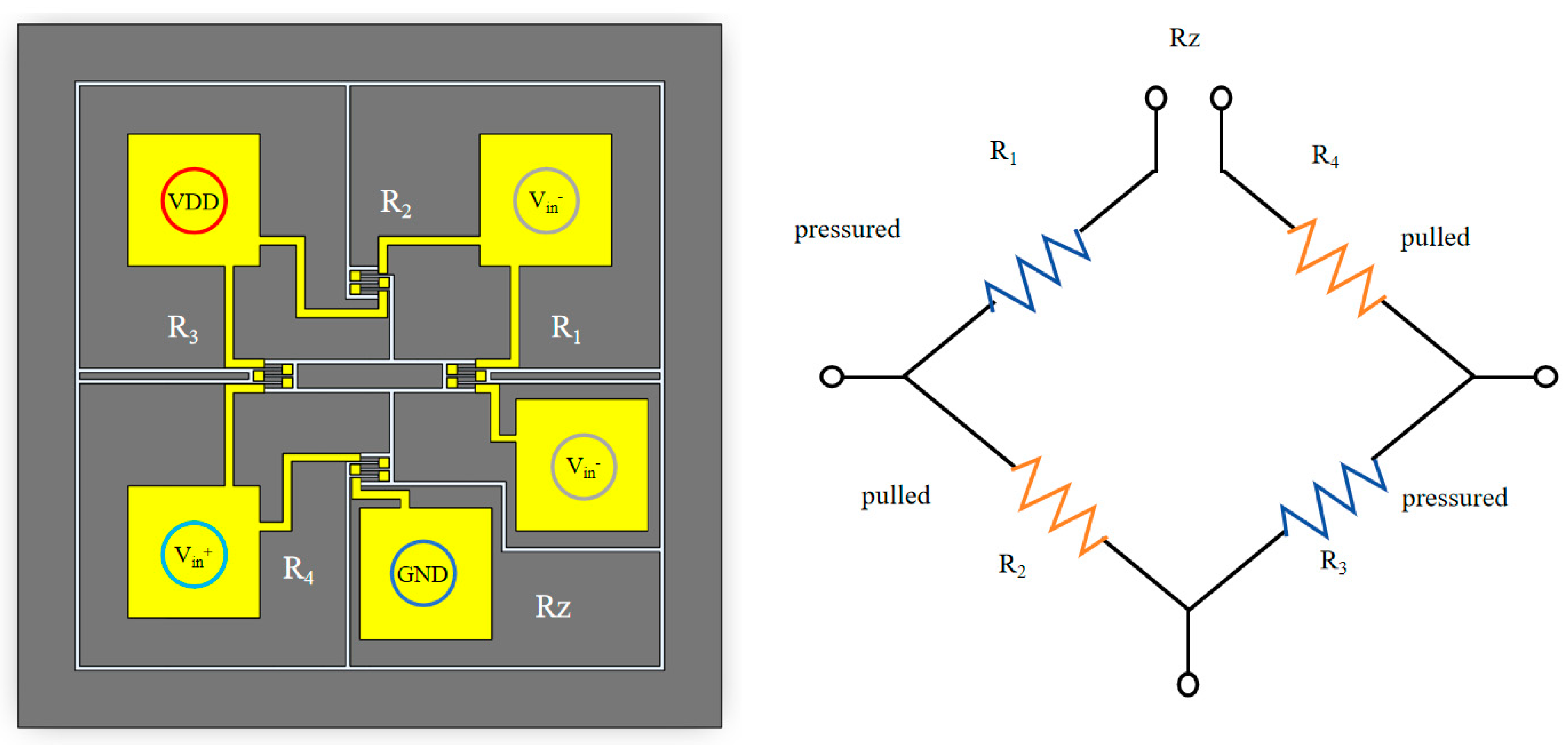
2. Theory, Design, and Simulation
3. Fabrication
3.1. Material and Characterization
3.1.1. Etching Rate and Roughness Analysis
3.1.2. Effect of Sensitive Membrane Roughness on Sensor Performance
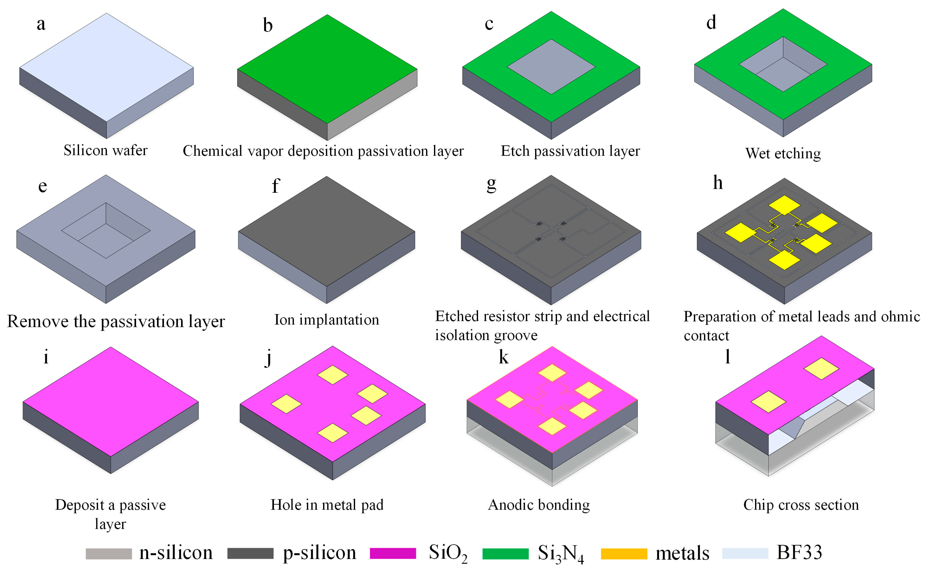
3.2. Manufacture of Pressure Sensors
- A 4-inch double-sided polished silicon wafer (100) with a thickness of 500 μm and a resistivity of 1–10 Ω cm is prepared.
- A thin layer of dioxide (300 nm) and a thin layer of nitride (300 nm), which are attached to both sides of the silicon wafer, are grown on the wafer by low-pressure chemical vapor deposition (LPCVD). The passivation layer is mainly used as a mask in the wet etching process.
- The oxide and nitride layers are dry etched by reactive ion etching (RIE), windowing the subsequent areas that require wet etching, and areas that do not require wet etching are still protected by the passivation layer.
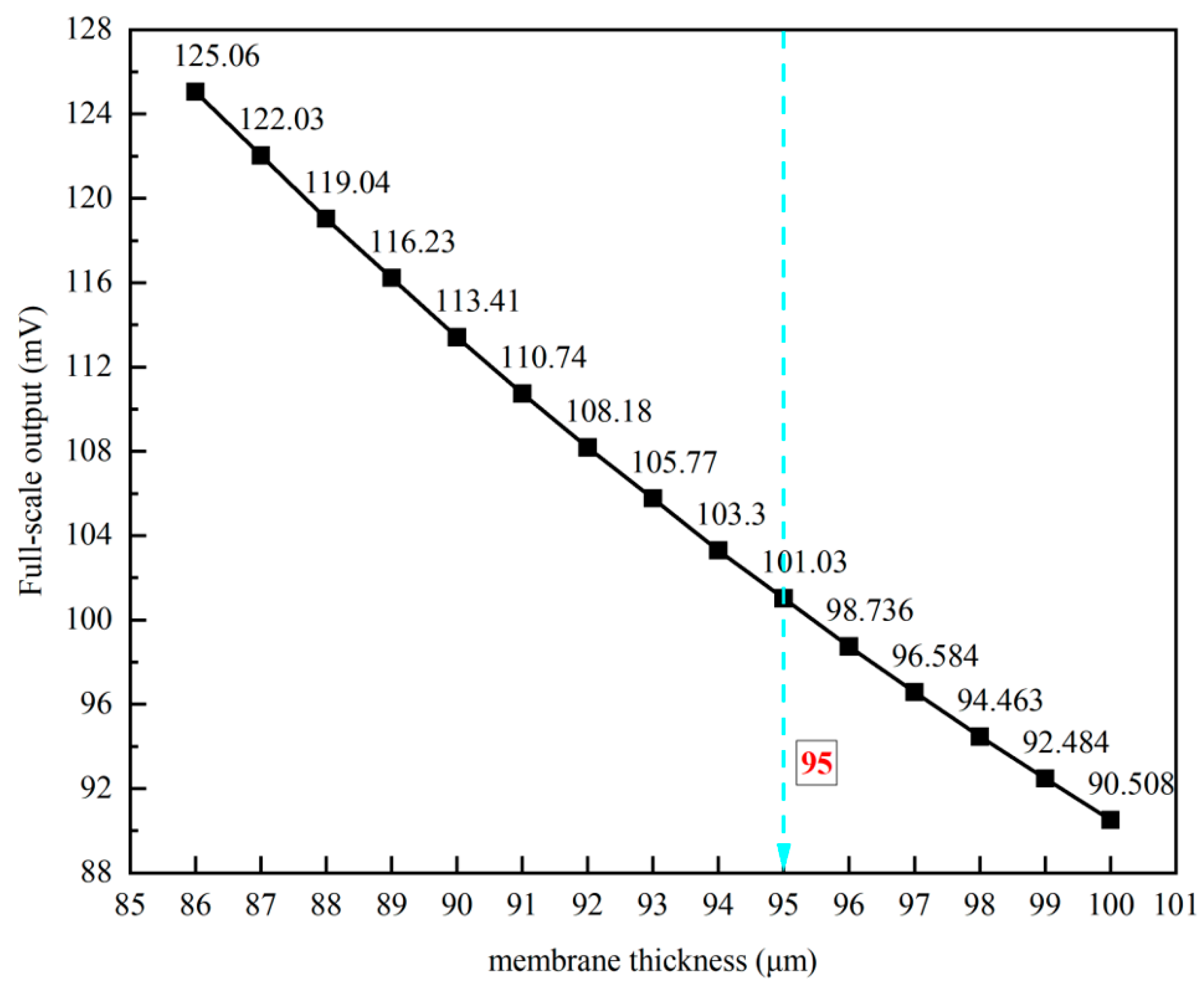
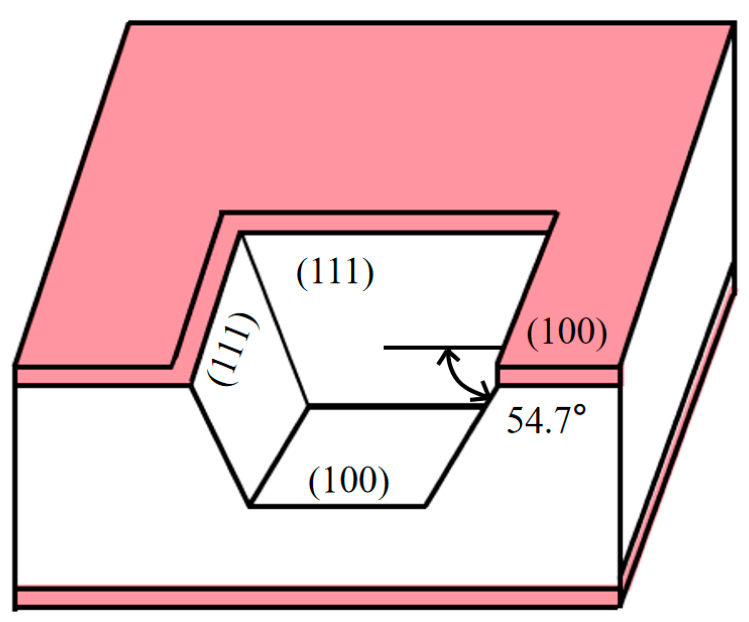
- Taking advantage of the high selectivity of silicon for wet etching in alkaline solutions, it was etched in a 25% tetramethylammonium hydroxide (TMAH) solution for about 17 h, and the etching was stopped when the thickness of the sensitive film reached 95 μm.
- The silicon nitride layer on both sides of the wafer is precisely removed using a reactive ion etching process, followed by the removal of the silicon oxide layer on both sides of the wafer using a BOE solution at a constant temperature of 40 °C [25] in a water bath to ensure that all passivation layers are completely removed.
- Ion injection of boron into the device layer is performed to complete the doping of the entire surface of the device layer. After ion implantation, the device was annealed for 20 min at 1000 °C to repair lattice damage.
- The deep silicon etching technique is utilized to pattern the device layers and prepare the piezoresistors and electrical isolation tanks.
- To form good ohmic contact, besides heavily doping the semiconductor surface, it also requires that the metals have a matching work function. For this reason, we chose metal Au material to prepare metal thin films by magnetron sputtering and to make leads and pads by peeling (Ti 50 nm, Pt 50 nm, Au 500 nm).
- A thin oxide layer is deposited on top of the prepared device layer using low-pressure chemical vapor deposition to protect the device layer from oxidation and significantly improve the stability and reliability of the device.
- Dry etching of the oxide layer by reactive ion etching exposes the sputtered metal pads in h to provide a reliable connection interface for gold lead bonding in the subsequent packaging process.
- Absolute pressure reference chamber by anodic bonding of silicon and glass (temperature 400 °C, pressure 1250 N, voltage 800 V) is performed.
- Cross-section of the overall MEMS chip structure is performed.
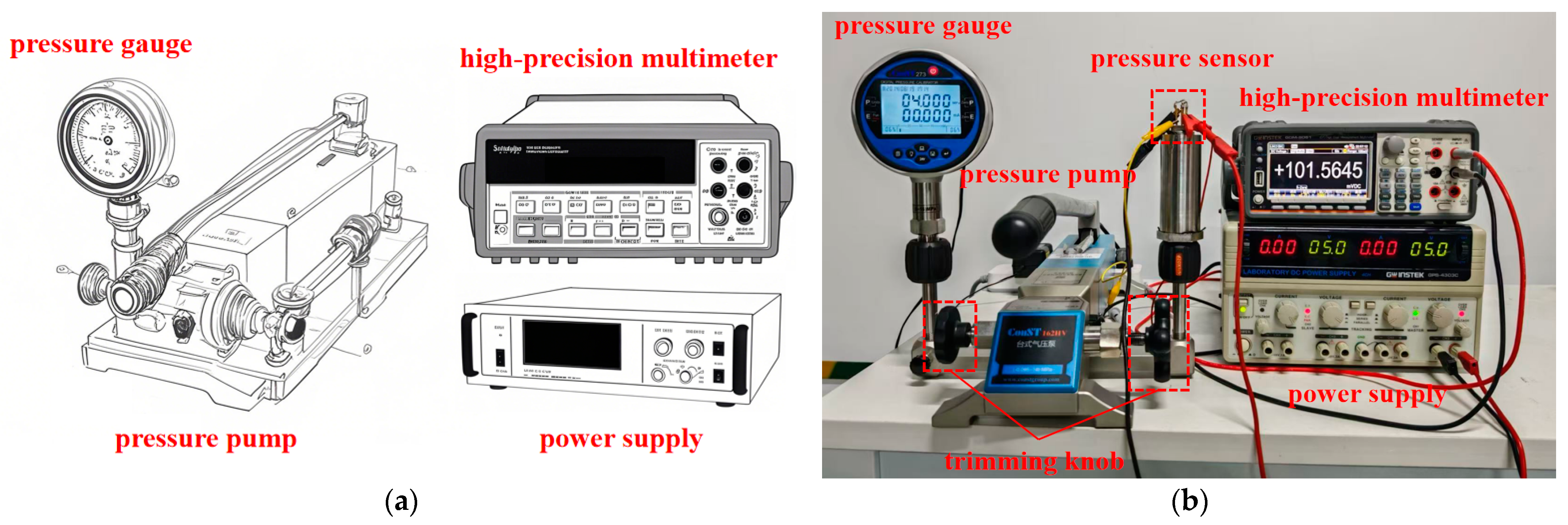
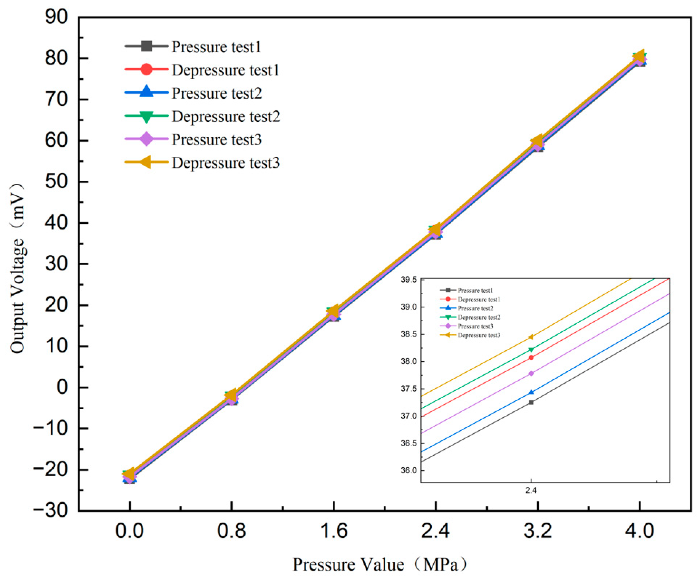
4. Measurement and Discussion
5. Conclusions
Author Contributions
Funding
Data Availability Statement
Conflicts of Interest
References
- San, H.; Zhang, H.; Zhang, Q.; Yu, Y.; Chen, X. Silicon–glass-based single piezoresistive pressure sensors for harsh environment applica-tions. J. Micromech. Microeng. 2013, 23, 75020. [Google Scholar] [CrossRef]
- Zheng, B.R.; Zhou, C.; Wang, Q.; Pan, X.M.; Xue, W. Ultra-small micro pressure sensor chip design and fabrication featuring high-sensitivity and good-linearity. Microsyst. Technol. 2014, 21, 173–179. [Google Scholar] [CrossRef]
- Pham, A.-D.; Nguyen, T.K.; Le, H.H.; Dang, P.V. An Efficient Design of the Piezoresistive Pressure Sensor Applied for Micro Aerial Vehicle. Int. J. Integr. Eng. 2023, 15, 35–44. [Google Scholar] [CrossRef]
- Zhou, M.; Zhou, S.; Zhou, Z.; Jiang, S.; Zhang, W. Design, fabrication, and thermal zero drift compensation of a SOI pressure sensor for high temperature applications. Sens. Actuators A Phys. 2024, 382. [Google Scholar] [CrossRef]
- Ma, Y.; Lei, C.; Liang, T.; Jia, P.; Li, Z.; Wang, W.; Xiong, J.; Wang, B.; Chen, G. Design and fabrication of a tiny micro-pressure sensor with improved linearity and sensitivity. Phys. Scr. 2023, 98, 055018. [Google Scholar] [CrossRef]
- Pinto, R.M.; Gund, V.; Calaza, C.; Nagaraja, K.; Vinayakumar, K. Piezoelectric aluminum nitride thin-films: A review of wet and dry etching techniques. Microelectron. Eng. 2022, 257. [Google Scholar] [CrossRef]
- Mondal, S.; Kalaga, P.S.; Krishnan, P.S.R.; Shenp, A.D. Study on the kinetics of standalone Si micro-pyramid formation using tetra methyl ammonium hydroxide as etchant. Mater. Sci. Semicond. Process. 2023, 158, 107341. [Google Scholar] [CrossRef]
- Aprilia, L.; Meguro, T.; Tabei, T.; Mimura, H.; Kuroki, S.-I. Controlled Release of Microcantilever from a Silicon-on-Insulator Wafer with Oxide Brace. In Proceedings of the 2021 International Conference on Radar, Antenna, Microwave, Electronics, and Telecommunications (ICRAMET), Bandung, Indonesia, 23–24 November 2021; pp. 219–222. [Google Scholar]
- Shen, J.; Chen, Y.; Zhang, F.; Zhang, D.; Gan, Y. Morphological and crystallographic evolution of patterned silicon substrate etched in TMAH solutions. Appl. Surf. Sci. 2019, 496, 143720. [Google Scholar] [CrossRef]
- Shao, Z.; Wu, Y.; Wang, S.; Zhang, C.Z.; Sun, Z.; Yan, M.; Shang, Y.; Song, E.; Liu, Z. All-sapphire-based fiber-optic pressure sensor for high-temperature applications based on wet etching. Opt. Express 2021, 29, 4139–4146. [Google Scholar] [CrossRef]
- Jun, K.-H.; Kim, B.-J.; Kim, J.-S. Effect of additives on the anisotropic etching of silicon by using a TMAH based solution. Electron. Mater. Lett. 2015, 11, 871–880. [Google Scholar] [CrossRef]
- Gupta, A.; Pal, P.; Sharma, C.S. Surface Texturing of Silicon {100} in an Extremely Low Concentration TMAH for Minimized Reflectivity. ECS J. Solid State Sci. Technol. 2019, 8, P622–P628. [Google Scholar] [CrossRef]
- Choi, J.-H.; Kim, J.-S. Design and fabrication of ultrathin silicon-based strain gauges for piezoresistive pressure sensor. Curr. Appl. Phys. 2025, 69, 28–35. [Google Scholar] [CrossRef]
- Hu, N. Coherence of wall pressure fluctuations in zero and adverse pressure gradients. J. Sound Vib. 2021, 511, 116316. [Google Scholar] [CrossRef]
- Tang, X.; Tian, J.; Zhao, J.; Jin, Z.; Liu, Y.; Liu, J.; Chen, T.; Li, J. Structure design and optimization of SOI high-temperature pressure sensor chip. Microelectron. J. 2021, 118, 105245. [Google Scholar] [CrossRef]
- Paliwal, S.; Yenuganti, S. Design and Simulation of Digital Output MEMS Pressure Sensor. Arab. J. Sci. Eng. 2020, 45, 6661–6673. [Google Scholar] [CrossRef]
- Guan, T.; Yang, F.; Wang, W.; Huang, X.; Jiang, B.; Zhang, D. The Design and Analysis of Piezoresistive Shuriken-Structured Diaphragm Micro-Pressure Sensors. J. Microelectromech. Syst. 2016, 26, 206–214. [Google Scholar] [CrossRef]
- Purohit, S.; Swarnalatha, V.; Pandey, A.K.; Pal, P. Wet anisotropic etching characteristics of Si{111} in NaOH-based solution for silicon bulk micromachining. Micro Nano Syst. Lett. 2022, 10, 21. [Google Scholar] [CrossRef]
- Fan, X.; Wang, L.; Zhang, S. A High-Performance Micro Differential Pressure Sensor. Micromachines 2024, 15, 1396. [Google Scholar] [CrossRef]
- Yusoh, S.N.; Yaacob, K.A. Effect of tetramethylammonium hydroxide/isopropyl alcohol wet etching on geometry and surface roughness of silicon nanowires fabricated by AFM lithography. Beilstein J. Nanotechnol. 2016, 7, 1461–1470. [Google Scholar] [CrossRef]
- Ma, T.; Wang, Y.; Zhou, J. A Si-based suspended tunnel structure with trapezoidal section by two-step etching. J. Micromech. Microeng. 2022, 32, 24003. [Google Scholar] [CrossRef]
- Mrazkova, Z.; Sobkowicz, I.P.; Foldyna, M.; Postava, K.; Florea, I.; Pištora, J.; Roca i Cabarrocas, P. Optical properties and performance of pyramidal texture silicon heterojunction solar cells: Key role of vertex angles. Prog. Photovolt. Res. Appl. 2018, 26, 369–376. [Google Scholar] [CrossRef]
- Pal, P.; Swarnalatha, V.; Rao, A.V.N.; Pandey, A.K.; Tanaka, H.; Sato, K. High speed silicon wet anisotropic etching for applications in bulk micromachining: A review. Micro Nano Syst. Lett. 2021, 9, 1–59. [Google Scholar] [CrossRef]
- Smiljanić, M.M.; Lazić, Ž.; Radjenović, B.; Radmilović-Radjenović, M.; Jović, V. Evolution of Si Crystallographic Planes-Etching of Square and Circle Patterns in 25 wt % TMAH. Micromachines 2019, 10, 102. [Google Scholar] [CrossRef] [PubMed]
- Aprilia, L.; Meguro, T.; Nuryadi, R.; Tabei, T.; Mimura, H.; Kuroki, S.-I. Integrated Fabrication Process of Si Microcantilever Using TMAH Solution with Planar Molybdenum Mask. J. Microelectromech. Syst. 2023, 32, 290–296. [Google Scholar] [CrossRef]
- Swarnalatha, V.; Narasimha Rao, A.V.; Ashok, A.; Singh, S.S.; Pal, P. Modified TMAH based etchant for improved etching characteristics on Si{1 0 0} wafer. J. Micromech. Microeng. 2017, 27, 85003. [Google Scholar] [CrossRef]
- Pal, P.; Sato, K.; A Gosalvez, M.; Tang, B.; Hida, H.; Shikida, M. Fabrication of novel microstructures based on orientation-dependent adsorption of surfactant molecules in a TMAH solution. J. Micromech. Microeng. 2010, 21, 15008. [Google Scholar] [CrossRef]
- Pal, P.; Sato, K. Fabrication methods based on wet etching process for the realization of silicon MEMS structures with new shapes. Microsyst. Technol. 2010, 16, 1165–1174. [Google Scholar] [CrossRef]
- Zubel, I.; Kramkowska, M.; Rola, K. Silicon anisotropic etching in TMAH solutions containing alcohol and surfactant addi-tives. Sens. Actuators A Phys. 2012, 178, 126–135. [Google Scholar] [CrossRef]
- Li, C.; Jia, P.; Sun, B.; Hong, Y.; Xue, Y.; Jia, M.; Xiong, J. A Differential Split-Type Pressure Sensor for High-Temperature Applications. IEEE Access 2021, 9, 20641–20647. [Google Scholar] [CrossRef]
- Li, C.; Sun, B.; Jia, P.; Xue, Y.; Jia, M.; Xiong, J. Capacitive Pressure Sensor with Integrated Signal-Conversion Circuit for High-Temperature Applications. IEEE Access 2020, 8, 212787–212793. [Google Scholar] [CrossRef]


Disclaimer/Publisher’s Note: The statements, opinions and data contained in all publications are solely those of the individual author(s) and contributor(s) and not of MDPI and/or the editor(s). MDPI and/or the editor(s) disclaim responsibility for any injury to people or property resulting from any ideas, methods, instructions or products referred to in the content. |
© 2025 by the authors. Licensee MDPI, Basel, Switzerland. This article is an open access article distributed under the terms and conditions of the Creative Commons Attribution (CC BY) license (https://creativecommons.org/licenses/by/4.0/).
Share and Cite
Li, F.; Yan, S.; Lei, C.; Wang, D.; Wei, X.; Yu, J.; Li, Y.; Ji, P.; Tan, Q.; Liang, T. Design and Fabrication of Silicon Pressure Sensors Based on Wet Etching Technology. Micromachines 2025, 16, 516. https://doi.org/10.3390/mi16050516
Li F, Yan S, Lei C, Wang D, Wei X, Yu J, Li Y, Ji P, Tan Q, Liang T. Design and Fabrication of Silicon Pressure Sensors Based on Wet Etching Technology. Micromachines. 2025; 16(5):516. https://doi.org/10.3390/mi16050516
Chicago/Turabian StyleLi, Fengchao, Shijin Yan, Cheng Lei, Dandan Wang, Xi Wei, Jiangang Yu, Yongwei Li, Pengfei Ji, Qiulin Tan, and Ting Liang. 2025. "Design and Fabrication of Silicon Pressure Sensors Based on Wet Etching Technology" Micromachines 16, no. 5: 516. https://doi.org/10.3390/mi16050516
APA StyleLi, F., Yan, S., Lei, C., Wang, D., Wei, X., Yu, J., Li, Y., Ji, P., Tan, Q., & Liang, T. (2025). Design and Fabrication of Silicon Pressure Sensors Based on Wet Etching Technology. Micromachines, 16(5), 516. https://doi.org/10.3390/mi16050516