
A Compact Device Model for a Piezoelectric Nano-Transistor


Abstract
1. Introduction
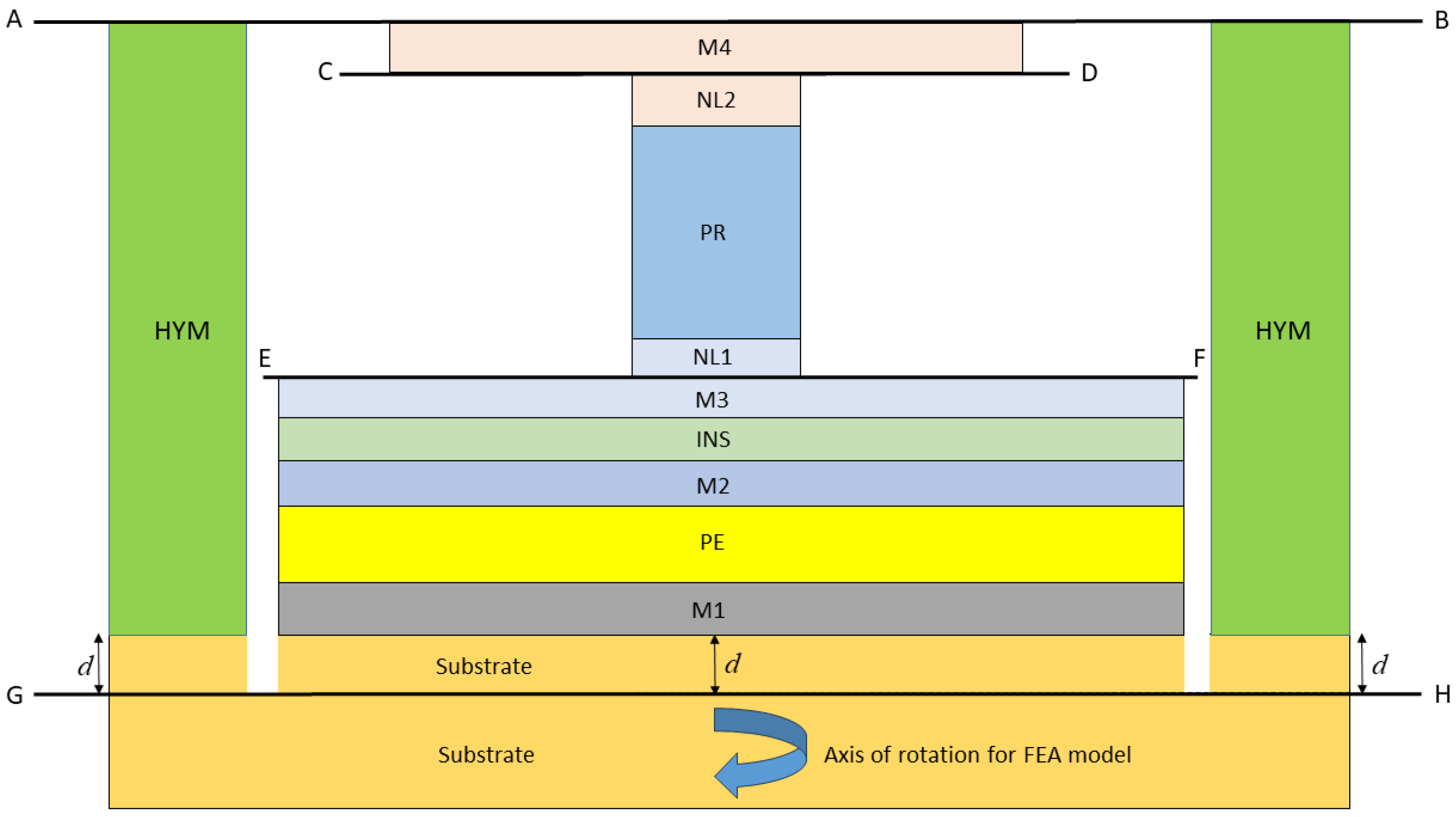
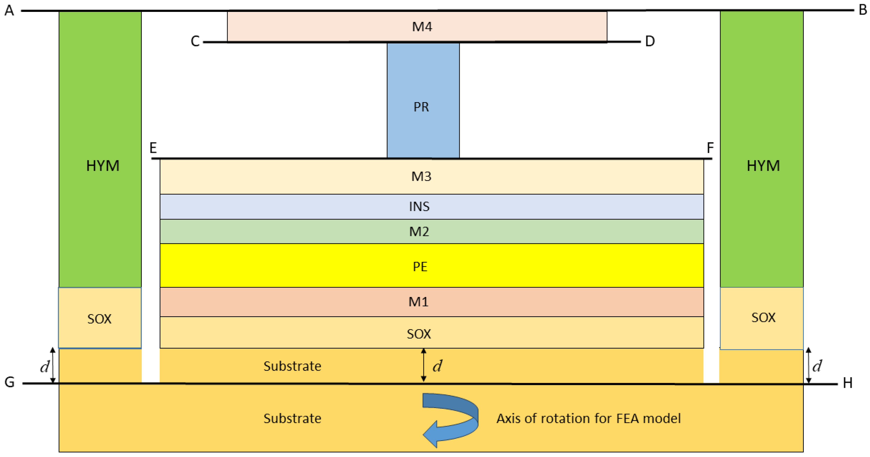
2. General Description and Material Properties for the Devices
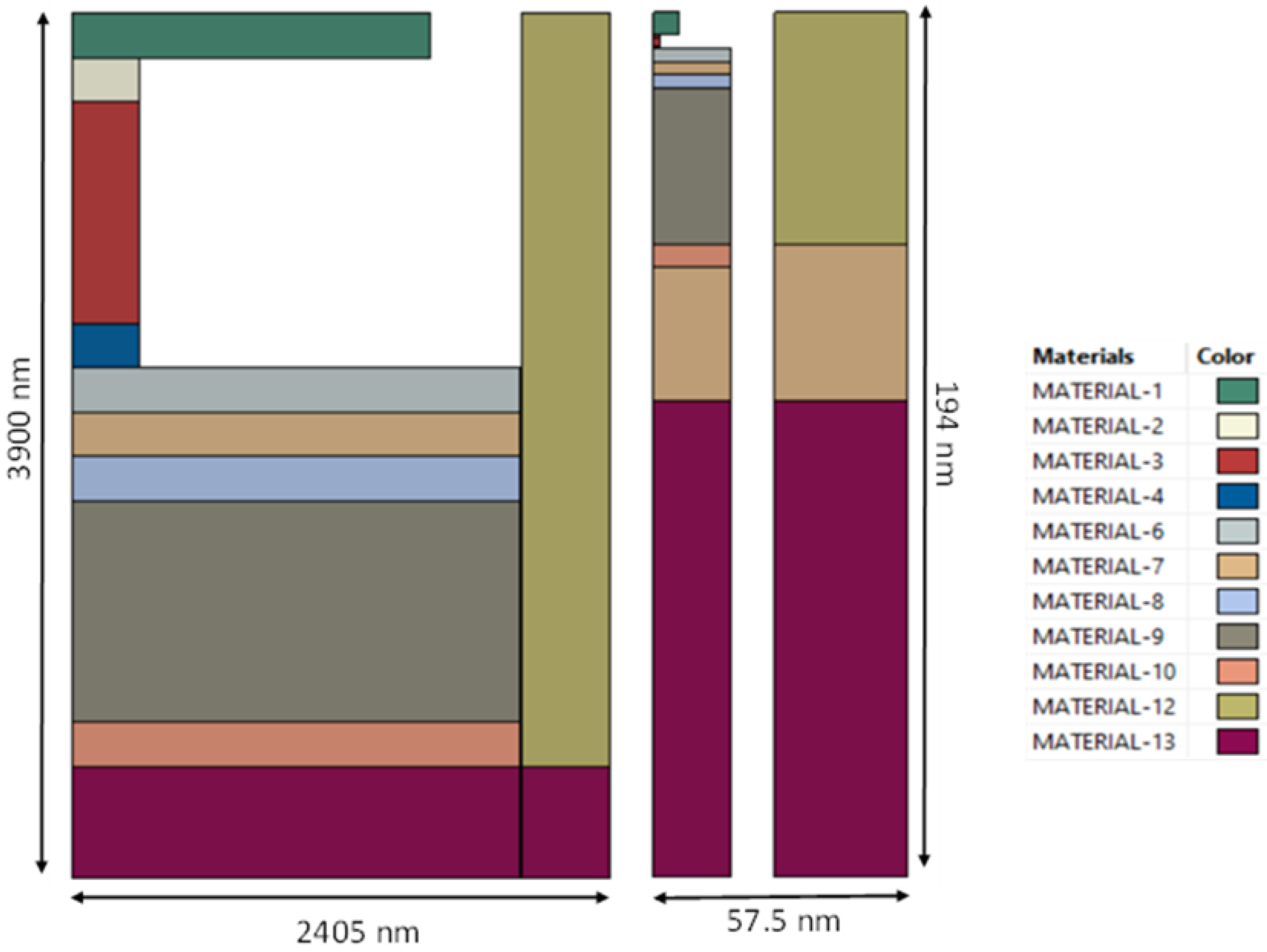
2.1. Dimensions and Isotropic Properties for Device Models
2.2. Anisotropic Properties
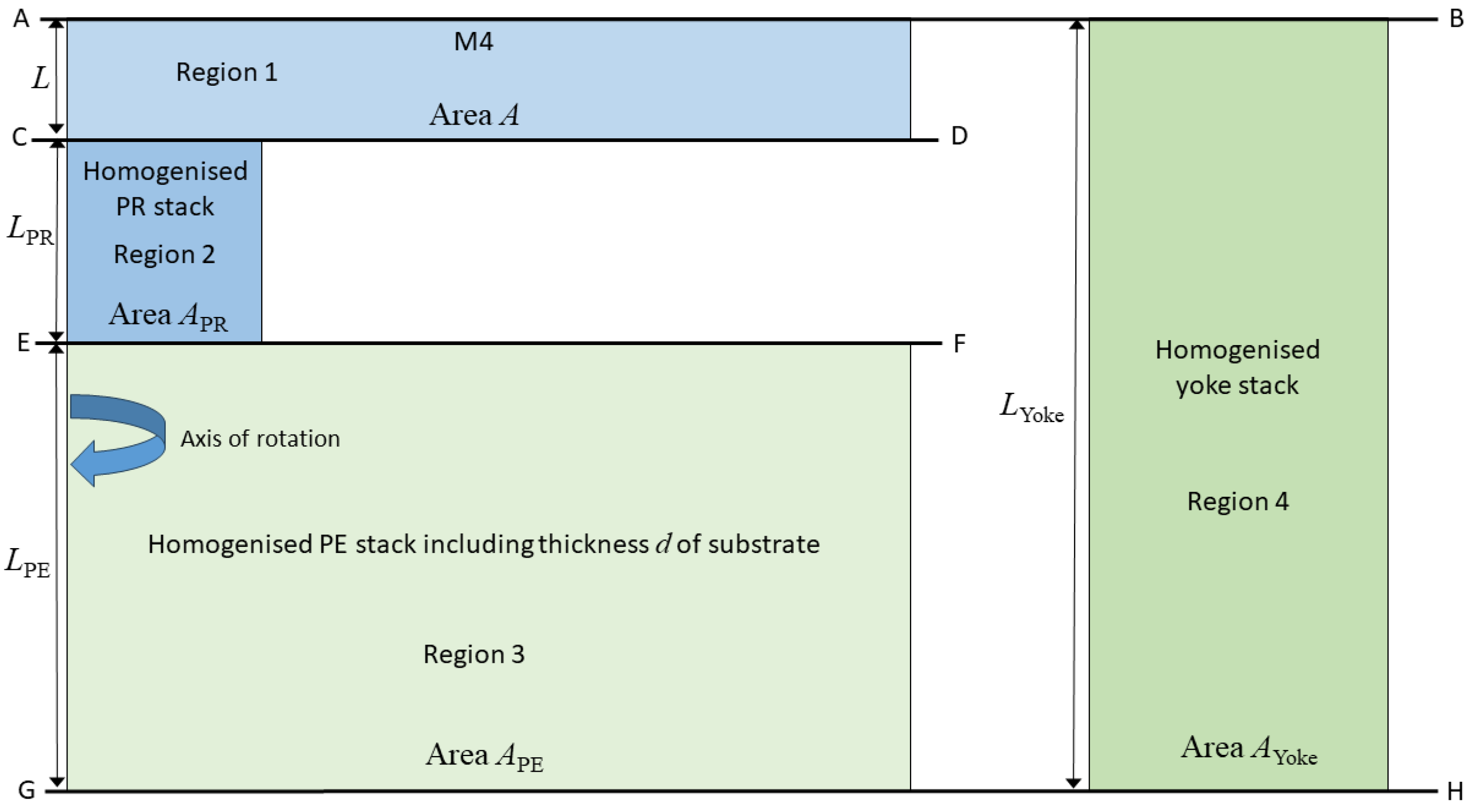
3. Development of an Equivalent 1D Model
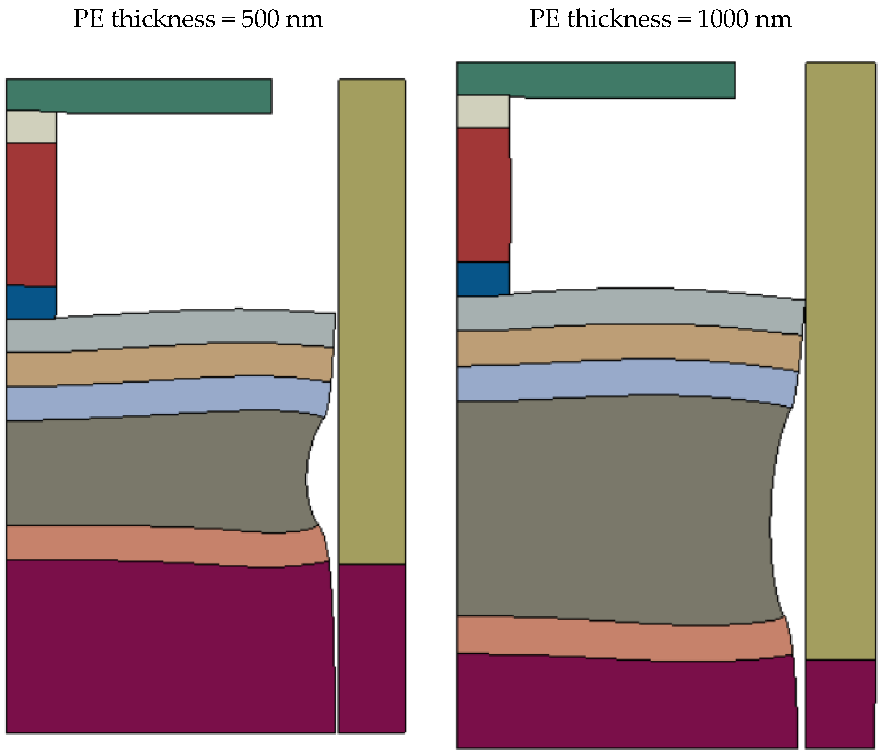
4. Finite Element Analysis
Constrained FEA Solutions for a Single Multi-Layered Stack
5. Results of Model Verification
6. Prediction of the Switching Voltages
6.1. Calculation of the Hydrostatic Pressure in the PR
6.2. Estimation of the Switching Voltage
7. Assessment of Device Performance Using the Compact Model and FEA Methods
8. Conclusions
Supplementary Materials
Author Contributions
Funding
Data Availability Statement
Acknowledgments
Conflicts of Interest
References
- McCartney, L.N.; Crocker, L.E.; Wright, L. Verification of a 3D analytical model of multi-layered piezoelectric systems using finite element analysis. J. Appl. Phys. 2019, 125, 184503. [Google Scholar] [CrossRef]
- McCartney, L.N.; Wright, L.; Cain, M.G.; Crain, J.; Martyna, G.J.; Newns, D.M. Methods for determining piezoelectric properties of thin epitaxial films: Theoretical foundations. J. Appl. Phys. 2014, 116, 014104. [Google Scholar] [CrossRef]
- Newns, D.M.; Elmegreen, B.; Liu, X.H.; Martyna, G.J. The piezoelectronic transistor: A nanoactuator-based post-CMOS digital switch with high speed and low power. MRS Bull. 2012, 37, 1071–1076. [Google Scholar] [CrossRef]
- Sugahara, S.; Shuto, Y.; Yamamoto, S.; Funakubo, H.; Kurosawa, M.K. Piezoelectronic transistor for low-voltage high-speed integrated electronics. In Proceedings of the 2017 IEEE SOI-3D Subthreshold Microelectronics Technology Unified Conference (S3S), Burlingame, CA, USA, 16–19 October 2017. [Google Scholar]
- Magdau, I.B.; Liu, X.H.; Kuroda, M.A.; Shaw, T.M.; Crain, J.; Solomon, P.M.; Newns, D.M.; Martyna, G.J. The piezoelectric stress transduction switch for very large scale integration, low voltage sensor computation, and radio frequency applications. Appl. Phys. Lett. 2015, 107, 073505. [Google Scholar] [CrossRef]
- Wortman, J.J.; Evans, R.A. Young’s modulus, shear modulus, and Poisson’s ratio in silicon and germanium. J. Appl. Phys. 1965, 36, 153–156. [Google Scholar] [CrossRef]
- Hopcroft, M.A.; Nix, W.D.; Kenny, T.W. What is the Young’s Modulus of Silicon? IEEE J. Microelectromech. Syst. 2010, 19, 229–238. Available online: http://www.silicon.mhopeng.ml1.net/Silicon/ (accessed on 23 December 2024). [CrossRef]
- Gupta, D.C.; Kulshrestha, S. Pressure induced magnetic, electronic and mechanical properties of SmX (X = Se, Te). J. Phys. Condens. Matter 2009, 21, 436011. [Google Scholar] [CrossRef] [PubMed]
- Zhang, R.; Jiang, B.; Cao, W. Elastic, piezoelectric and dielectric properties of multi-domain 0.67Pb(Mg1/3Nb2/3)O3-0.33PBTiO3 single crystals. J. Appl. Phys. 2001, 90, 3471–3475. [Google Scholar] [CrossRef]
- Abaqus 2021 User Documentation, Theory Manual © 2009–2021; Dassault Systèmes Simulia Corp.: Providence, RI, USA, 2021.
- Jayaraman, A.; Narayanamurti, V.; Bucher, E.; Maines, R.G. Continuous and Discontinuous Semiconductor-Metal Transition in Samarium Monochalcogenides Under Pressure. Phys. Rev. Lett. 1970, 25, 1430. [Google Scholar] [CrossRef]
- Jayaraman, A.; Maines, R.G. Study of the valence transition in Eu-, Yb-, and Ca-substituted SmS under high pressure and some comments on other substitutions. Phys. Rev. 1979, B19, 4145. [Google Scholar] [CrossRef]
- Horizon 2020 Project. Piezoelectronic Transduction Memory Device (PETMEM). Available online: https://cordis.europa.eu/project/id/688282/results (accessed on 23 December 2024).


| Layer Material | Outer Radius (nm) | Height (nm) | Young’s Modulus (GPa) | Poisson’s Ratio |
|---|---|---|---|---|
| M4 | 1600 | 200 | 200 | 0.25 |
| NL2 | 300 | 200 | 530 | 0.3 |
| PR | 300 | 1000 | Anisotropic | Anisotropic |
| NL1 | 300 | 200 | 530 | 0.3 |
| M3 | 2000 | 200 | 400 | 0.35 |
| INS | 2000 | 200 | 200 | 0.25 |
| M2 | 2000 | 200 | 530 | 0.3 |
| PE | 2000 | 1000 | Anisotropic | Anisotropic |
| M1 | 2000 | 200 | 170 | 0.38 |
| Substrate | 2000 | 500 (=d) | Anisotropic | Anisotropic |
| HYM | 2405 | 3400 | 530 | 0.3 |
| Yoke substrate | 2405 | 500 (=d) | Anisotropic | Anisotropic |
| Layer Material | Outer Radius (nm) | Height (nm) | Young’s Modulus (GPa) | Poisson’s Ratio |
|---|---|---|---|---|
| M4 (Ir) | 6 | 5 | 530 | 0.25 |
| PR (SmSe) | 1.5 | 3 | Anisotropic | Anisotropic |
| M3 (Ir) | 17.5 | 3 | 530 | 0.25 |
| INS (SiN) | 17.5 | 3 | 200 | 0.25 |
| M2 (Pt) | 17.5 | 3 | 170 | 0.38 |
| PE (PMN-Pt) | 17.5 | 35 | Anisotropic | Anisotropic |
| M1 (Pt) | 17.5 | 5 | 170 | 0.38 |
| SOX (SiN) | 17.5 | 30 | 200 | 0.25 |
| Substrate (Si [110]) | 17.5 | 107 (=d) | Anisotropic | Anisotropic |
| Yoke HYM (SiN) | 57.5 | 52 | 200 | 0.25 |
| Yoke SOX (SiN) | 57.5 | 35 | 200 | 0.25 |
| Yoke substrate (Si [110]) | 57.5 | 107 (=d) | Anisotropic | Anisotropic |
| Region | Compact Model (GPa) | FEA (GPa) | Magnitude of % Difference |
|---|---|---|---|
| M4 (top) | −1.2078517 × 10⁻³ | −1.20785297 × 10⁻³ | 1.05 × 10⁻⁴ |
| PR stack | −3.4356671 × 10⁻² | −3.43567021 × 10⁻² | 0.905 × 10⁻⁴ |
| PE stack | −7.7302509 × 10⁻⁴ | −7.73025968 × 10⁻⁴ | 1.14 × 10⁻⁴ |
| Yoke stack | 1.7528914 × 10⁻³ | 1.75289321 × 10⁻³ | 1.03 × 10⁻⁴ |
| Region | Compact Model (GPa) | FEA (GPa) | Magnitude of % Difference |
|---|---|---|---|
| M4 (top) | −0.54575555 | −0.54575551 | 8.06 × 10⁻⁶ |
| PR stack | −8.7320889 | −8.7320881 | 9.28 × 10⁻⁶ |
| PE stack | −0.064154122 | −0.064154133 | 1.75 × 10⁻⁵ |
| Yoke stack | 0.0077047843 | 0.0077047837 | 7.79 × 10⁻⁶ |
| Device (PE Layer Thickness) | Compact Model | FEA Model | Magnitude of % Difference |
|---|---|---|---|
| RF switch (500 nm) | 163.02204 V | 169.4606 V | 3.8 |
| RF switch (1000 nm) | 146.02465 V | 105.5251 V | 38.38 |
| VLSI device (35 nm) | 0.602725 V | 0.167211 V | 260 |
| VLSI device (70 nm) | 0.609608 V | 0.201502 V | 202 |
Disclaimer/Publisher’s Note: The statements, opinions and data contained in all publications are solely those of the individual author(s) and contributor(s) and not of MDPI and/or the editor(s). MDPI and/or the editor(s) disclaim responsibility for any injury to people or property resulting from any ideas, methods, instructions or products referred to in the content. |
© 2025 by the authors. Licensee MDPI, Basel, Switzerland. This article is an open access article distributed under the terms and conditions of the Creative Commons Attribution (CC BY) license (https://creativecommons.org/licenses/by/4.0/).
Share and Cite
McCartney, L.N.; Crocker, L.E.; Wright, L.; Rungger, I. A Compact Device Model for a Piezoelectric Nano-Transistor. Micromachines 2025, 16, 114. https://doi.org/10.3390/mi16020114
McCartney LN, Crocker LE, Wright L, Rungger I. A Compact Device Model for a Piezoelectric Nano-Transistor. Micromachines. 2025; 16(2):114. https://doi.org/10.3390/mi16020114
Chicago/Turabian StyleMcCartney, L. Neil, Louise E. Crocker, Louise Wright, and Ivan Rungger. 2025. "A Compact Device Model for a Piezoelectric Nano-Transistor" Micromachines 16, no. 2: 114. https://doi.org/10.3390/mi16020114
APA StyleMcCartney, L. N., Crocker, L. E., Wright, L., & Rungger, I. (2025). A Compact Device Model for a Piezoelectric Nano-Transistor. Micromachines, 16(2), 114. https://doi.org/10.3390/mi16020114