

Residual Stress and Warping Analysis of the Nano-Silver Pressureless Sintering Process in SiC Power Device Packaging
 ,
, 
Abstract
1. Introduction
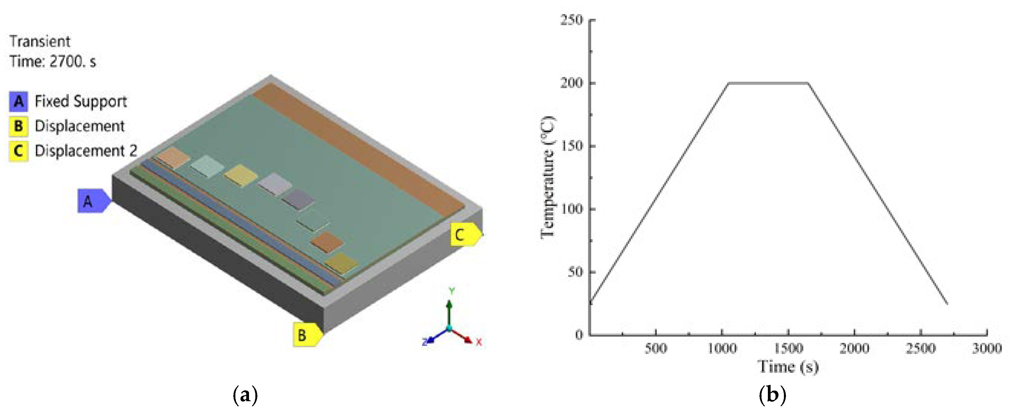
2. Model and Parameters
3. Effect of the Chip Sintering Process on Warpage and Residual Stress in the Power Modules
3.1. Warpage and Residual Stress Analysis in the Power Modules after Sintering
3.2. Effect of the Process Parameters on Warping and Residual Stress
3.3. Orthogonal Analysis of the Sintering Process Parameters
4. Conclusions
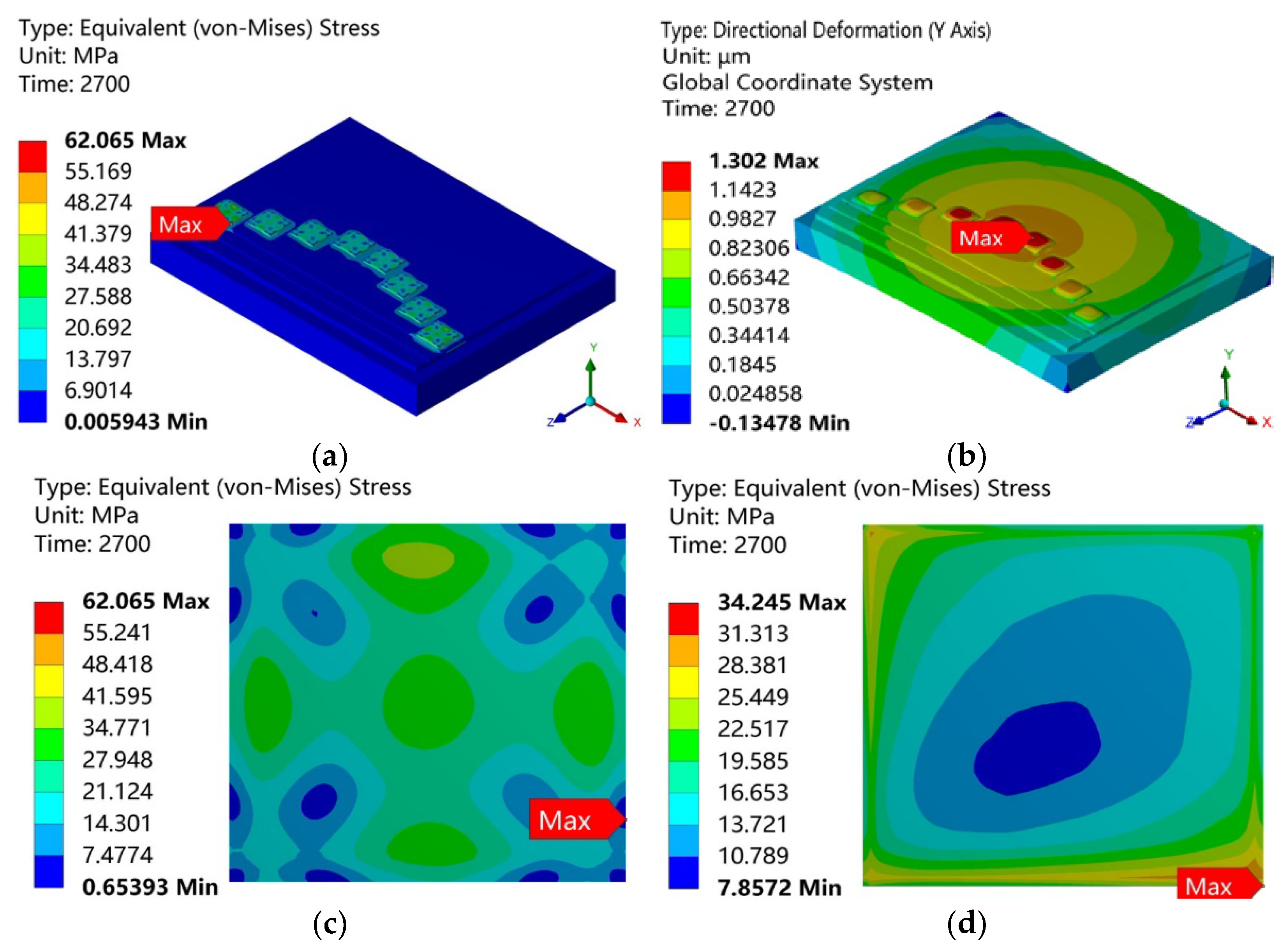
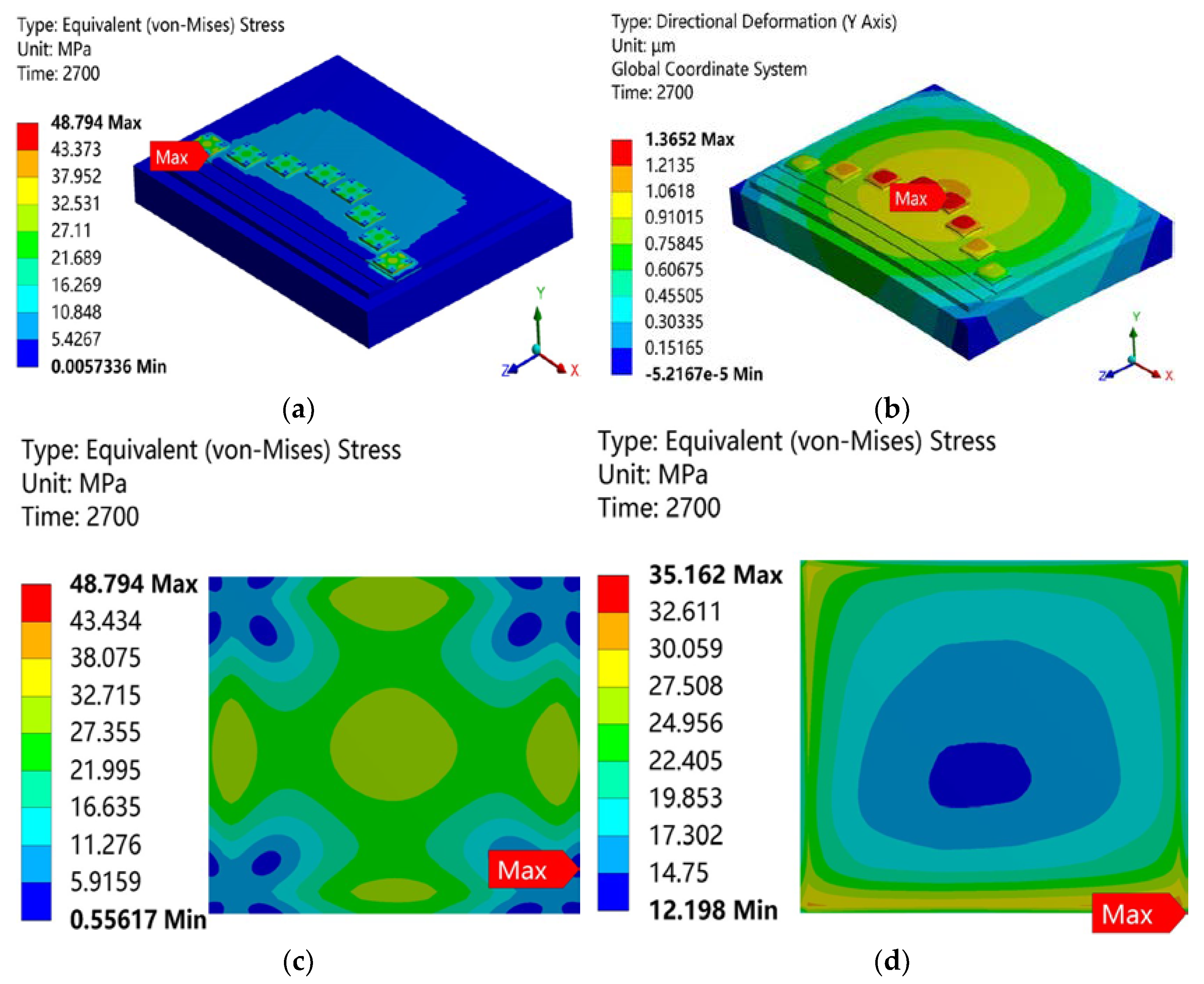
- After chip reflow welding, the power module as a whole showed convex warping. The maximum residual stress of the module appeared on the connection surface between the power chip and the solder paste layer. The stress distribution in the nano-silver solder paste layer increased from the center to the edges of the distribution circle, and the maximum residual stress appeared in the corners of the solder paste.
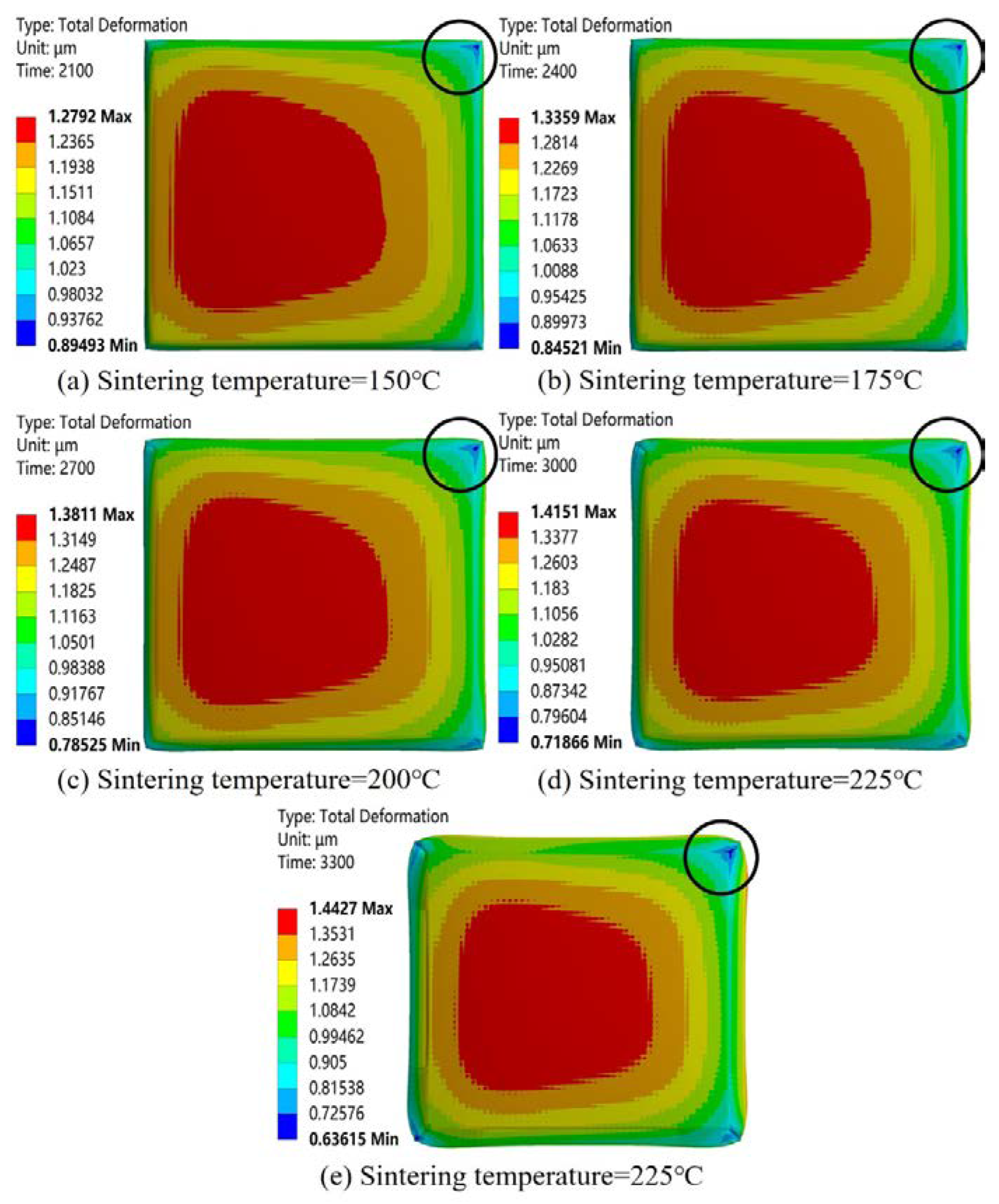
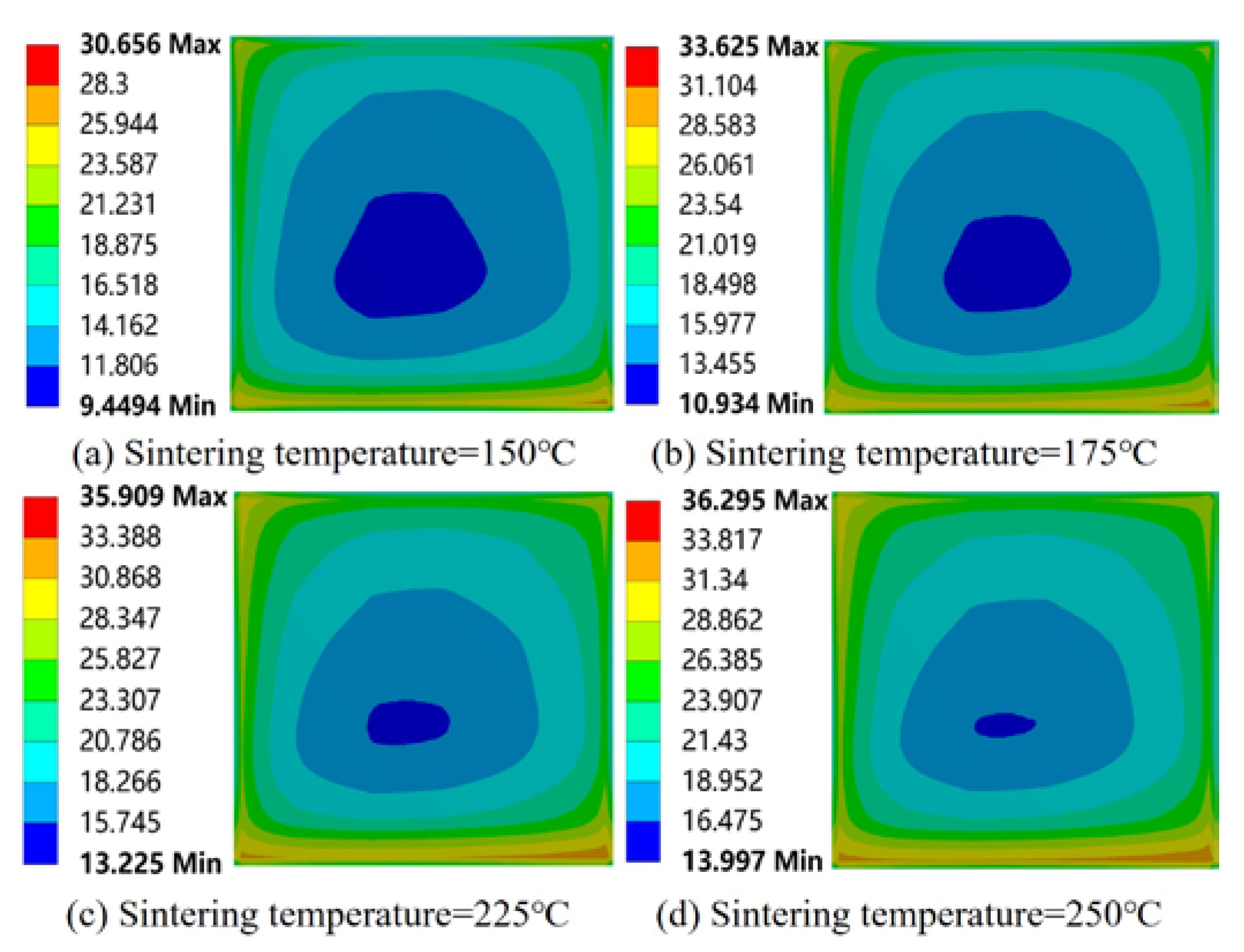
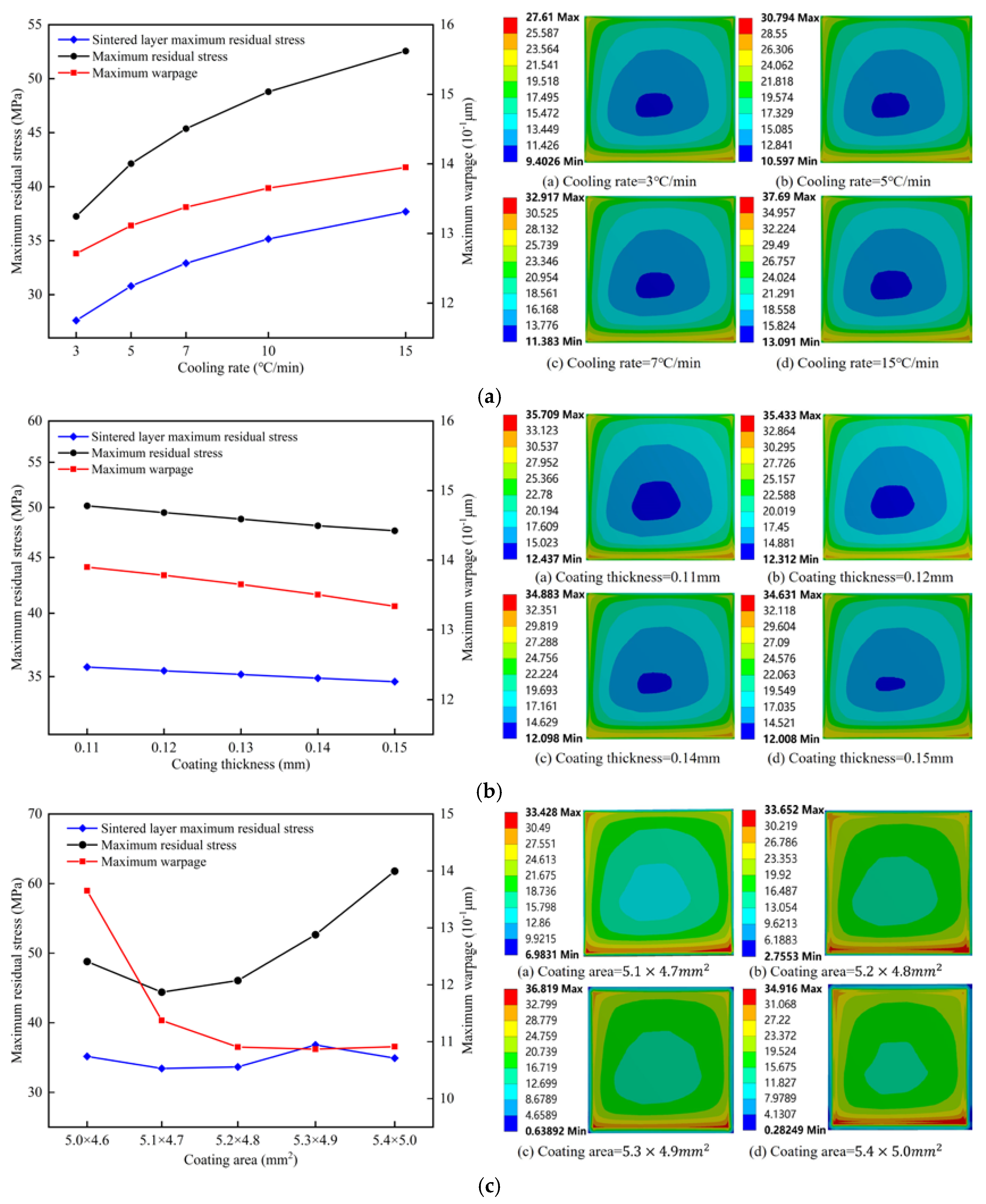
- The overall residual stress increased with the increase in sintering temperature and cooling rate. It decreased with the increase in coating thickness. It first decreased and then increased with the increase in coating area. Increasing the area and thickness of the solder paste layer could reduce the warping caused by the module in the chip welding process.
- The residual stress of the solder layer increased with the increase in sintering temperature and cooling rate. It decreased with the increase in coating thickness. With the increase in the coating area, it showed a wavy change.
- The orthogonal test analysis showed that the chip silver sintering process parameters can be classified in the following order with decreasing priority: sintering temperature, cooling rate, coating area, and coating thickness. The optimized chip welding parameters were as follows: the thickness of the solder paste was 0.14 mm, the area of the solder paste was 5.1 × 4.7 mm2, the sintering temperature was 150 °C, and the cooling rate was 5 °C/min. Under this optimal combination of the process parameters, the residual stress of the solder layer obtained by sintering was 24.83 MPa and was reduced by 29.38% compared with the original value of 35.162 MPa. This study provides a reference for selecting the process parameters of power module nano-silver sintering without pressure.
Author Contributions
Funding
Data Availability Statement
Conflicts of Interest
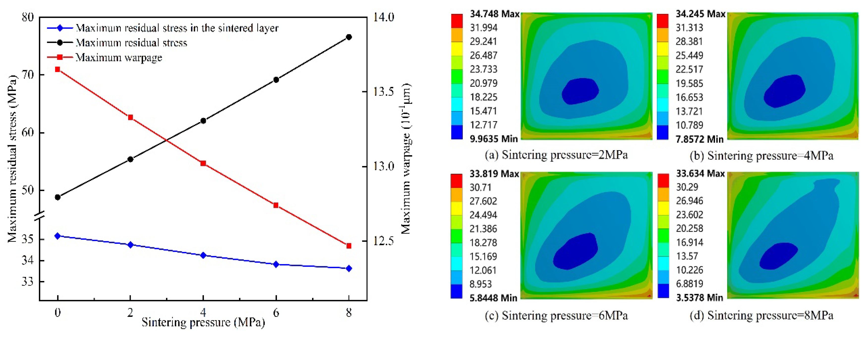
Appendix A. Pressure Sintering of Nano-Silver
Appendix B. Variation of the Solder Fillet Shape
References
- Tian, W.; Wu, S.; Li, W. Research of Vertical via Based on Silicon, Ceramic and Glass. Micromachines 2023, 14, 1391. [Google Scholar] [CrossRef] [PubMed]
- Tian, W.; Li, P.; Yuan, L. Research and analysis of MEMS switches in different frequency bands. Micromachines 2018, 9, 185. [Google Scholar] [CrossRef]
- Rafin, S.; Ahmed, R.; Haque, M.; Hossain, M.; Haque, M.; Mohammed, O. Power Electronics Revolutionized: A Comprehensive Analysis of Emerging Wide and Ultrawide Bandgap Devices. Micromachines 2023, 14, 2045. [Google Scholar] [CrossRef]
- Sheng, K.; Williams, B.W.; Finney, S.J. A review of IGBT models. IEEE Trans. Power Electron. 2000, 15, 1250–1266. [Google Scholar] [CrossRef]
- Yan, L.; Liu, P.; Xu, P.; Tan, L.; Zhang, Z. Reliability Analysis of Flip-Chip Packaging GaN Chip with Nano-Silver Solder BUMP. Micromachines 2023, 14, 1245. [Google Scholar] [CrossRef]
- Qian, J.; Shi, L.; Jin, M.; Bhattacharya, M.; Shimbori, A.; Yu, H.; Houshmand, S.; White, M.H.; Agarwal, A.K. An Investigation of Body Diode Reliability in Commercial 1.2 kV SiC Power MOSFETs with Planar and Trench Structures. Micromachines 2024, 15, 177. [Google Scholar] [CrossRef] [PubMed]
- Zhou, Y.; Xu, L.; Liu, S. Optimization for warpage and residual stress due to reflow process in IGBT modules based on pre-warped substrate. Microelectron. Eng. 2015, 136, 63–70. [Google Scholar] [CrossRef]
- Liu, Y. Power Electronic Packaging: Design, Assembly Process, Reliability and Modeling; Springer Science & Business Media: Berlin/Heidelberg, Germany, 2012. [Google Scholar]
- Deng, S.-S.; Hwang, S.-J.; Lee, H.-H. Temperature prediction for system in package assembly during the reflow soldering process. Int. J. Heat Mass Transf. 2016, 98, 1–9. [Google Scholar] [CrossRef]
- Siow, K.S. Are sintered silver joints ready for use as interconnect material in microelectronic packaging? J. Electron. Mater. 2014, 43, 947–961. [Google Scholar] [CrossRef]
- Xu, L.; Liu, Y.; Liu, S. Modeling and simulation of power electronic modules with microchannel coolers for thermo-mechanical performance. Microelectron. Reliab. 2014, 54, 2824–2835. [Google Scholar] [CrossRef]
- Addagarla, A.; Prasad, N.S. Finite element analysis of flip–chip on board (FCOB) assembly during reflow soldering process. Solder. Surf. Mt. Technol. 2012, 24, 92–99. [Google Scholar] [CrossRef]
- Kang, J.S. Parametric study of warpage in PBGA packages. Int. J. Adv. Manuf. Technol. 2020, 107, 4213–4219. [Google Scholar] [CrossRef]
- Liu, Y.; Zhang, H.; Wang, L.; Fan, X.; Zhang, G.; Sun, F. Stress analysis of pressure-assisted sintering for the double-side assembly of power module. Solder. Surf. Mt. Technol. 2019, 31, 20–27. [Google Scholar] [CrossRef]
- Bai, J.G.; Zhang, Z.Z.; Calata, J.N.; Lu, G.Q. Low-Temperature Sintered Nanoscale Silver as a Novel Semiconductor Device-Metallized Substrate Interconnect Material. IEEE Trans. Compon. Packag. Technol. 2006, 29, 589–593. [Google Scholar] [CrossRef]
- Tian, W.; Zhang, S.; Li, W.; Chen, Y.; Zhao, J.; Xin, F.; Qian, Y.; Li, W. Study on Cavitation, Warpage Deformation, and Moisture Diffusion of Sop-8 Devices during Molding Process. Micromachines 2023, 14, 2175. [Google Scholar] [CrossRef] [PubMed]
- Xu, H.; Huang, J.; Tian, W.; Li, Z. Thermal Performance Optimization of Integrated Microchannel Cooling Plate for IGBT Power Module. Micromachines 2023, 14, 1498. [Google Scholar] [CrossRef] [PubMed]
- Yu, D.-J.; Chen, X.; Chen, G.; Lu, G.-Q.; Wang, Z.-Q. Applying Anand model to low-temperature sintered nanoscale silver paste chip attachment. Mater. Des. 2009, 30, 4574–4579. [Google Scholar] [CrossRef]
- Brown, S.B.; Kim, K.H.; Anand, L. An internal variable constitutive model for hot working of metals. Int. J. Plast. 1989, 5, 95–130. [Google Scholar] [CrossRef]
- Chen, G.; Zhang, Z.-S.; Mei, Y.-H.; Li, X.; Yu, D.-J.; Wang, L.; Chen, X. Applying viscoplastic constitutive models to predict ratcheting behavior of sintered nanosilver lap-shear joint. Mech. Mater. 2014, 72, 61–71. [Google Scholar] [CrossRef]
- Gao, S.; Wang, R.; Wang, H.; Kang, R. Warping model of high-power IGBT modules subjected to reflow soldering process. Int. J. Mech. Sci. 2023, 251, 108350. [Google Scholar] [CrossRef]
- Sun, W.; Wang, L.; Zhu, N.; Xin, J.; Luo, Y.; Jiang, X.; Fan, G.; Chen, M. Characterization of packaging warpage, residual stress and their effects on the mechanical reliability of IGBT power modules. Eng. Fail. Anal. 2023, 152, 107517. [Google Scholar] [CrossRef]
- Fuste, N.; Avino, O.; Perpina, X.; Sanchez, D.; Vellvehi, M.; Jorda, X. Determination of Anand viscoplastic constitutive parameters for the AuGe solder alloy from experimental stress-strain curves for power systems integration FEA simulations. In Proceedings of the 2021 Smart Systems Integration (SSI), Grenoble, France, 27–29 April 2021; pp. 1–5. [Google Scholar]
- Haouala, S.; Doghri, I. Modeling and algorithms for two-scale time homogenization of viscoelastic-viscoplastic solids under large numbers of cycles. Int. J. Plast. 2015, 70, 98–125. [Google Scholar] [CrossRef]
- Holopainen, S.; Barriere, T.; Cheng, G.; Kouhia, R. Continuum approach for modeling fatigue in amorphous glassy polymers. Applications to the investigation of damage-ratcheting interaction in polycarbonate. Int. J. Plast. 2017, 91, 109–133. [Google Scholar] [CrossRef]
- Guo, Y.; Liu, M.; Yin, M.; Yan, Y. Reliability sensibility analysis of the PCB assembly concerning warpage during the reflow soldering process. Mathematics 2022, 10, 3055. [Google Scholar] [CrossRef]
- Li, J.; Johnson, C.M.; Buttay, C.; Sabbah, W.; Azzopardi, S. Bonding strength of multiple SiC die attachment prepared by sintering of Ag nanoparticles. J. Mater. Process. Technol. 2015, 215, 299–308. [Google Scholar] [CrossRef]
- Qi, K.; Chen, X.; Lu, G.Q. Effect of interconnection area on shear strength of sintered joint with nano-silver paste. Solder. Surf. Mt. Technol. 2008, 20, 8–12. [Google Scholar] [CrossRef]
- Lu, X.; Lv, Z.; Sun, Y.; Murugesan, M.; Zhou, C.; Zhang, X.; Liu, J. Enhanced Mechanical and Thermal Properties of Ag Joints Sintered by Spark Plasma Sintering. J. Electron. Mater. 2022, 51, 6310–6319. [Google Scholar] [CrossRef]


| Layer | Materials | Length (mm) | Width (mm) | Thickness (mm) |
|---|---|---|---|---|
| Colling baseplate | AlSiC | 60.0 | 45.0 | 6.0 |
| Baseplate solder layer | AuGe | 55.0 | 40.0 | 0.1 |
| Down copper | Cu | 55.0 | 40.0 | 0.3 |
| Ceramic layer | Si3N4 | 55.0 | 40.0 | 0.32 |
| Up copper | Cu | 55.0 | 28.0 | 0.3 |
| Chip solder layer | Nano-silver | 5.0 | 4.6 | 0.13 |
| IGBT chip | SiC | 5.0 | 4.6 | 0.36 |
| Materials | Density ρ (kg/m3) | Young’s Modulus E (GPa) | Poisson’s Ratio ν | CTE α (1 × 10⁻⁶/K) | Thermal Conductivity λ (W/m·K) | Specific Heat Capacity c (J/(kg·°C)) |
|---|---|---|---|---|---|---|
| SiC [22] | 3200 | 410 | 0.14 | 4.5 | 370 | 800 |
| Nano-silver [18] | 10500 | Table 3 | 0.37 | 19.6 | 240 | 234 |
| Cu [11] | 8950 | 110 | 0.34 | 16.4 | 385 | 385 |
| Si3N4 [17] | 3200 | 320 | 0.25 | 3 | 80 | 710 |
| AuGe [23] | 14670 | 68 | 0.32 | 13.4 | 44.4 | 130 |
| AlSiC [21] | 2960 | Table 5 | 0.4 | Table 5 | 200 | 750 |
| Temperature (°C) | 25 | 60 | 120 | 150 | 250 |
|---|---|---|---|---|---|
| Young’s modulus (GPa) | 6.28 | 4.52 | 2.64 | 1.58 | 0.5 |
| Parameters | Value | Definition |
|---|---|---|
| S0 (MPa) | 2.93 | Initial value of deformation resistance |
| Q/R (K) | 5706.3 | Activation energy/Boltzmann constant |
| A (1/s) | 9.81 | Pre-exponential factor |
| ξ | 12 | Stress multiplier |
| m | 0.6572 | Strain rate sensitivity of stress |
| h0 (MPa) | 14600 | Hardening coefficient |
| ŝ (MPa) | 101.7 | Coefficient for deformation resistance saturation value |
| n | 0.00326 | Strain rate sensitivity of saturation value |
| α | 1 | Strain rate sensitivity of hardening coefficient |
| Temperature (°C) | Young’s Modulus (GPa) | CTE(1E-6/K) |
|---|---|---|
| 50 | 192.68 | 3.65 |
| 100 | 189.74 | 5.67 |
| 150 | 183.26 | 6.59 |
| 200 | 178.70 | 7.16 |
| 250 | 176.19 | 7.48 |
| 300 | 167.81 | 7.62 |
| Serial Number | Sintering Temperature (°C) | Heating Rate (°C/min) | Nano-Silver Thickness (mm) | Nano-Silver Area (mm2) |
|---|---|---|---|---|
| 1 | 150 | 10 | 0.13 | 5.0 × 4.6 |
| 2 | 175 | 10 | 0.13 | 5.0 × 4.6 |
| 3 | 200 | 10 | 0.13 | 5.0 × 4.6 |
| 4 | 225 | 10 | 0.13 | 5.0 × 4.6 |
| 5 | 250 | 10 | 0.13 | 5.0 × 4.6 |
| 6 | 200 | 10 | 0.13 | 5.0 × 4.6 |
| 7 | 200 | 10 | 0.13 | 5.0 × 4.6 |
| 8 | 200 | 10 | 0.13 | 5.0 × 4.6 |
| 9 | 200 | 10 | 0.13 | 5.0 × 4.6 |
| 10 | 200 | 10 | 0.13 | 5.0 × 4.6 |
| 11 | 200 | 3 | 0.13 | 5.0 × 4.6 |
| 12 | 200 | 5 | 0.13 | 5.0 × 4.6 |
| 13 | 200 | 7 | 0.13 | 5.0 × 4.6 |
| 14 | 200 | 10 | 0.13 | 5.0 × 4.6 |
| 15 | 200 | 15 | 0.13 | 5.0 × 4.6 |
| 16 | 200 | 10 | 0.11 | 5.0 × 4.6 |
| 17 | 200 | 10 | 0.12 | 5.0 × 4.6 |
| 18 | 200 | 10 | 0.13 | 5.0 × 4.6 |
| 19 | 200 | 10 | 0.14 | 5.0 × 4.6 |
| 20 | 200 | 10 | 0.15 | 5.0 × 4.6 |
| 21 | 200 | 10 | 0.13 | 5.0 × 4.6 |
| 22 | 200 | 10 | 0.13 | 5.1 × 4.7 |
| 23 | 200 | 10 | 0.13 | 5.2 × 4.8 |
| 24 | 200 | 10 | 0.13 | 5.3 × 4.9 |
| 25 | 200 | 10 | 0.13 | 5.4 × 5.0 |
| Factor Level | A (mm) | B (mm2) | C (°C) | D (°C/min) |
|---|---|---|---|---|
| 1 | 0.15 | 5.2 × 4.8 | 200 | 10 |
| 2 | 0.14 | 5.1 × 4.7 | 175 | 7 |
| 3 | 0.13 | 5.0 × 4.6 | 150 | 5 |
| Test Number | Factor | Maximum Residual Stress (MPa) | |||
|---|---|---|---|---|---|
| A | B | C | D | ||
| 1 | 0.15 | 5.2 × 4.8 | 200 | 10 | 32.723 |
| 2 | 0.15 | 5.1 × 4.7 | 175 | 7 | 28.616 |
| 3 | 0.15 | 5.0 × 4.6 | 150 | 5 | 27.172 |
| 4 | 0.14 | 5.2 × 4.8 | 175 | 5 | 27.691 |
| 5 | 0.14 | 5.1 × 4.7 | 150 | 10 | 27.783 |
| 6 | 0.14 | 5.0 × 4.6 | 200 | 7 | 32.668 |
| 7 | 0.13 | 5.2 × 4.8 | 150 | 7 | 27.116 |
| 8 | 0.13 | 5.1 × 4.7 | 200 | 5 | 29.116 |
| 9 | 0.13 | 5.0 × 4.6 | 175 | 10 | 33.625 |
| K1 | 88.511 | 87.530 | 94.507 | 94.131 | |
| K2 | 88.142 | 85.515 | 89.932 | 88.400 | |
| K3 | 89.857 | 93.465 | 82.071 | 83.979 | |
| k1 | 29.504 | 29.177 | 31.502 | 31.377 | |
| k2 | 29.381 | 28.505 | 29.977 | 29.467 | |
| k3 | 29.952 | 31.155 | 27.357 | 27.993 | |
| Ri | 0.572 | 2.650 | 4.145 | 3.384 | |
| Sequence | C > D > B > A | ||||
| Optimal combination | A2B2C3D3 | 24.83 | |||
Disclaimer/Publisher’s Note: The statements, opinions and data contained in all publications are solely those of the individual author(s) and contributor(s) and not of MDPI and/or the editor(s). MDPI and/or the editor(s) disclaim responsibility for any injury to people or property resulting from any ideas, methods, instructions or products referred to in the content. |
© 2024 by the authors. Licensee MDPI, Basel, Switzerland. This article is an open access article distributed under the terms and conditions of the Creative Commons Attribution (CC BY) license (https://creativecommons.org/licenses/by/4.0/).
Share and Cite
Tian, W.; Li, D.; Dang, H.; Liang, S.; Zhang, Y.; Zhang, X.; Chen, S.; Yu, X. Residual Stress and Warping Analysis of the Nano-Silver Pressureless Sintering Process in SiC Power Device Packaging. Micromachines 2024, 15, 1087. https://doi.org/10.3390/mi15091087
Tian W, Li D, Dang H, Liang S, Zhang Y, Zhang X, Chen S, Yu X. Residual Stress and Warping Analysis of the Nano-Silver Pressureless Sintering Process in SiC Power Device Packaging. Micromachines. 2024; 15(9):1087. https://doi.org/10.3390/mi15091087
Chicago/Turabian StyleTian, Wenchao, Dexin Li, Haojie Dang, Shiqian Liang, Yizheng Zhang, Xiaojun Zhang, Si Chen, and Xiaochuan Yu. 2024. "Residual Stress and Warping Analysis of the Nano-Silver Pressureless Sintering Process in SiC Power Device Packaging" Micromachines 15, no. 9: 1087. https://doi.org/10.3390/mi15091087
APA StyleTian, W., Li, D., Dang, H., Liang, S., Zhang, Y., Zhang, X., Chen, S., & Yu, X. (2024). Residual Stress and Warping Analysis of the Nano-Silver Pressureless Sintering Process in SiC Power Device Packaging. Micromachines, 15(9), 1087. https://doi.org/10.3390/mi15091087