
A CMOS-Compatible Process for ≥3 kV GaN Power HEMTs on 6-inch Sapphire Using In Situ SiN as the Gate Dielectric

Abstract
1. Introduction
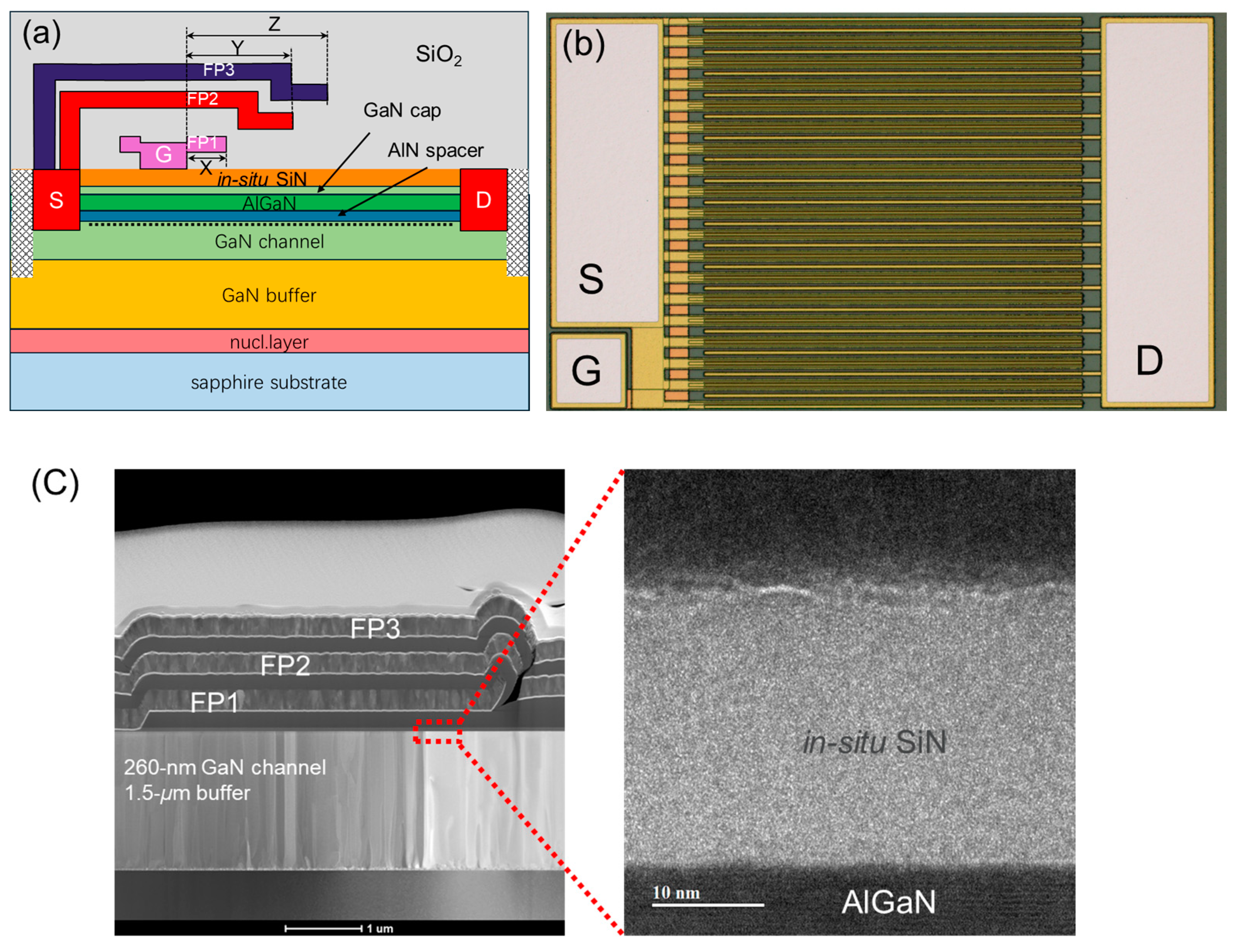
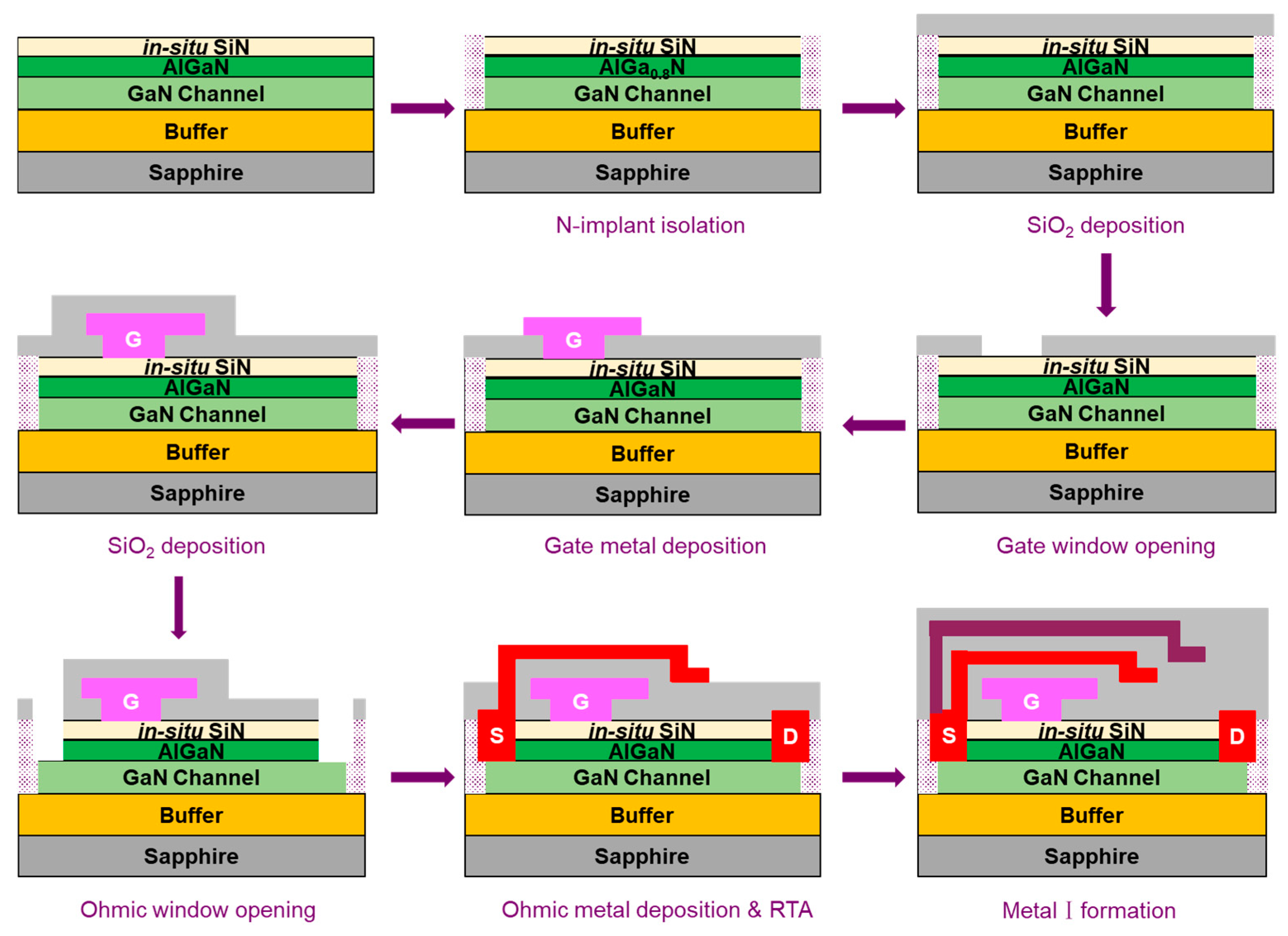
2. Materials and Methods
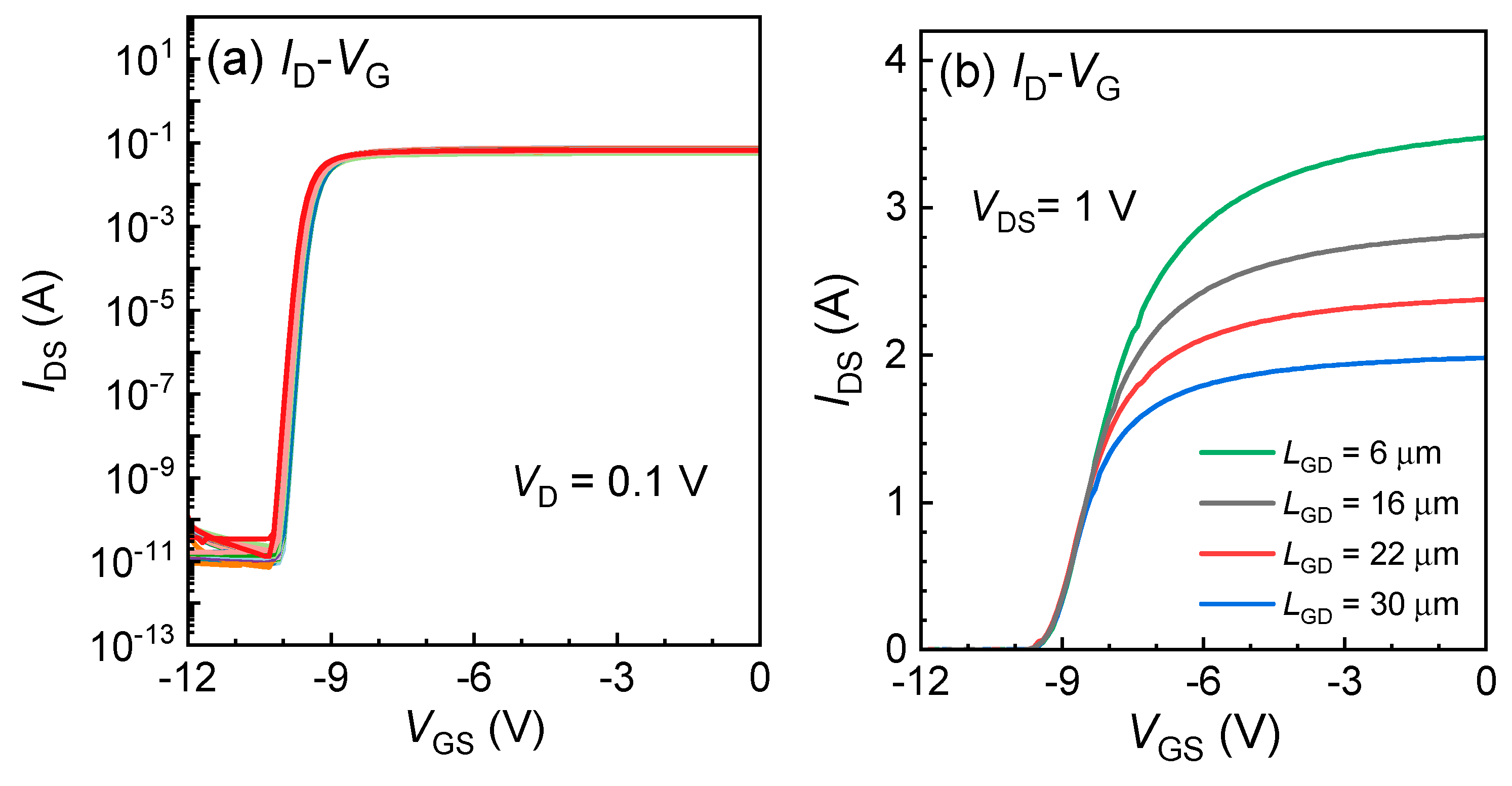
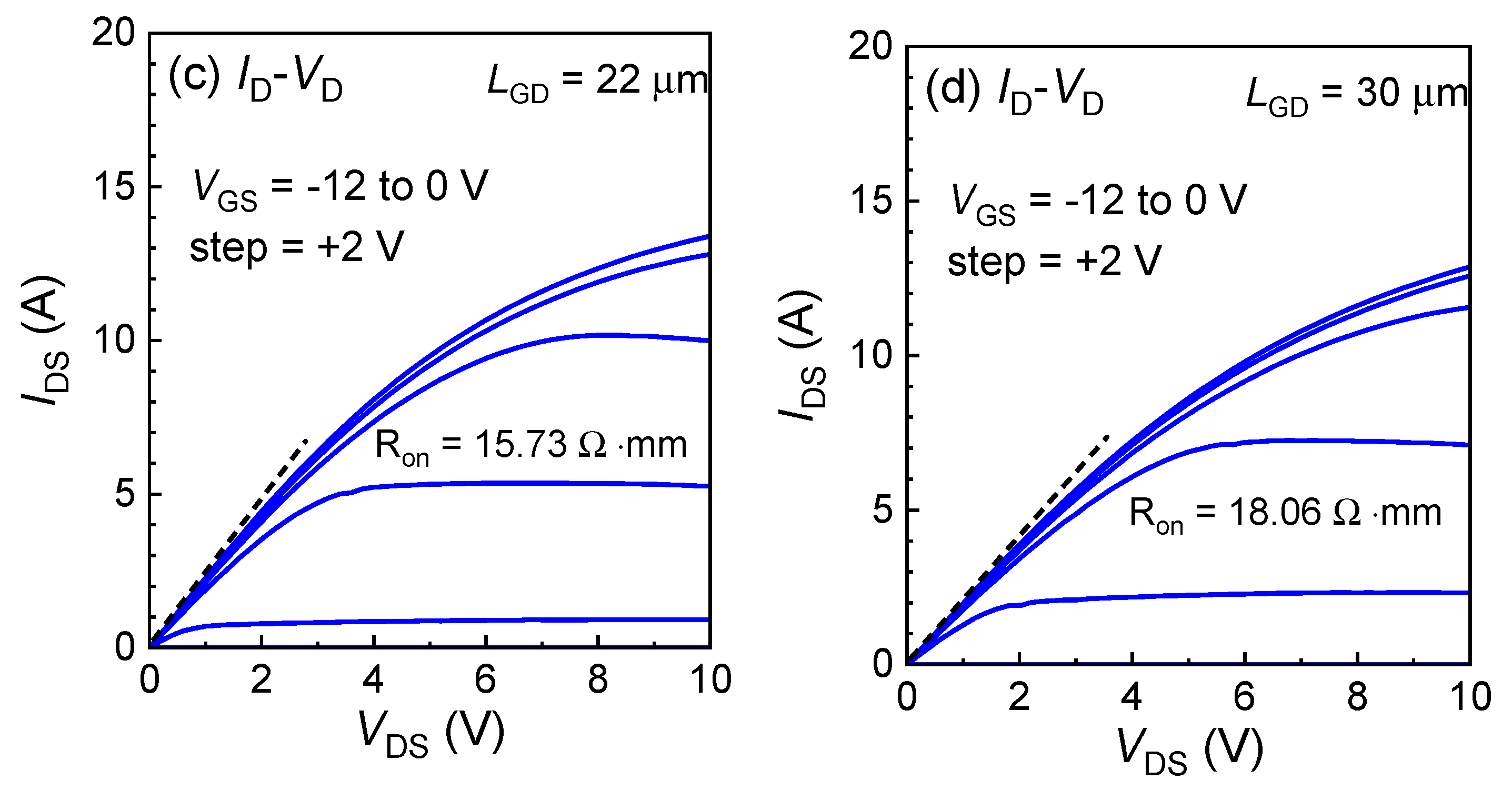
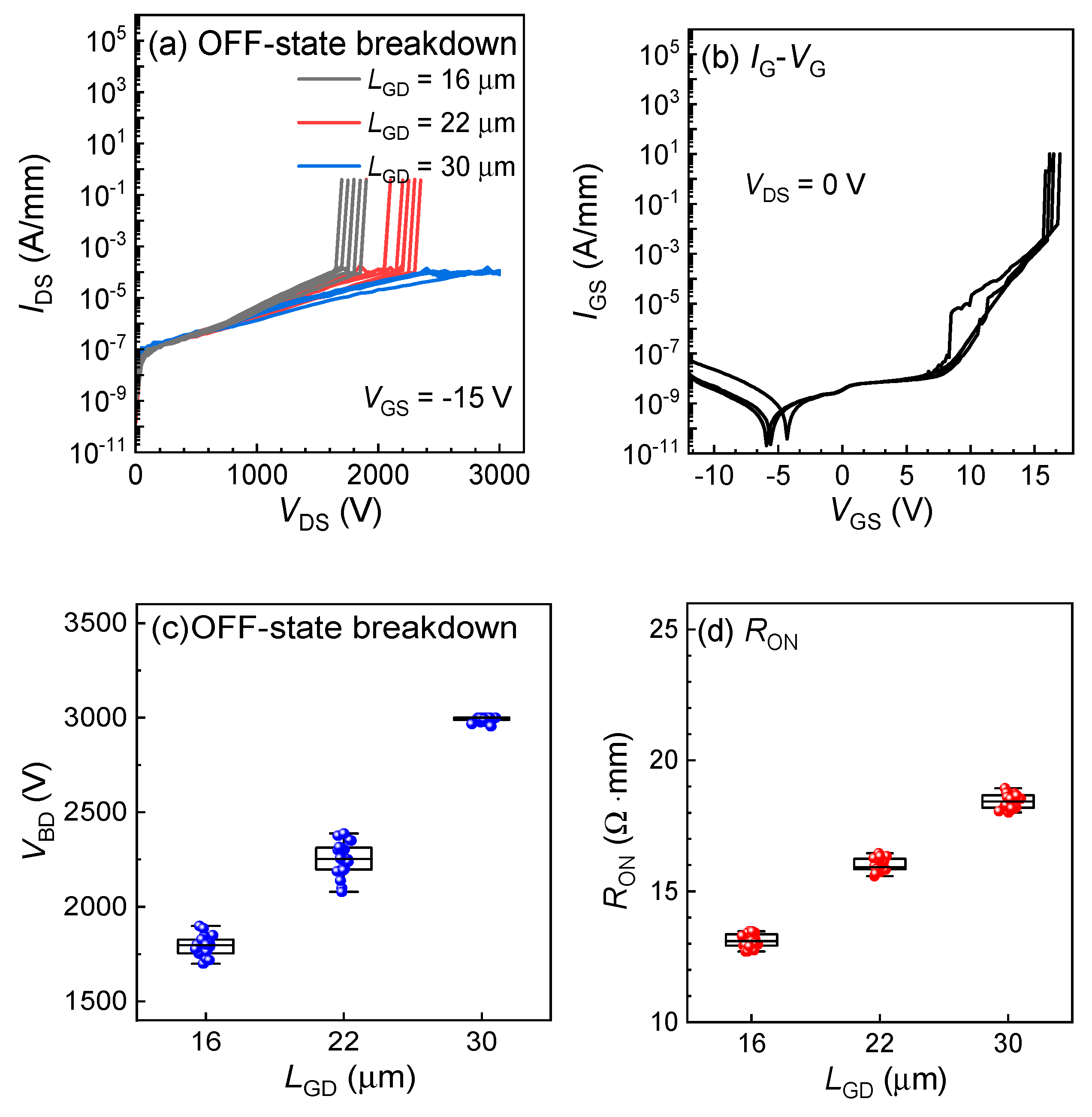
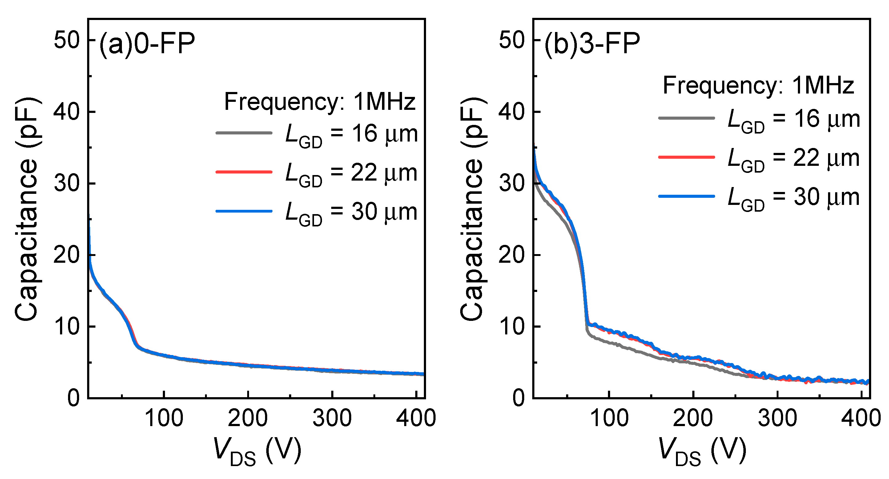
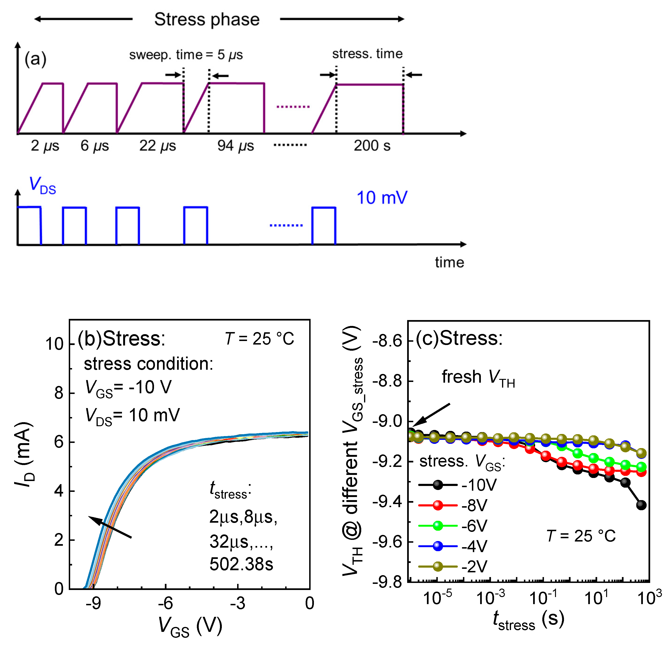
3. Results
4. Conclusions
Author Contributions
Funding
Data Availability Statement
Acknowledgments
Conflicts of Interest
References
- Jones, E.A.; Wang, F.F.; Costinett, D. Review of Commercial GaN Power Devices and GaN-Based Converter Design Challenges. IEEE J. Emerg. Sel. Top. Power Electron. 2016, 4, 707–719. [Google Scholar] [CrossRef]
- Amano, H.; Baines, Y.; Beam, E.; Borga, M.; Bouchet, T.; Chalker, P.R.; Charles, M.; Chen, K.J.; Chowdhury, N.; Chu, R.; et al. The 2018 GaN power electronics roadmap. J. Phys. D Appl. Phys. 2018, 51, 163001. [Google Scholar] [CrossRef]
- Chen, K.J.; Haberlen, O.; Lidow, A.; lin Tsai, C.; Ueda, T.; Uemoto, Y.; Wu, Y. GaN-on-Si power technology: Devices and applications. IEEE Trans. Electron. Devices 2017, 64, 779–795. [Google Scholar] [CrossRef]
- Hoo Teo, K.; Zhang, Y.; Chowdhury, N.; Rakheja, S.; Ma, R.; Xie, Q.; Palacios, T. Emerging GaN technologies for power, RF, digital, and quantum computing applications: Recent advances and prospects. J. Appl. Phys. 2021, 130, 160902. [Google Scholar] [CrossRef]
- Islam, N.; Mohamed, M.F.P.; Khan, M.F.A.J.; Falina, S.; Kawarada, H.; Syamsul, M. Reliability, applications and challenges of GaN HEMT technology for modern power devices: A review. Crystals 2022, 12, 1581. [Google Scholar] [CrossRef]
- Flack, T.J.; Pushpakaran, B.N.; Bayne, S.B. GaN Technology for Power Electronic Applications: A Review. J. Electron. Mater. 2016, 45, 2673–2682. [Google Scholar] [CrossRef]
- Wang, J.; Zhao, T.; Li, J.; Huang, A.Q.; Callanan, R.; Husna, F.; Agarwal, A. Characterization, modeling, and application of 10-kV SiC MOSFET. IEEE Trans. Electron. Devices 2008, 55, 1798–1806. [Google Scholar] [CrossRef]
- Huang, X.; Liu, Z.; Lee, F.C.; Li, Q. Characterization and Enhancement of High-Voltage Cascode GaN Devices. IEEE Trans. Electron. Devices 2015, 62, 270–277. [Google Scholar] [CrossRef]
- Stoffels, S.; Zhao, M.; Venegas, R.; Kandaswamy, P.; You, S.; Novak, T.; Decoutere, S. The physical mechanism of dispersion caused by AlGaN/GaN buffers on Si and optimization for low dispersion. In Proceedings of the 2015 IEEE International Electron Devices Meeting, Washington, DC, USA, 7–9 December 2015; pp. 35.4.1–35.4.4. [Google Scholar] [CrossRef]
- Ishida, M.; Ueda, T.; Tanaka, T.; Ueda, D. GaN on Si technologies for power switching devices. IEEE Trans. Electron. Devices 2013, 60, 3053–3059. [Google Scholar] [CrossRef]
- Selvaraj, S.L.; Suzue, T.; Egawa, T. Breakdown enhancement of AlGaN/GaN HEMTs on 4-in silicon by improving the GaN quality on thick buffer layers. IEEE Electron. Device Lett. 2009, 30, 587–589. [Google Scholar] [CrossRef]
- Able, A.; Wegscheider, W.; Engl, K.; Zweck, J. Growth of crack-free GaN on Si(1 1 1) with graded AlGaN buffer layers. J. Cryst. Growth 2005, 276, 415–418. [Google Scholar] [CrossRef]
- Musolino, M.; Xu, X.; Wang, H.; Rengarajan, V.; Zwieback, I.; Ruland, G.; Messina, A. Paving the way toward the world’s first 200 mm SiC pilot line. Mater. Sci. Semicond. Process. 2021, 135, 106088. [Google Scholar] [CrossRef]
- Hult, B.; Thorsell, M.; Chen, J.T.; Rorsman, N. High Voltage and Low Leakage GaN-on-SiC MISHEMTs on a “Buffer-Free” Heterostructure. IEEE Electron. Device Lett. 2022, 43, 781–784. [Google Scholar] [CrossRef]
- Jiang, Q.; Liu, C.; Lu, Y.; Chen, K.J. High-voltage enhancement/Depletion-mode AlGaN/GaN HEMTs on modified SOI substrates. In Proceedings of the 2013 25th International Symposium on Power Semiconductor Devices & IC’s (ISPSD), Kanazawa, Japan, 26–30 May 2013; pp. 407–410. [Google Scholar] [CrossRef]
- Li, X.; Geens, K.; Guo, W.; You, S.; Zhao, M.; Fahle, D.; Decoutere, S. Demonstration of GaN integrated half-bridge with on-chip drivers on 200- mm engineered substrates. IEEE Electron. Device Lett. 2019, 40, 1499–1502. [Google Scholar] [CrossRef]
- Integrations, P. InnoSwitch3-CE Family Datasheet. 2023. Available online: https://www.powerint.cn/sites/default/files/documents/innoswitch3-ce_family_datasheet.pdf (accessed on 10 June 2024).
- KYOCERA. Single-Crystal Sapphire Datasheet. 2022. Available online: https://global.kyocera.com/prdct/fc/product/pdf/s_c_sapphire.pdf (accessed on 11 June 2024).
- Gupta, G.; Kanamura, M.; Swenson, B.; Neufeld, C.; Hosoda, T.; Parikh, P.; Mishra, U. 1200V GaN Switches on Sapphire: A low-cost, high-performance platform for EV and industrial applications. In Proceedings of the 2022 International Electron Devices Meeting (IEDM), San Francisco, CA, USA, 3–7 December 2022; pp. 35.2.1–35.2.4. [Google Scholar] [CrossRef]
- Cui, J.; Wu, Y.; Yang, J.; Yu, J.; Li, T.; Yang, X.; Wei, J. Method to Study Dynamic Depletion Behaviors in High-Voltage (BV = 1.4 kV) p-GaN Gate HEMT on Sapphire Substrate. In Proceedings of the 2023 35th International Symposium on Power Semiconductor Devices and ICs (ISPSD), Hong Kong, China, 28 May–1 June 2023; pp. 127–130. [Google Scholar] [CrossRef]
- Li, X.; Wang, J.; Zhang, J.; Han, Z.; You, S.; Chen, L.; Hao, Y. 1700 V High-performance GaN HEMTs on 6-inch Sapphire with 1.5 μm Thin Buffer. IEEE Electron. Device Lett. 2023, 45, 84–87. [Google Scholar] [CrossRef]
- Li, X.; Zhang, J.; Ji, J.; Cheng, Z.; Wang, J.; Chen, L.; Zhang, J. Demonstration of >8-kV GaN HEMTs with CMOS-compatible manufacturing on 6-in sapphire substrates for medium-voltage applications. IEEE Trans. Electron. Devices 2024, 71, 3989–3993. [Google Scholar] [CrossRef]
- Han, Z.; Li, X.; Ji, J.; Chen, L.; Wang, L.; Cheng, Z.; Zhang, J. p-GaN Gate HEMTs on 6-inch Sapphire by CMOS-Compatible Process: A Promising Game Changer for Power Electronics. IEEE Electron. Device Lett. 2024, 45, 1257–1260. [Google Scholar] [CrossRef]
- Wang, J.; Li, X.; Chen, L.; Liu, T.; Han, Z.; You, S.; Zhang, J. Report of GaN HEMTs on 8-in Sapphire. IEEE Trans. Electron. Devices 2024, 71, 4429–4432. [Google Scholar] [CrossRef]
- Li, S.; Ma, Y.; Lu, W.; Li, M.; Wang, L.; Zhang, Z.; Sun, W. 1200 V E-mode GaN monolithic integration platform on sapphire with ultra-thin buffer technology. In Proceedings of the 2023 International Electron Devices Meeting (IEDM), San Francisco, CA, USA, 9–13 December 2023; p. 9. [Google Scholar] [CrossRef]
- Lu, W.; Li, S.; Liu, S.; Ma, Y.; Zhang, L.; Wei, J.; Zhu, T. Superior Performances of Dynamic On-State Resistance in 1.9 kV GaN-on-Sapphire HEMT. In Proceedings of the 2023 IEEE International Conference on Integrated Circuits, Technologies and Applications, Hefei, China, 27–29 October 2023; pp. 13–14. [Google Scholar] [CrossRef]
- Guo, A.; del Alamo, J.A. Unified mechanism for positive-and negative-bias temperature instability in GaN MOSFETs. IEEE Trans. Electron. Devices 2017, 64, 2142–2147. [Google Scholar] [CrossRef]
- Van Hove, M.; Boulay, S.; Bahl, S.R.; Stoffels, S.; Kang, X.; Wellekens, D.; Decoutere, S. CMOS process-compatible high-power low-leakage AlGaN/GaN MISHEMT on silicon. IEEE Electron Device Lett. 2012, 33, 667–669. [Google Scholar] [CrossRef]


Disclaimer/Publisher’s Note: The statements, opinions and data contained in all publications are solely those of the individual author(s) and contributor(s) and not of MDPI and/or the editor(s). MDPI and/or the editor(s) disclaim responsibility for any injury to people or property resulting from any ideas, methods, instructions or products referred to in the content. |
© 2024 by the authors. Licensee MDPI, Basel, Switzerland. This article is an open access article distributed under the terms and conditions of the Creative Commons Attribution (CC BY) license (https://creativecommons.org/licenses/by/4.0/).
Share and Cite
Zhang, J.; Li, X.; Ji, J.; You, S.; Chen, L.; Wang, L.; Li, Z.; Hao, Y.; Zhang, J. A CMOS-Compatible Process for ≥3 kV GaN Power HEMTs on 6-inch Sapphire Using In Situ SiN as the Gate Dielectric. Micromachines 2024, 15, 1005. https://doi.org/10.3390/mi15081005
Zhang J, Li X, Ji J, You S, Chen L, Wang L, Li Z, Hao Y, Zhang J. A CMOS-Compatible Process for ≥3 kV GaN Power HEMTs on 6-inch Sapphire Using In Situ SiN as the Gate Dielectric. Micromachines. 2024; 15(8):1005. https://doi.org/10.3390/mi15081005
Chicago/Turabian StyleZhang, Jie, Xiangdong Li, Jian Ji, Shuzhen You, Long Chen, Lezhi Wang, Zilan Li, Yue Hao, and Jincheng Zhang. 2024. "A CMOS-Compatible Process for ≥3 kV GaN Power HEMTs on 6-inch Sapphire Using In Situ SiN as the Gate Dielectric" Micromachines 15, no. 8: 1005. https://doi.org/10.3390/mi15081005
APA StyleZhang, J., Li, X., Ji, J., You, S., Chen, L., Wang, L., Li, Z., Hao, Y., & Zhang, J. (2024). A CMOS-Compatible Process for ≥3 kV GaN Power HEMTs on 6-inch Sapphire Using In Situ SiN as the Gate Dielectric. Micromachines, 15(8), 1005. https://doi.org/10.3390/mi15081005