
Analysis of the Operation Mechanism of Superjunction in RC-IGBT and a Novel Snapback-Free Partial Schottky Collector Superjunction RC-IGBT

Abstract
:1. Introduction
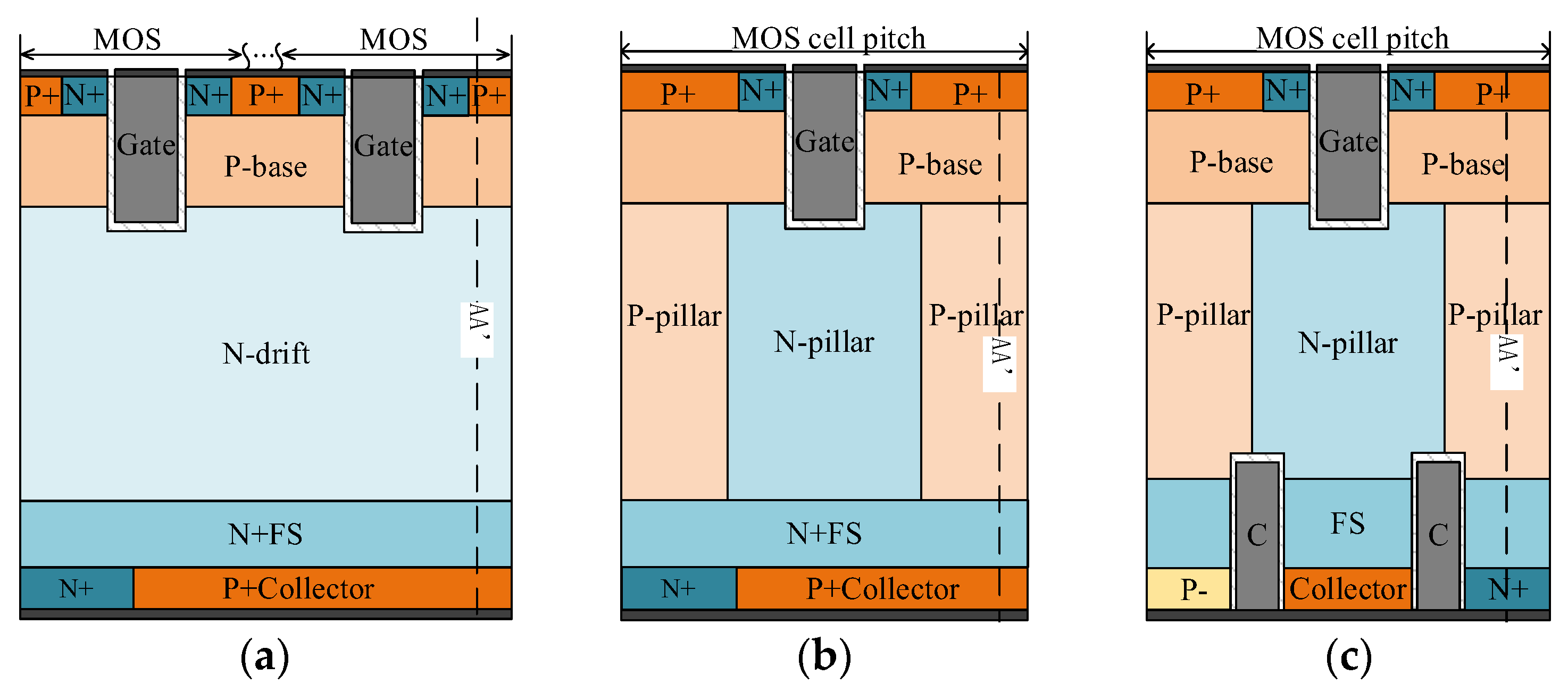
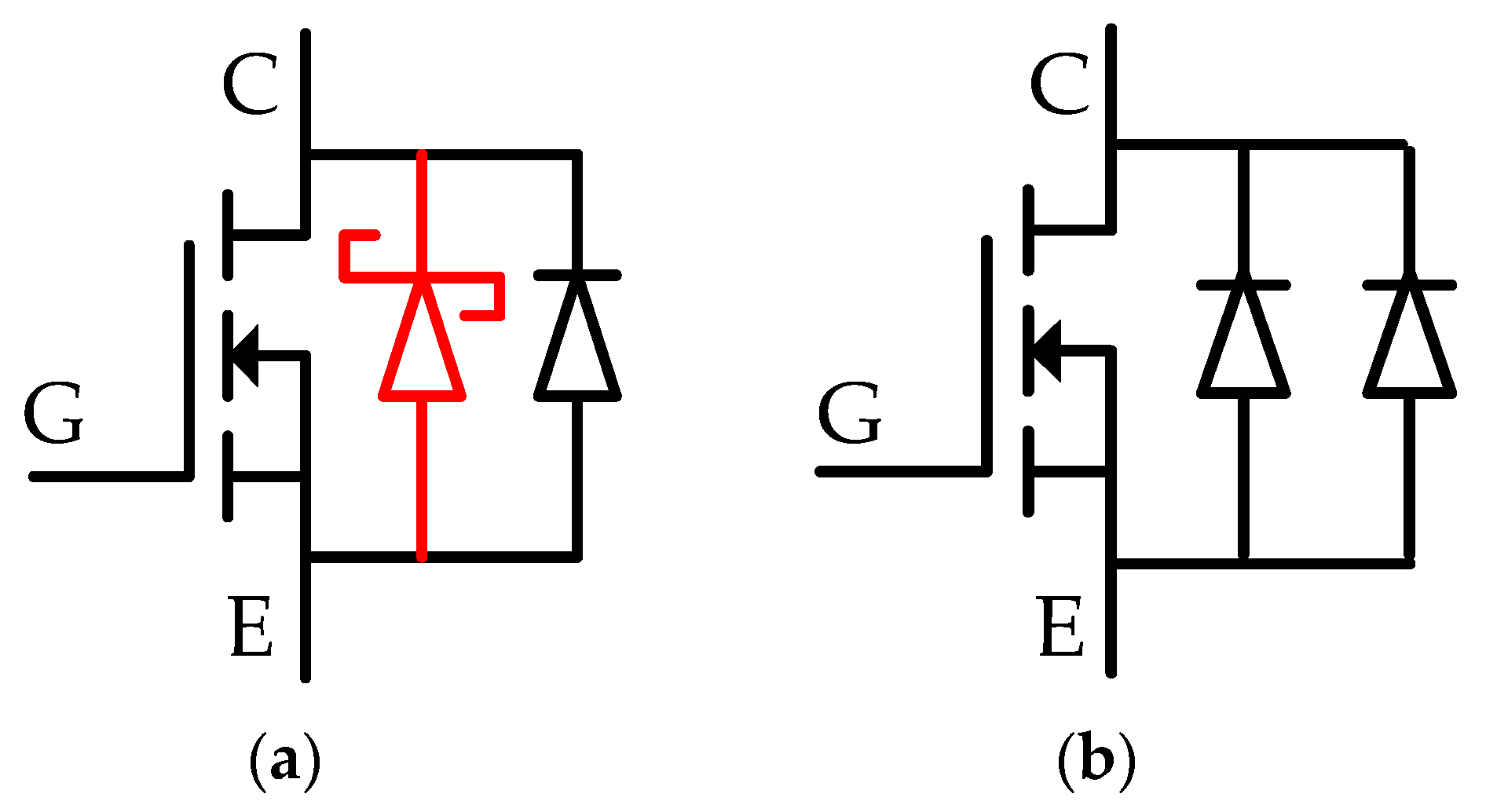
2. Operation Mechanism of Superjunction in RC-IGBTs and the New PSC-SJ-RC-IGBTs
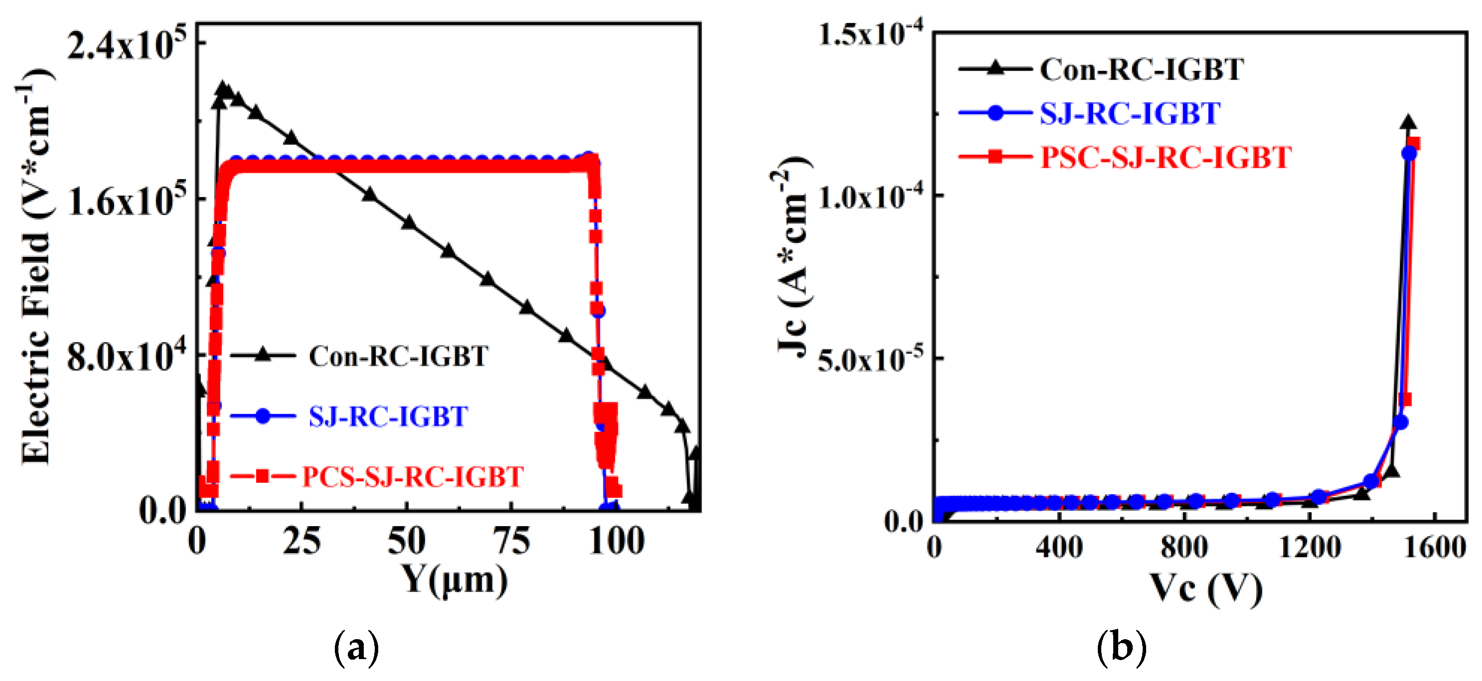
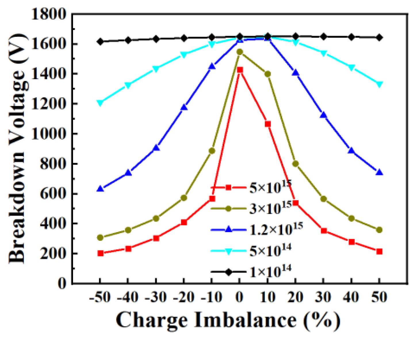
2.1. Breakdown Characteristics
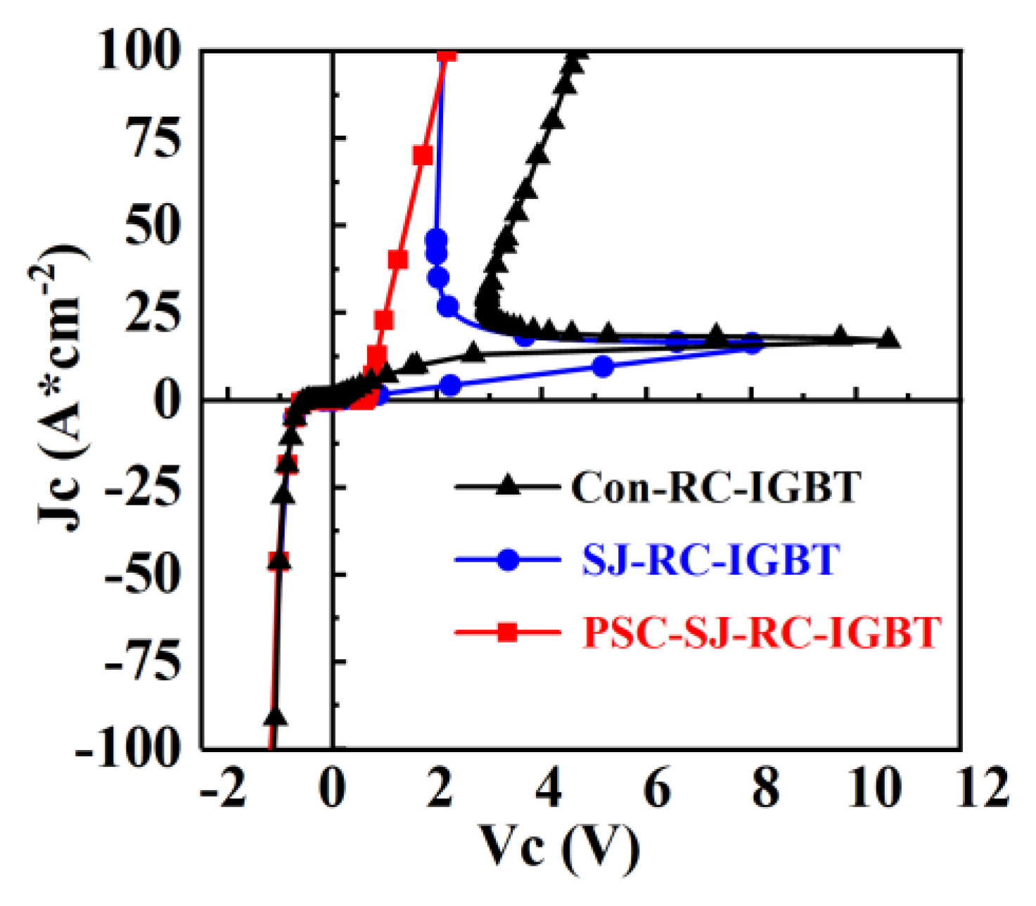
2.2. Forward Conduction Characteristics
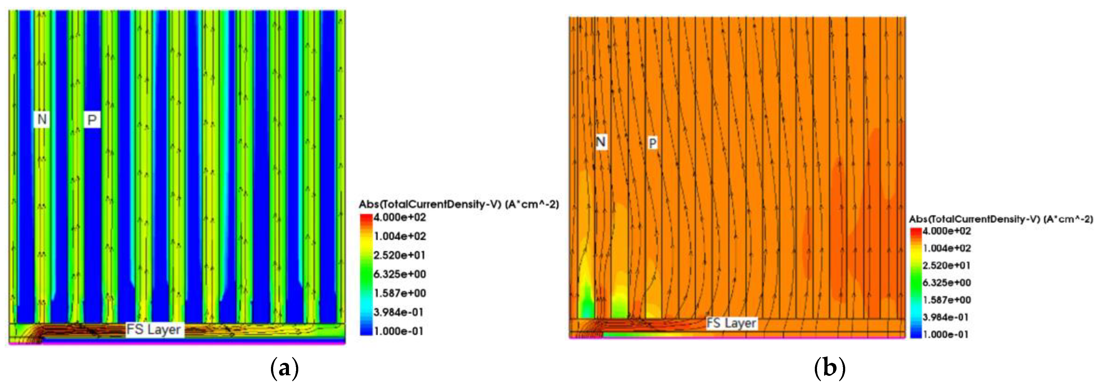
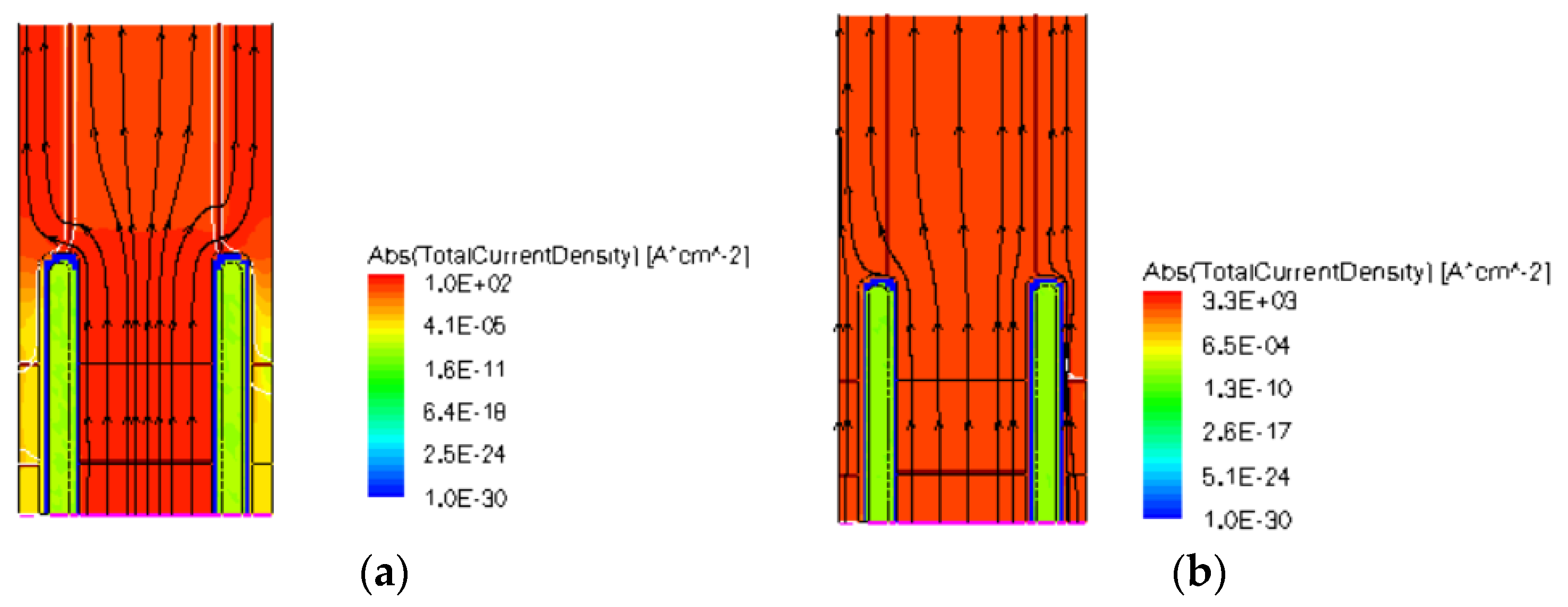
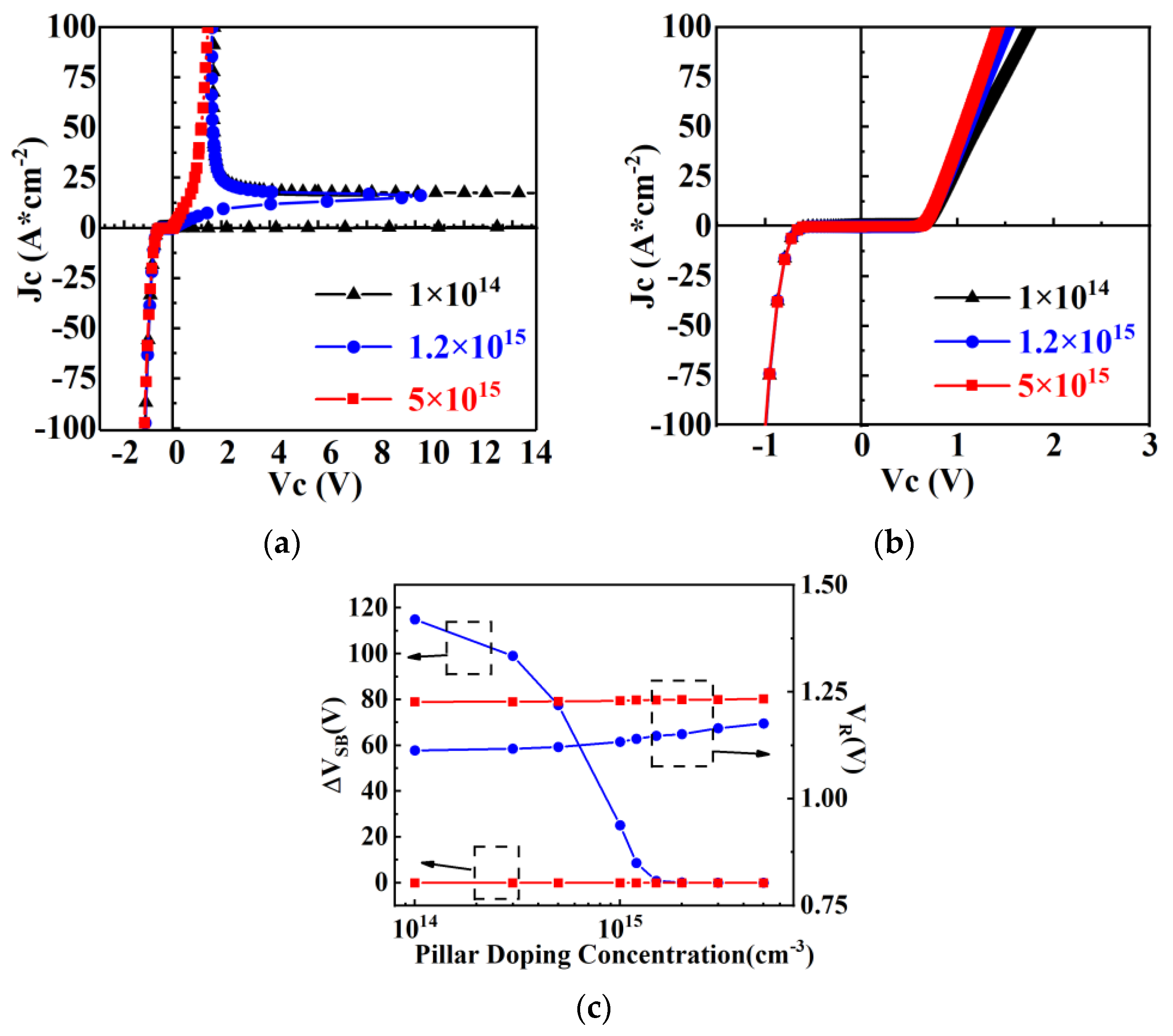
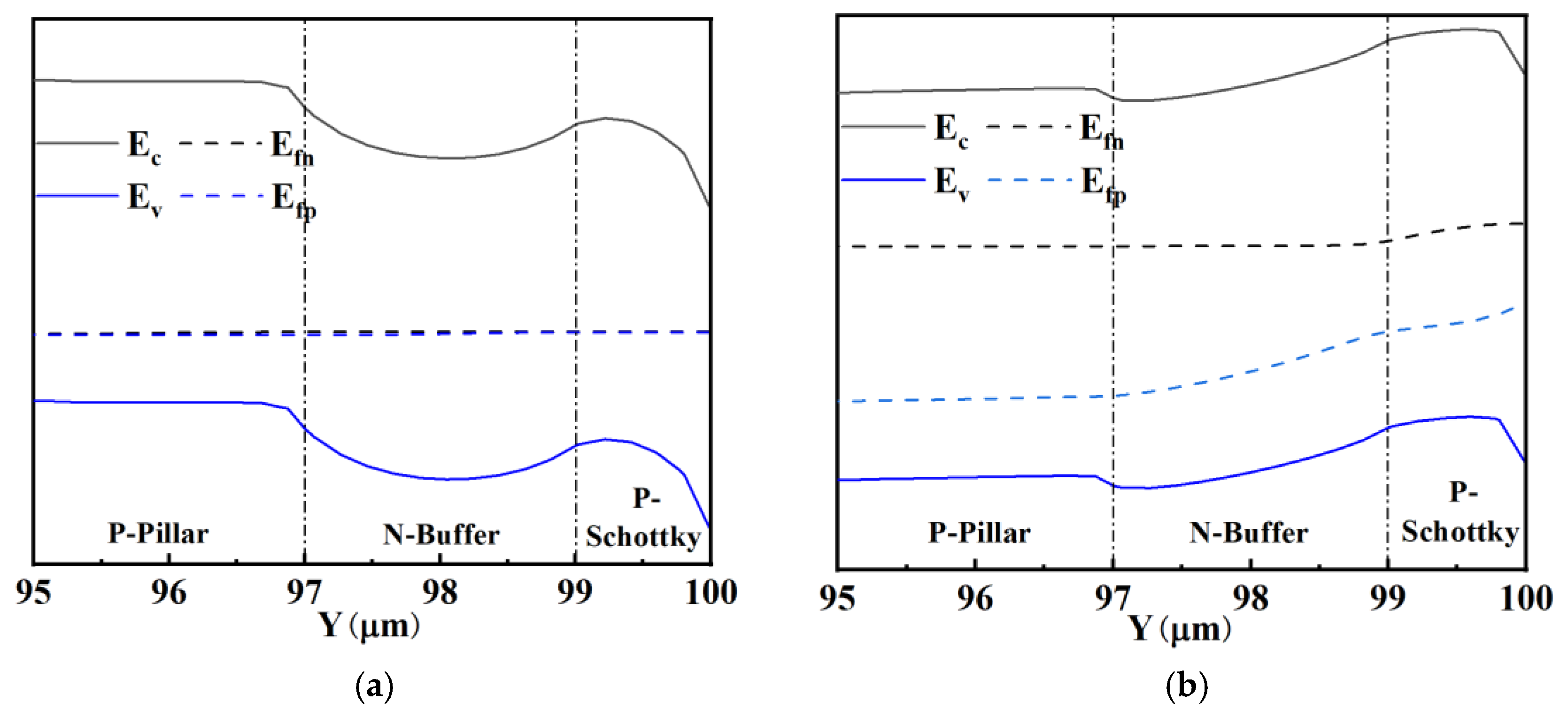
2.2.1. Snapback Mechanism
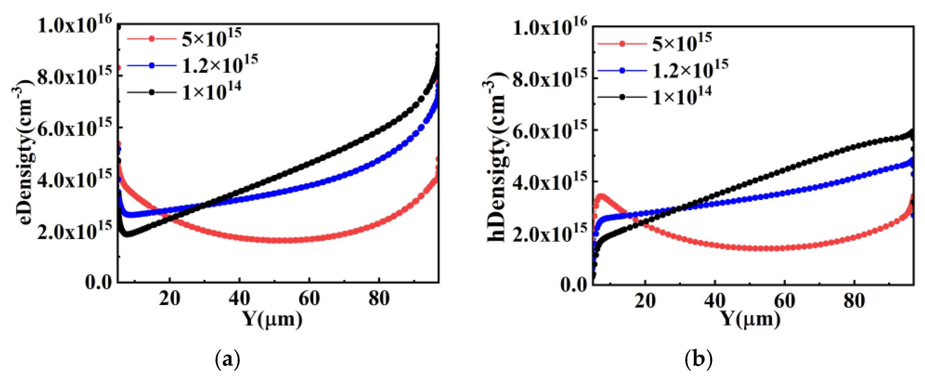
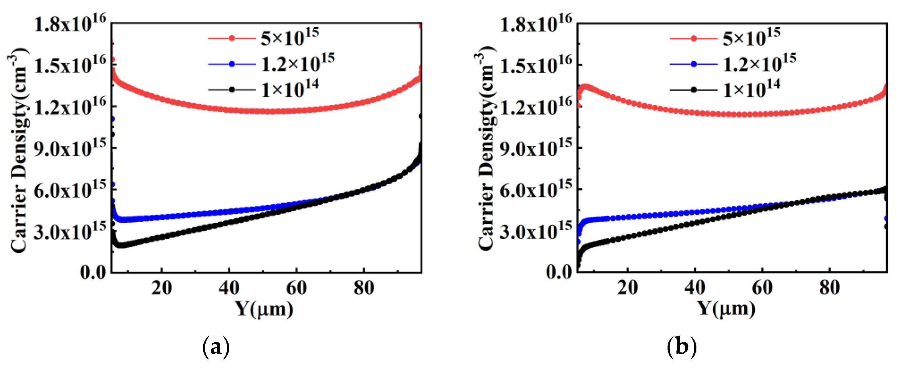
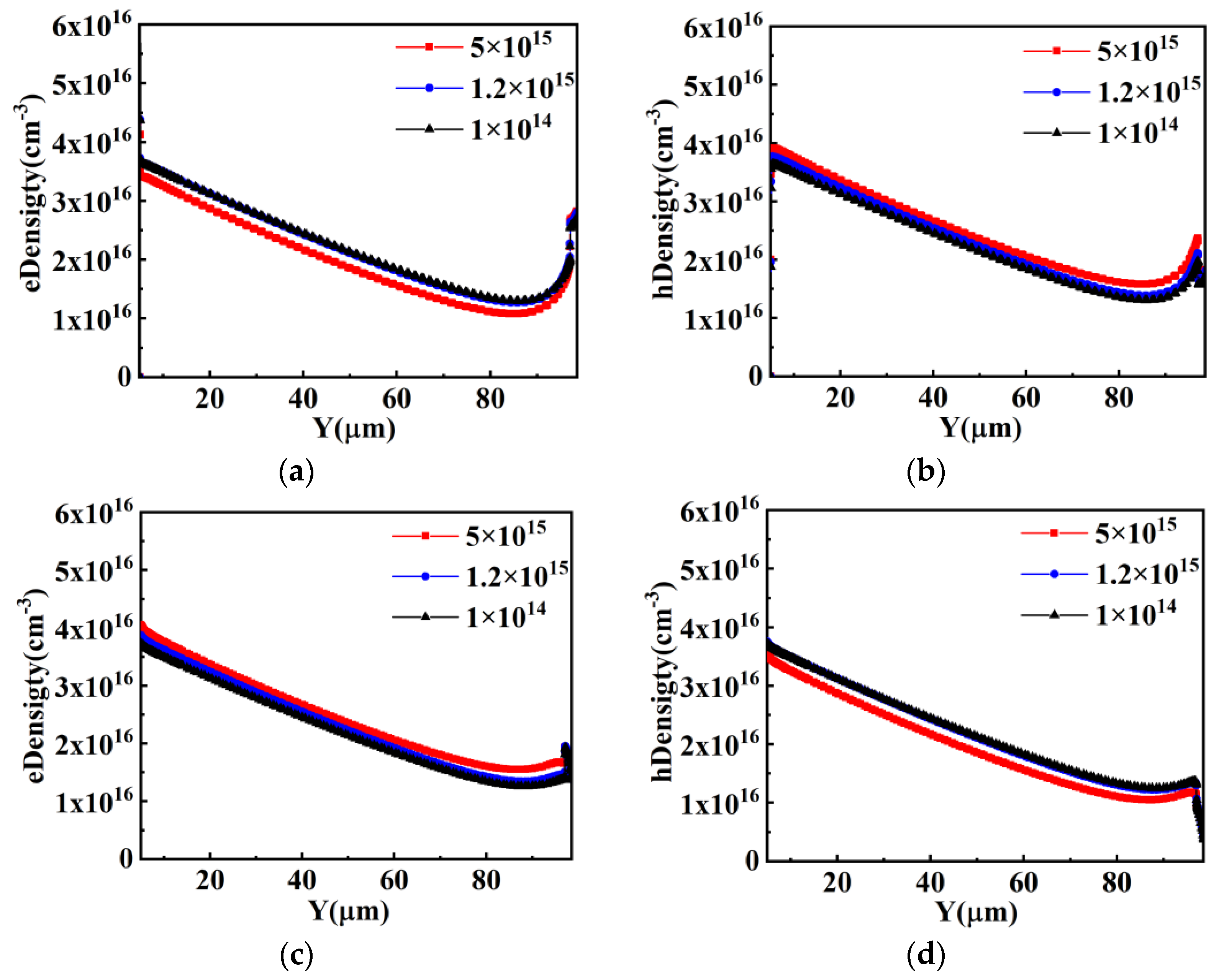
2.2.2. Pillar Doping Influence
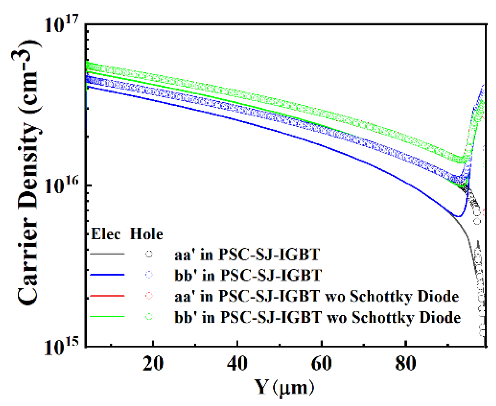
2.3. Reverse Conduction Characteristics
2.4. Switching Characteristics
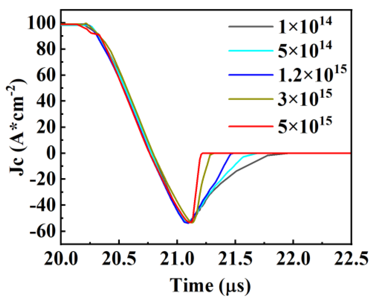
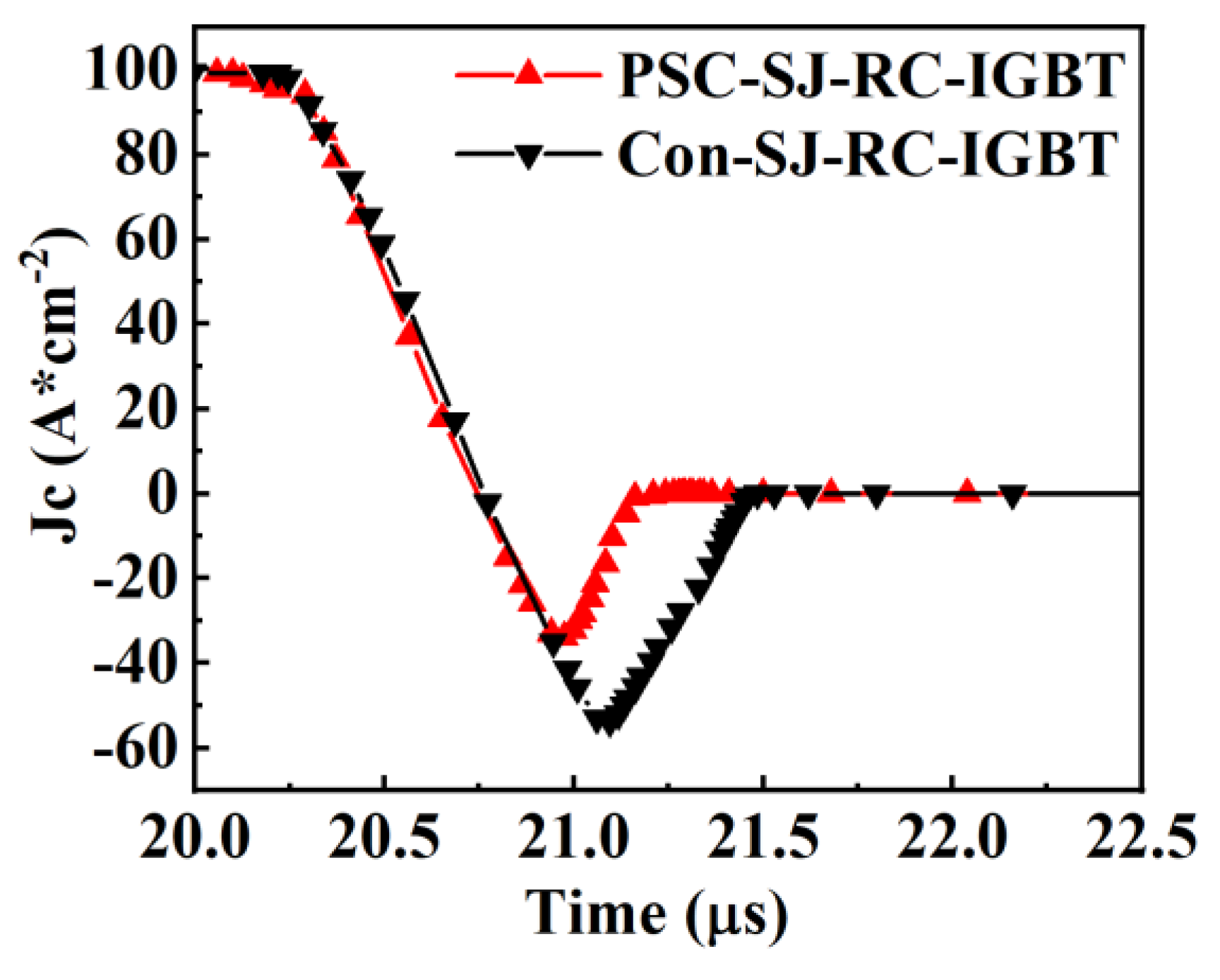
2.4.1. Reverse Recovery
2.4.2. Eoff vs. Vce
3. Results
Author Contributions
Funding
Data Availability Statement
Conflicts of Interest
References
- Ueda, D.; Kitamura, K.; Takagi, H.; Kano, G. A new injection suppression structure for conductivity modulated power MOSFETs. In Proceedings of the 18th Conference on Solid State Devices and Materials, Tokyo, Japan, 1 December 1986. [Google Scholar]
- Laska, T.; Münzer, M.; Pfirsch, F.; Schaeffer, C.; Schmidt, T. The field-stop IGBT (FS IGBT)—A new power device concept with a great improvement potential. In Proceedings of the ISPSD, Toulouse, France, 1 June 2000. [Google Scholar]
- Dewar, S.; Linder, S.; von Arx, C.; Mukhitinov, A.; Debled, G. Soft punch through (SPT)—Setting a new standard in 1200 V IGBT. In Proceedings of the PCIM, Nurnberg, Germany, 6 June 2000. [Google Scholar]
- Kitagawa, M.; Omura, I.; Hasegawa, S.; Inoue, T.; Nakagawa, A. 4500 V injection enhanced insulated gate bipolar transistor (IEGT) operating in a mode similar to a thyristor. In Proceedings of the IEDM Technical Digest, Washington, DC, USA, 5 December 1993. [Google Scholar]
- Takahashi, H.; Haruguchi, H.; Hagino, H.; Yamada, T. Carrier stored trench-gate bipolar transistor—A novel power device for high voltage application. In Proceedings of the ISPSD, Maui, HI, USA, 6 June 1996. [Google Scholar]
- Zhang, F.; Shi, L.; Li, C. Novel Plugged p+ Collector Structure for High-Performance IGBT. IEEE Trans. Plasma Sci. 2006, 34, 1026–1032. [Google Scholar] [CrossRef]
- Luther-King, N.; Sweet, M.; Spulber, O.; Vershinin, K.; De Souza, M.M.; Narayanan, E.S. Striped anode engineering: A concept for fast switching power devices. Solid-State Electron 2002, 46, 903–909. [Google Scholar] [CrossRef]
- Zhang, J.; Zhao, Q.; Luo, J.; Li, Z.; Ren, M.; Li, Z.; Zhang, B. High performance bidirectional IGBT with sandwich super junction structure. In Proceedings of the 2018 IEEE International Conference on Electron Devices and Solid State Circuits (EDSSC), Shenzhen, China, 6 June 2018. [Google Scholar]
- Antoniou, M.; Udrea, F.; Bauer, F. The Superjunction Insulated Gate Bipolar Transistor Optimization and Modeling. IEEE Trans. Electron Devices 2010, 57, 594–600. [Google Scholar] [CrossRef]
- Wang, Z.; Lin, Z.; Zeng, W.; Hu, S.; Zhou, J. Comparison of Short-Circuit Safe Operating Areas Between the Conventional Field-Stop IGBT and the Superjunction Field-Stop IGBT. IEEE J. Electron Devices Soc. 2022, 10, 146–151. [Google Scholar] [CrossRef]
- Chen, W.; Cheng, J.; Huang, H.; Zhang, B.; Chen, X.B. The Oppositely Doped Islands IGBT Achieving Ultralow Turn Off Loss. IEEE Trans. Electron Devices 2019, 66, 3690–3693. [Google Scholar] [CrossRef]
- Wei, J.; Zhang, M.; Chen, K.J. Superjunction IGBT with Conductivity Modulation Actively Controlled by Two Separate Driving Signals. IEEE Trans. Electron Devices 2020, 67, 4335–4339. [Google Scholar] [CrossRef]
- Wang, Z.; Zhang, H.; Kuo, J.B. Turn-OFF Transient Analysis of Superjunction IGBT. IEEE Trans. Electron Devices 2019, 66, 991–998. [Google Scholar] [CrossRef]
- Hsieh, A.P.S.; Camuso, G.; Udrea, F.; Ng, C.; Tang, Y.; Vytla, R.K.; Ranjan, N.; Charles, A. Superjunction IGBT vs. FS IGBT for 200 °C operation. In Proceedings of the 2015 IEEE 27th International Symposium on Power Semiconductor Devices & IC’s (ISPSD), Hong Kong, China, 10 May 2015. [Google Scholar]
- Huang, M.; Gao, B.; Yang, Z.; Lai, L.; Gong, M. A Carrier-Storage-Enhanced Superjunction IGBT with Ultralow Loss and On-State Voltage. IEEE Electron Device Lett. 2018, 39, 264–267. [Google Scholar] [CrossRef]
- Huang, J.; Huang, H.; Chen, X.B. Simulation Study of a Low ON-State Voltage Superjunction IGBT with Self-Biased PMOS. IEEE Trans. Electron Devices 2019, 66, 3242–3246. [Google Scholar] [CrossRef]
- Chen, Y.; Zhang, P.; Hu, X.; Huang, H.Z.; Lai, P.; He, Z.; Chen, Y.; wei Fu, Z.; Liu, C. Study on Electrothermal Characteristics of the Reverse-Conducting IGBT (RC-IGBT). In Proceedings of the 2020 21st International Conference on Electronic Packaging Technology (ICEPT), Guangzhou, China, 12 August 2020. [Google Scholar]
- Yoshida, T.; Takahashi, T.; Suzuki, K.; Tarutani, M. The second-generation 600V RC-IGBT with optimized FWD. In Proceedings of the 2016 28th International Symposium on Power Semiconductor Devices and ICs (ISPSD), Prague, Czech Republic, 12 June 2016. [Google Scholar]
- Feng, H.; Yang, W.; Onozawa, Y.; Yoshimura, T.; Tamenori, A.; Sin, J.K.O. A New Fin p-Body Insulated Gate Bipolar Transistor with Low Miller Capacitance. IEEE Electron Device Lett. 2015, 36, 591–593. [Google Scholar] [CrossRef]
- Xu, X.; Chen, Z. Simulation Study of a Novel Full Turn-On RC-IGBT With Ultralow Energy Loss. IEEE Electron Device Lett. 2019, 40, 757–760. [Google Scholar] [CrossRef]
- Findlay, E.M.; Udrea, F. Reverse-Conducting Insulated Gate Bipolar Transistor: A Review of Current Technologies. IEEE Trans. Electron Devices 2019, 66, 219–231. [Google Scholar] [CrossRef]
- Sun, L.; Duan, B.; Yang, Y. Novel Snapback-Free SOI LIGBT With Shorted Anode and Trench Barriers. IEEE Trans. Electron Devices 2021, 68, 2408–2413. [Google Scholar] [CrossRef]
- Duan, B.; Licheng, S.; Yang, Y. Analysis of the Novel Snapback-Free LIGBT With Fast-Switching and Improved Latch-Up Immunity by TCAD Simulation. IEEE Electron Device Lett. 2019, 40, 63–66. [Google Scholar] [CrossRef]
- Jiang, H.; Zhang, B.; Chen, W.; Li, Z.; Liu, C.; Rao, Z.; Dong, B. A Snapback Suppressed Reverse-Conducting IGBT With a Floating p-Region in Trench Collector. IEEE Electron Device Lett. 2012, 33, 417–419. [Google Scholar] [CrossRef]
- Zhang, J.; Luo, J.; Chen, Z.; Li, Z.; Zhang, B. A Novel Snapback-Free Reverse-Conducting IGBT with Si/SiC Heterojunction. In Proceedings of the 2020 4th IEEE Electron Devices Technology & Manufacturing Conference (EDTM), Penang, Malaysia, 6 April 2020. [Google Scholar]
- Zhu, L.; Chen, X. An Investigation of a Novel Snapback-Free Reverse-Conducting IGBT and With Dual Gates. IEEE Trans. Electron Devices 2012, 59, 3048–3053. [Google Scholar] [CrossRef]
- Deng, G.; Luo, X.; Zhou, K.; He, Q.; Ruan, X.; Liu, Q.; Sun, T.; Zhang, B. A snapback-free RC-IGBT with Alternating N/P buffers. In Proceedings of the 2017 29th International Symposium on Power Semiconductor Devices and IC’s (ISPSD), Sapporo, Japan, 28 May–1 June 2017. [Google Scholar]
- Jiang, H.; Wei, J.; Zhang, B.; Chen, W.; Qiao, M.; Li, Z. Band-to-Band Tunneling Injection Insulated-Gate Bipolar Transistor with a Soft Reverse-Recovery Built-In Diode. IEEE Electron Device Lett. 2012, 33, 1684–1686. [Google Scholar] [CrossRef]
- Antoniou, M.; Udrea, F.; Bauer, F.; Nistor, I. A new way to alleviate the RC IGBT snapback phenomenon: The Super Junction solution. In Proceedings of the 2010 22nd International Symposium on Power Semiconductor Devices & IC’s (ISPSD), Hiroshima, Japan, 6 June 2010. [Google Scholar]
- Zhou, K.; Luo, X.; Huang, L.; Liu, Q.; Sun, T.; Li, Z.; Zhang, B. An Ultralow Loss Superjunction Reverse Blocking Insulated-Gate Bipolar Transistor with Shorted-Collector Trench. IEEE Electron Device Lett. 2016, 37, 1462–1465. [Google Scholar] [CrossRef]
- Yu, J.; Jiang, F.X.C.; Wei, H.; Lin, X. A superjunction snapback-free reverse-conducting insulated gate bipolar transistor with anti-parallel p-i-n diode. In Proceedings of the 2014 12th IEEE International Conference on Solid-State and Integrated Circuit Technology (ICSICT), Guilin, China, 28 October 2014. [Google Scholar]
- Wu, Z.; He, Y.; Liu, D.; Zhang, C.; Ge, X.; Liu, D. Novel Backside Structure for Reverse Conducting Insulated-Gate Bipolar Transistor with Two Different Collector Trench. IEEE Trans. Electron Devices 2022, 69, 4414–4420. [Google Scholar] [CrossRef]
- Zhang, J.P.; Wang, K.; Li, Z.H. Trench isolated SJ RC IGBT filling the gap between SJ MOSFET and SJ IGBT. In Proceedings of the 2019 5th Academic Forum of China IGBT Technology Innovation and Industry Alliance, Zhuzhou, China, 8 December 2009. [Google Scholar]
- Zhou, K.; Huang, L.; Luo, X.; Li, Z.; Li, J.; Dai, G.; Zhang, B. Characterization and performance evaluation of the superjunction RB-IGBT in matrix converter. IEEE Trans. Power Electron 2018, 33, 3286–3301. [Google Scholar] [CrossRef]
- Huang, H.; Chen, X. Optimization of Specific On-Resistance of Balanced Symmetric Superjunction MOSFETs Based on a Better Approximation of Ionization Integral. IEEE Trans. Electron Devices 2012, 59, 2742–2747. [Google Scholar] [CrossRef]
- Yuan, S.; Duan, B.; Cai, H.; Cao, Z.; Yang, Y. Novel LDMOS with assisted deplete-substrate layer consist of super junction under the drain. In Proceedings of the 2017 29th International Symposium on Power Semiconductor Devices and IC’s (ISPSD), Sapporo, Japan, 28 May–1 June 2017. [Google Scholar]
- Li, P.; Guo, J.; Lin, Z.; Hu, S.; Shi, C.; Tang, F. A Low-Reverse-Recovery-Charge Superjunction MOSFET With P-Base and N-Pillar Schottky Contacts. IEEE Trans. Electron Devices 2020, 67, 1693–1698. [Google Scholar] [CrossRef]
- Peng, X.; Liu, Y.; Feng, H.; Huang, L.; Sin, J.K.O. A Fast and Soft Reverse Recovery Diode with a Punch-Through NPN Structure. IEEE Electron Device Lett. 2023, 44, 108–111. [Google Scholar] [CrossRef]
- Zhou, X.; Feng, H.; Sin, J.K.O. A Novel SNOS Gate-Controlled, Normally-Off p-i-n Switch. IEEE Electron Device Lett. 2014, 35, 111–113. [Google Scholar] [CrossRef]
- Lin, Z.; Hu, S.; Yuan, Q.; Zhou, X.; Tang, F. Low reverse recovery charge superjunction MOSFET with a p-type Schottky body diode. IEEE Electron Device Lett. 2017, 38, 1059–1062. [Google Scholar] [CrossRef]


| Parameter | Con-RC-IGBT | SC-SJ-RC-IGBT | PSC-SJ-RC-IGBT |
|---|---|---|---|
| Cell pitch/μm | 50 | 50 | 5 |
| Thickness/μm | 120 | 100 | 100 |
| Drift region Dop/cm−3 | 1 × 10¹⁴ | / | |
| N/P pillars Dop/cm−3 | / | 1 × 10¹⁴~5 × 10¹⁵ | 1 × 10¹⁴~5 × 10¹⁵ |
| N/P pillars width/μm | / | 2.5 | 2.5 |
| FS layer thickness/μm | 5 | 5 | 5 |
| FS layer Dop/cm−3 | 1 × 10¹⁶ | 1 × 10¹⁶ | 1 × 10¹⁶ |
| Collector thickness/μm | 1 | 1 | 1 |
| Collector Dop/cm−3 | 1 × 10¹⁷ | 1 × 10¹⁷ | 1 × 10¹⁷ |
| Gate trench width/μm | 1 | 1 | 1 |
| N collector length/μm | 5 | 5 | 1 |
| Pillar Doping Concentration (cm3) | Cell Pitch to Eliminate Snapback (μm) |
|---|---|
| 1 × 10¹⁴ | 600 |
| 5 × 10¹⁴ | 200 |
| 1.2 × 10¹⁵ | 100 |
| 3 × 10¹⁵ | 50 |
| 5 × 10¹⁵ | 20 |
| Pillar Doping Concentration (cm3) | Con-SJ-RC-IGBT Qrr (μC/cm2) | PSC-SJ-RC-IGBT Qrr (μC/cm2) |
|---|---|---|
| 1 × 10¹⁴ | 24.46 | 12.05 |
| 5 × 10¹⁴ | 22.30 | 11.37 |
| 1.2 × 10¹⁵ | 18.90 | 8.95 |
| 3 × 10¹⁵ | 14.46 | 7.95 |
| 5 × 10¹⁵ | 13.45 | 7.67 |
Disclaimer/Publisher’s Note: The statements, opinions and data contained in all publications are solely those of the individual author(s) and contributor(s) and not of MDPI and/or the editor(s). MDPI and/or the editor(s) disclaim responsibility for any injury to people or property resulting from any ideas, methods, instructions or products referred to in the content. |
© 2023 by the authors. Licensee MDPI, Basel, Switzerland. This article is an open access article distributed under the terms and conditions of the Creative Commons Attribution (CC BY) license (https://creativecommons.org/licenses/by/4.0/).
Share and Cite
Yuan, S.; Li, Y.; Hou, M.; Jiang, X.; Gong, X.; Hao, Y. Analysis of the Operation Mechanism of Superjunction in RC-IGBT and a Novel Snapback-Free Partial Schottky Collector Superjunction RC-IGBT. Micromachines 2024, 15, 73. https://doi.org/10.3390/mi15010073
Yuan S, Li Y, Hou M, Jiang X, Gong X, Hao Y. Analysis of the Operation Mechanism of Superjunction in RC-IGBT and a Novel Snapback-Free Partial Schottky Collector Superjunction RC-IGBT. Micromachines. 2024; 15(1):73. https://doi.org/10.3390/mi15010073
Chicago/Turabian StyleYuan, Song, Yichong Li, Min Hou, Xi Jiang, Xiaowu Gong, and Yue Hao. 2024. "Analysis of the Operation Mechanism of Superjunction in RC-IGBT and a Novel Snapback-Free Partial Schottky Collector Superjunction RC-IGBT" Micromachines 15, no. 1: 73. https://doi.org/10.3390/mi15010073
APA StyleYuan, S., Li, Y., Hou, M., Jiang, X., Gong, X., & Hao, Y. (2024). Analysis of the Operation Mechanism of Superjunction in RC-IGBT and a Novel Snapback-Free Partial Schottky Collector Superjunction RC-IGBT. Micromachines, 15(1), 73. https://doi.org/10.3390/mi15010073