Abstract
Among various polymorphic phases of gallium oxide (Ga2O3), α-phase Ga2O3 has clear advantages such as its heteroepitaxial growth as well as wide bandgap, which is promising for use in power devices. In this work, we demonstrate α-Ga2O3 MOSFETs with hybrid Schottky drain (HSD) contact, comprising both Ohmic and Schottky electrode regions. In comparison with conventional Ohmic drain (OD) contact, a lower on-resistance (Ron) of 2.1 kΩ mm is achieved for variable channel lengths. Physics-based TCAD simulation is performed to validate the turn-on characteristics of the Schottky electrode region and the improved Ron. Electric-field analysis in the off-state is conducted for both the OD and HSD devices. Furthermore, a record breakdown voltage (BV) of 2.8 kV is achieved, which is superior to the 1.7 kV of the compared OD device. Our results show that the proposed HSD contact with a further optimized design can be a promising drain electrode scheme for α-Ga2O3 power MOSFETs.
1. Introduction
Gallium oxide (Ga2O3) semiconductors have been rigorously studied for use in high-performance power devices owing to their ultra-wide bandgap (Eg) and to the high-quality Ga2O3 substrates obtained from a bulk single crystal using melt-growth methods [1,2,3,4]. Interestingly, Ga2O3 crystalizes into five polymorphic phases, and the thermodynamically stable β-Ga2O3 has stood at the center of research. On the other hand, the second most well-known α-Ga2O3 has certain advantages because of its epitaxial compatibility with commercially available, large-size sapphire wafers. Furthermore, the heteroepitaxy of high-quality α-Ga2O3 epilayers on sapphire will allow better thermal conductivity compared with a native substrate [5,6,7,8,9]. It is to be noted that α-Ga2O3 has the highest Eg of ~5.3 eV among Ga2O3 phases and a correspondingly competitive figure of merits. Thus, α-Ga2O3 deserves to be extensively investigated further.
Attributed to its high Eg, α-Ga2O3 has received great interest for ultraviolet (UV) light detectors and specifically deep-UV or UV C-band light (<280 nm) [10,11]. Among various materials with a wide Eg, including aluminum gallium nitride (AlGaN) and zinc oxide (ZnO), α-Ga2O3 is particularly appropriate for large-area processes because of its relatively low growth temperature of about 500 °C. This relatively low temperature of growth or deposition allows not only the use of conventional large-area process methods but also novel Ga2O3 film deposition approaches via thermal oxidation of Ga-based wafers [12,13,14]. These unique advantages of α-Ga2O3 along with large-area film growth techniques make α-Ga2O3 promising for use in high-performance UVC and flame photodetectors.
Power devices based on α-Ga2O3 represent another important application. Indeed, various α-Ga2O3-based device structures have been reported. For example, Schottky barrier diodes using mist-CVD-grown α-Ga2O3 films and α-Ir2O3/α-Ga2O3 hetero p-n junction diodes have been demonstrated [15,16]. Metal-semiconductor field-effect transistors based on a mist-CVD-grown α-Ga2O3 layer on sapphire were also proposed [17]. Jeong et al. reported an α-Ga2O3 MOSFET with a breakdown voltage (BV) of 2.3 kV grown via halide vapor-phase epitaxy (HVPE) [18]. Considering the demonstrated α-Ga2O3 devices’ structures, further enhancement of on-resistance (Ron) and breakdown characteristics can be achieved not only through a vertical structure but also through additional fabrication process steps such as surface passivation and field-plate structures [19,20,21,22,23,24]. Alternatively, the hybrid Schottky–Ohmic drain (HSD) scheme utilizing charge trapping in the Schottky extension region can be considered because of the relatively inferior crystal quality of heteroepitaxial α-Ga2O3 compared to the homoepitaxial Ga2O3 layer [25,26,27,28]. Indeed, the use of HSD on β-Ga2O3 FETs has been reported to alleviate degradation under thermal stress conditions [29].
In this work, for the first time, we propose α-Ga2O3 MOSFETs with HSD electrodes. The heteroepitaxial α-Ga2O3 device layer was grown on a sapphire substrate via HVPE. The HSD is composed of Ti/Al/Ni/Au Ohmic and Ni Schottky electrodes, and both contact regions are analyzed using high-resolution transmission electron microscopy (HR-TEM). The electrical characteristics of the proposed HSD device are compared with a conventional Ohmic drain (OD) device for variable source–drain lengths (LSD). Moreover, physics-based TCAD simulation is performed to elucidate the turn-on characteristics of the proposed HSD device. Electric (E)-field simulation in the off-state is also performed to compare the OD and HSD devices. Finally, the off-state BV of 2.8 kV is measured for the HSD device. The performance is compared with recently reported results.
2. Experimental Section
Heteroepitaxial α-Ga2O3 films were deposited on a 2-inch (0001) sapphire substrate using the HVPE method with GaCl and O2 precursors at a growth temperature of 470 °C. Undoped (~900 nm) and Si-doped α-Ga2O3 (~300 nm) layers were grown for 10 min each, with SiH4 gas supplied as an n-type dopant during the growth of the Si-doped layer. Donor concentration, Hall mobility, and sheet carrier density of the Si-doped α-Ga2O3 epitaxial layer were measured to be 6 × 1017 cm−3, 98.7 cm2/V∙s, and 1.8 × 1013 cm−3, respectively. Surface cleaning was performed for 10 min on each layer using acetone and IPA. The MESA isolation structure was then patterned using BCl3/Ar gas in the appropriate ratio with ICP RIE. The source/drain electrodes were deposited using an e-beam evaporator with a Ti/Al/Ni/Au (25/140/40/100 nm) metal stack and patterned using conventional photolithography and lift-off processes. Rapid thermal annealing was carried out in a N2 ambient at 470 °C for 1 min to improve contact properties. The Schottky drain electrode of Ni (100 nm) is deposited by a DC sputtering system for the HSD device fabrication process. A 20 nm thick HfO2 gate dielectric layer was deposited as the gate oxide using atomic layer deposition at 350 °C with a deposition rate of 1 Å/cycle using Tetrakis (ethylmethy lamino) hafnium precursor and ozone reactant. Finally, the Ni (100 nm) gate electrode was deposited by sputtering, followed by opening contact holes via ICP RIE.
Scanning electron microscopy images and cross-sectional TEM samples were prepared using a dual-beam focused ion beam (FIB-SEM, Helios 460F1). The TEM images and energy dispersive X-ray spectroscopy (EDS) elemental maps were obtained using a JEOL JEM-2100F with a probe Cs corrector. All electrical measurements were conducted using a semiconductor parameter analyzer (Keithley 4200A-SCS) in a dark box. The off-state breakdown measurement was conducted using in-house test equipment composed of a 5 kV power supply (Tektronix model 2290-5), picoammeter (Tektronix model 6485), source-measurement unit (Tektronix model 2440), and protection circuit. Physics-based TCAD (Synopsys, Inc., Mountain View, CA, USA) simulation was performed by elaborately reflecting parameters of the fabricated devices.
3. Results and Discussion
Figure 1a,b show the cross-sectional schematics and a top view of the representative HSD device, respectively. The blue box represents the drain electrode of the OD or HSD. The fabricated α-Ga2O3 MOSFETs have a channel-width (W) = 96 μm with a variable LSD of 20, 28, and 40 µm. The gate length (LG) and source-gate length (LSG) are 2 and 4 µm, respectively. The width of the OD electrode is 96 µm. For the HSD, the Schottky and Ohmic contact regions are designed to be 34 and 62 µm, respectively. The Schottky contact metal is overlaid onto the Ohmic metal by 5 µm. The dashed line shown in Figure 1b indicates the position where TEM images were obtained. Figure 2 compares the TEM and EDS analyses for the Schottky contact (α-Ga2O3/Ni junction) and Ohmic contact (α-Ga2O3/Ti/Al/Ni/Au) regions. Based on the reported band alignment analysis, the Schottky contact between Ni and α-Ga2O3 is predicted. The following equation is used to calculate EC-EF and NC [30]:
where NC, ND, m0, and m* are the effective density of states of the conduction band, electron density of α-Ga2O3, electron mass, and electron effective mass of α-Ga2O3, respectively. Haiying et al. reported that the value of m* for α-Ga2O3 is 0.276 m0 [31]. The calculated NC is 3.65 × 1018 cm−3, and the extracted EC-EF is 0.05 eV. The work function of Ni (ΦNi) is 5.01 eV, and the electron affinity of α-Ga2O3 (χα-Ga2o3) is 3.62 eV [32,33]. Therefore, the barrier height formed in Ni/α-Ga2O3 is calculated to be ΦNi − χα-Ga2o3 − (EC-EF) = 1.34 eV. The interface at the Schottky contact shows a smooth and sharp transition. Although we cannot elaborate it quantitively, the ALD temperature does not have a significant impact on the Schottky contact, as observed from electrical characteristics at a low drain bias. It is reported that interdiffusion is marginal under an annealing temperature of 400 °C and that the Ni content was only 5% in the Ni-Au alloy [34]. The Ohmic contact exhibits a relatively mixed interface due to the formation of a Ti-Al inter-metallic phase, and oxygen vacancies facilitated the Ohmic contact by reducing contact resistance [35].
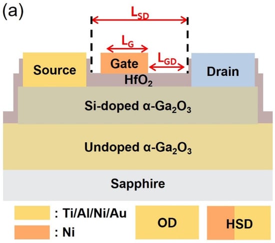
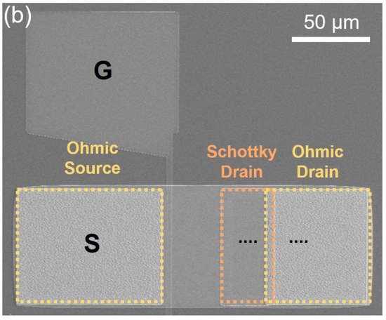
Figure 1.
(a) A cross-sectional schematic and (b) top-view scanning electron microscope image of the fabricated α-Ga2O3 MOSFET with HSD contact. The blue box represents the drain electrode of OD or HSD. Dashed lines (black) show the region of the focused-ion beam milling for HR-TEM analysis.
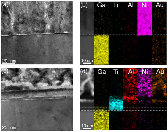
Figure 2.
HR-TEM images and corresponding EDS elemental mapping images of the (a,b) Schottky and (c,d) Ohmic contact regions.
Figure 3a shows transfer characteristics of the representative OD and HSD devices with LSD = 20 μm. The on/off ratios of the devices are 106 at VDS = 10 V. The larger VDS is, the higher the observed off-current is, because the undoped α-Ga2O3 buffer layer is unintentionally an n-doped layer due to the presence of oxygen vacancies. Therefore, even in the off-state, the source–drain current can flow through the buffer layer (i.e., undoped α-Ga2O3), which depends on VDS. Figure 3b presents the output characteristics of the OD and HSD devices. The Ron values of the OD and HSD devices (Ron.OD, Ron.HSD) are extracted to be 2.9 and 2.1 kΩ mm, respectively. The varying slopes at low-VDS regions indicate that the current path forms under the Ohmic and then Schottky regions in turn. In low-drain-bias operation, the HSD affects carrier concentration and increases LGD because the Schottky contact is off. The Schottky and Ohmic contact regions are designed to be 34 and 62 µm, respectively. This significant portion of the Schottky contact region results in a longer LGD (i.e., LSD + the width of Schottky contact) under the low-drain-bias regime because the current flows only via the Ohmic region. Therefore, lower drain currents were observed in the low-drain-bias region of output characteristics. Once the Schottky contact region turns on under high drain bias, however, the current drastically increases because of the current flow via the Schottky contact region because the width of the Schottky contact is larger than the transfer length. Thus, a lower Ron is extracted in comparison with the conventional Ohmic drain contact. Figure 3c compares extracted field-effect mobility (μFE) of the OD and HSD devices for variable LSD at VDS = 1 V and 40 V. The μFE is calculated by μFE = gm · LSD/(W · COX · VDS) in the linear region and μFE = 2 · slope2/(COX · (W/L)) in the saturation region. The oxide capacitance (COX) is calculated to be 712 nF/cm2. The μFE of the HSD device is lower than the OD device at VDS = 1 V because the α-Ga2O3/Ni Schottky junction was not turned on completely, and this can affect the current’s flow toward the drain [29]. In the saturation region, a high VDS of 40 V induces current paths beneath the Schottky region, and thus similar levels of μFE were obtained. Figure 3d also compares extracted Ron.OD and Ron.HSD, and Ron.HSD is lower than Ron.OD regardless of LSD.
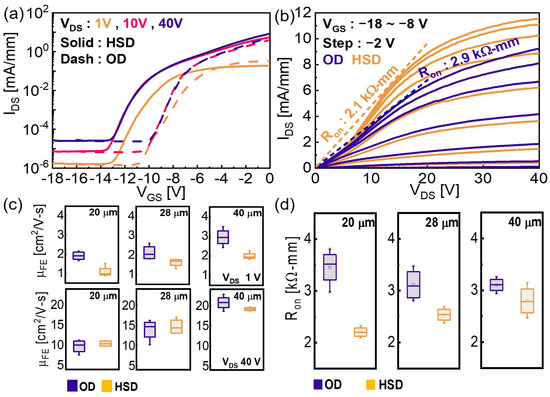
Figure 3.
(a) Transfer and (b) output curves of a representative α-Ga2O3 MOSFET with the OD and HSD contacts. (c) Comparison of extracted μFE for variable LSD = 20, 28, 40 μm from linear (VDS = 1 V) to saturation (VDS = 40 V) region. (d) Comparison of extracted Ron for variable LSD = 20, 28, 40 μm.
Physics-based TCAD simulation was performed to elaborate the turn-on characteristics of the HSD. The simulated OD and HSD devices have same dimensions, including LSD = 40 μm, and the Schottky barrier height of Ga2O3/Ni was calculated based on reported parameters and was set to 1.2 eV [36,37]. Simulation was conducted taking the bias conditions of VGS = 8 V and VDS = 1 and 10 V. Figure 4a,b depict the E-current density distributions in the vicinity of the HSD contact edge at VDS = 1 and 10 V, respectively. Figure 4a shows that the current flow to the Schottky contact region (IHSD.Schottky) is blocked by the depletion of the Schottky region at VDS < VON, and most of the current flows through the Ohmic contact region (IHSD.Ohmic). As shown in Figure 4b, however, IHSD.Schottky takes the form of VDS > VON, indicating two parallel current paths. Figure 4c presents E-current density line profiles along the channel, and clearly shows that IHSD.Schottky formed at a VDS of 10 V. The output curves of the simulated HSD and OD devices are presented in Figure 4d. Until a certain point of VDS, which is 2.5 V in this simulation, the drain current of the HSD device is mostly composed of IHSD.Ohmic. As VDS > 2.5 V, IHSD.Schottky starts to flow and Ron.HSD becomes lower than Ron.OD.
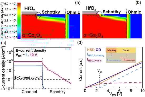
Figure 4.
E-current density distribution of the α-Ga2O3 MOSFET with HSD at (a) VDS = 1 V and (b) 10 V. Dotted lines and circles are cut−line and edge of the Schottky drain, respectively. (c) E-current density line profiles for VDS = 1, 10 V. The E-current cut-off level indicates a minimum value in the color legend. (d) Simulated output curves of HSD and OD. Schematic illustrations of two current components through Schottky and Ohmic contact regions are also presented.
To analyze off-state characteristics, additional simulation of the E-field analysis was conducted for both the HSD and OD devices at VGS = −25 V and VDS = 40 V. Figure 5a compares the simulated E-field distribution below the gate electrode of the HSD and OD device. The OD device exhibits a higher peak E-field at the edge of the gate electrode than the HSD device. Figure 5b,c compare the E-field distributions and corresponding line profiles under the drain region, respectively. The HSD device shows a slightly higher peak E-field at the edge of the drain electrode in comparison with the OD device. The difference at the edge of the gate electrode is significant. Figure 5d,e show line profiles of the E-field under the gate electrode and its corresponding α-Ga2O3/UID interface, respectively. The peak E-field of the HSD device is lower due to the Schottky-contact-induced surface potential change. Additionally, the HSD device exhibits a lower peak E-field at the corresponding region of the α-Ga2O3/UID interface. Considering the undoped α-Ga2O3 buffer layer, which is an unintentionally n-doped layer due to the presence of oxygen vacancies, suppressing the peak E-field at the UID layer might contribute to the breakdown characteristics of the α-Ga2O3 MOSFET [38]. The simulation results foresee enhanced breakdown characteristic from the HSD device, as demonstrated in the following section.
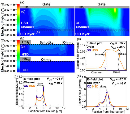
Figure 5.
E-field distribution of the α-Ga2O3 MOSFET with HSD and OD devices near the (a) gate and (b) drain region. (c) Drain E-field line profiles toward lateral axis for OD and HSD. E-field line profiles toward lateral axis for OD and HSD at (d) channel and (e) UID layer.
Figure 6 shows the three-terminal off-state breakdown measurement results for the OD and HSD devices with LSD = 40 μm (gate-to-drain distance is 34 μm). The devices were submerged in a fluorinert liquid (FC-40) to avoid the effects of air-arcing. VGS was set to −16 V to maintain the off-state. The off-state leakage current level was set by our high-current, high-voltage measurement set-up. VDS was swept until the abrupt increase in IDS was observed, which is indicative of a hard breakdown and defined as BV in this work. The BV of the OD and HSD devices is 1.7 and 2.8 kV, respectively. As discussed above, the Schottky contact region with a smooth interface at the edge of drain electrode functions as a drain field-plate, contributing to electric-field distribution and thus an improved BV [26]. The lateral figures of merit (LFOMs) of the OD and HSD devices are calculated as LFOM = BV2/Ron-sp, where Ron-sp is 1.2 and 1 Ω cm2, respectively. The LFOMs of the OD and HSD devices are 2.4 and 7.8 MW/cm2, respectively. The electrical characteristics of the heteroepitaxial Ga2O3 MOSFETs are summarized in Table 1 [18,38,39,40,41,42]. Some parameters are missing because they were not discussed in the published results. A record BV of 2.8 kV is achieved for the HSD device, although the Ron-sp and LFOM are inferior to those in the report by Jeong et al. [18]. Run-to-run epi growth variations are inevitable on account of the growing conditions of HVPE, and the reproducibility needs to be improved. Still, these results fairly demonstrate that the proposed HSD device can be a promising approach to improve BV as well as Ron-sp in comparison with the fabricated OD device. We believe the BV can be further improved by adopting a conventional dielectric passivation layer and a field-plate design.
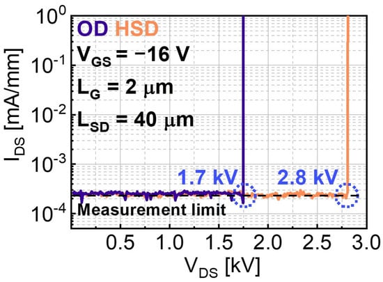
Figure 6.
Three terminal off-state breakdown characteristics of α-Ga2O3 MOSFET with the HSD contact in comparison with the OD device.

Table 1.
Comparison of electrical characteristics of heteroepitaxial Ga2O3 MOSFETs on a sapphire substrate.
4. Conclusions
In summary, we demonstrated HSD contact for heteroepitaxial α-Ga2O3 MOSFETs via HVPE on 2-inch (0001) sapphire wafers. The HSD device, comprising both Ti/Al/Ni/Au Ohmic and Ni Schottky electrode regions, exhibits lower Ron and similar μFE for variable channel lengths of 20, 28, and 40 µm in comparison with conventional OD contact. The Schottky and Ohmic regions were modeled as a parallel electrodes, and turn-on characteristics were elaborated through comprehensive TCAD simulation. Furthermore, off-state simulations for the OD and HSD devices were conducted for comparison and analysis of the E-field distribution, as influenced by the Schottky contact region. The HSD device (LSD = 40 μm) exhibits a record BV of 2.8 kV at a Ron-sp of 1 Ω-cm2, which is superior to the 1.7 kV of the conventional OD device. Our results show that the proposed HSD electrode can be promising with further advanced device structures toward α-Ga2O3 power devices.
Author Contributions
Conceptualization, S.Y.O., Y.J.J. and G.Y.; methodology, S.Y.O., Y.J.J., I.K., J.-H.P., M.J.Y. and D.-W.J.; formal analysis, S.Y.O., Y.J.J. and I.K.; investigation, S.Y.O., Y.J.J., I.K., J.-H.P., D.-W.J. and G.Y.; resources, I.K., D.-W.J. and G.Y.; data curation, S.Y.O. and Y.J.J.; writing—original draft preparation, S.Y.O. and G.Y.; writing—review and editing, S.Y.O. and G.Y.; supervision, G.Y.; project administration, G.Y.; funding acquisition, G.Y. All authors have read and agreed to the published version of the manuscript.
Funding
This research was supported by NRF (2021R1F1A1058006) funded by the Ministry of Education, Republic of Korea, and by KEIT grant (RS-2022-00154729) funded by the Korea Government (MOTIE).
Data Availability Statement
The data presented in this study are available on request from the corresponding author.
Acknowledgments
The EDA tool was supported by the IC Design Education Center, Republic of Korea.
Conflicts of Interest
The authors declare no conflicts of interest. The funders had no role in the design of the study; in the collection, analyses, or interpretation of data; in the writing of the manuscript; or in the decision to publish the results.
References
- Higashiwaki, M.; Sasaki, K.; Murakami, H.; Kumagai, Y.; Koukitu, A.; Kuramata, A.; Masui, T.; Yamakoshi, S. Recent progress in Ga2O3 power devices. Semicond. Sci. Technol. 2016, 31, 034001. [Google Scholar] [CrossRef]
- Pearton, S.J.; Yang, J.; Cary, P.H.; Ren, F.; Kim, J.; Tadjer, M.J.; Mastro, M.A. A review of Ga2O3 materials, processing, and devices. Appl. Phys. Rev. 2018, 5, 011301. [Google Scholar] [CrossRef]
- Kuramata, A.; Koshi, K.; Watanabe, S.; Yamaoka, Y.; Masui, T.; Yamakoshi, S. High-quality β-Ga2O3 single crystals grown by edge-defined film-fed growth. Jpn. J. Appl. Phys. 2016, 55, 1202A2. [Google Scholar] [CrossRef]
- Galazka, Z. Growth of bulk β-Ga2O3 single crystals by the Czochralski method. J. Appl. Phys. 2022, 131, 031103. [Google Scholar] [CrossRef]
- Ahmadi, E.; Oshima, Y. Materials issues and devices of α- and β-Ga2O3. J. Appl. Phys. 2019, 126, 160901. [Google Scholar] [CrossRef]
- Li, X.; Niu, P.; Ning, P.; Jiang, Y. High surface quality heteroepitaxy α-Ga2O3 film on sapphire by mist-CVD technique. Semicond. Sci. Technol. 2023, 38, 075012. [Google Scholar] [CrossRef]
- Kim, K.H.; Ha, M.T.; Kwon, Y.J.; Lee, H.; Jeong, S.M.; Bae, S.Y. Growth of 2-Inch α-Ga2O3 Epilayers via Rear-Flow-Controlled Mist Chemical Vapor Deposition. ECS J. Solid State Sci. Technol. 2019, 8, Q3165. [Google Scholar] [CrossRef]
- McCandless, J.P.; Chang, C.S.; Nomoto, K.; Casamento, J.; Protasenko, V.; Vogt, P.; Rowe, D.; Gann, K.; Ho, S.T.; Li, W.; et al. Thermal stability of epitaxial α-Ga2O3 and (Al,Ga)2O3 layers on m-plane sapphire. Appl. Phys. Lett. 2021, 119, 062102. [Google Scholar] [CrossRef]
- Oshima, Y.; Ahmadi, E. Progress and challenges in the development of ultra-wide bandgap semiconductor α-Ga2O3 toward realizing power device applications. Appl. Phys. Lett. 2022, 121, 260501. [Google Scholar] [CrossRef]
- Kim, S.J.; Yoon, Y.B.; Seo, D.H.; Park, J.H.; Jeon, D.W.; Hwang, W.S.; Shin, M.H. Alpha-phase gallium oxide-based UVC photodetector with high sensitivity and visible blindness. APL Mater. 2023, 11, 061107. [Google Scholar] [CrossRef]
- Almaev, A.; Nikolaev, V.; Kopyev, V.; Shapenkov, S.; Yakovlev, N.; Kushnarev, B.; Pechnikov, A.; Deng, J.; Izaak, T.; Chikiryaka, A.; et al. Solar-Blind Ultraviolet Detectors Based on High-Quality HVPE α-Ga2O3 Films with Giant Responsivity. IEEE Sens. J. 2023, 23, 19245–19255. [Google Scholar] [CrossRef]
- Kim, S.J.; Kim, H.W.; Kim, H.Y.; Jeon, D.W.; Cho, S.B.; Park, J.H. A pre-reaction suppressing strategy for α-Ga2O3 halide vapor pressure epitaxy using asymmetric precursor gas flow. CrystEngComm 2022, 24, 3049–3056. [Google Scholar] [CrossRef]
- Shinohara, D.; Fugita, S. Heteroepitaxy of Corundum-Structured α-Ga2O3 Thin Films on α-Al2O3 Substrates by Ultrasonic Mist Chemical Vapor Deposition. Jpn. J. Appl. Phys. 2008, 47, 7311. [Google Scholar] [CrossRef]
- Solís-Cisneros, H.I.; Vilchis, H.; Hernández-Trejo, R.; Melchor-Tovilla, A.L.; Guillén-Cervantes, Á.; Gutiérrez, C.A.H. Study and characterization of the nanotextured Ga2O3-GaOOH formations synthesized via thermal oxidation of GaAs in ambient air. Semicond. Sci. Technol. 2023, 38, 105004. [Google Scholar] [CrossRef]
- Kan, S.I.; Takemoto, S.; Kaneko, K.; Takahashi, I.; Sugimoto, M.; Shinohe, T.; Fujita, S. Electrical properties of α-Ir2O3/α-Ga2O3 pn heterojunction diode and band alignment of the heterostructure. Appl. Phys. Lett. 2018, 113, 212104. [Google Scholar] [CrossRef]
- Oda, M.; Kikawa, J.; Takatsuka, A.; Tokuda, R.; Sasaki, T.; Kaneko, K.; Fujita, S.; Hitora, T. Vertical Schottky barrier diodes of α-Ga2O3 fabricated by mist epitaxy. In Proceedings of the 2015 73rd Annual Device Research Conference (DRC), Columbus, OH, USA, 21–24 June 2015; pp. 137–138. [Google Scholar]
- Dang, G.T.; Kawaharamura, T.; Furuta, M.; Allen, M.W. Mist-CVD Grown Sn-Doped α-Ga2O3 MESFETs. IEEE Trans. Electron Devices 2015, 62, 3640–3644. [Google Scholar] [CrossRef]
- Jeong, Y.J.; Park, J.H.; Yeom, M.J.; Kang, I.; Yang, J.Y.; Kim, H.Y.; Jeon, D.W.; Yoo, G. Heteroepitaxial α-Ga2O3 MOSFETs with a 2.3 kV breakdown voltage grown by halide vapor-phase epitaxy. Appl. Phys. Express 2022, 15, 074001. [Google Scholar] [CrossRef]
- Farzana, E.; Alema, F.; Ho, W.Y.; Mauze, A.; Itoh, T.; Osinsky, A.; Speck, J.S. Vertical β-Ga2O3 field plate Schottky barrier diode from metal-organic chemical vapor deposition. Appl. Phys. Lett. 2021, 118, 162109. [Google Scholar] [CrossRef]
- Wong, M.H.; Sasaki, K.; Kuramata, A.; Yamakoshi, S.; Higashiwaki, M. Field-Plated Ga2O3 MOSFETs With a Breakdown Voltage of Over 750 V. IEEE Electron Device Lett. 2016, 37, 212–215. [Google Scholar] [CrossRef]
- Xia, X.; Xian, M.; Carey, P.; Fares, C.; Ren, F.; Tadjer, M.; Pearton, S.J.; Tu, T.Q.; Goto, K.; Kuramata, A. Vertical β-Ga2O3 Schottky rectifiers with 750 V reverse breakdown voltage at 600 K. J. Phys. D Appl. Phys. 2021, 54, 305103. [Google Scholar] [CrossRef]
- Sharma, S.; Zeng, K.; Saha, S.; Singisetti, U. Field-Plated Lateral Ga2O3 MOSFETs With Polymer Passivation and 8.03 kV Breakdown Voltage. IEEE Electron Device Lett. 2020, 41, 836–839. [Google Scholar] [CrossRef]
- Lv, Y.; Zhou, X.; Long, S.; Song, X.; Wang, Y.; Liang, S.; He, Z.; Han, T.; Tan, X.; Feng, Z.; et al. Source-Field-Plated Ga2O3 MOSFET With Record Power Figure of Merit of 50.4 MW/cm2. IEEE Electron Device Lett. 2019, 40, 83–86. [Google Scholar] [CrossRef]
- Zeng, K.; Soman, R.; Bian, Z.; Jeong, S.; Chowdhury, S. Vertical Ga2O3 MOSFET With Magnesium Diffused Current Blocking Layer. IEEE Electron Device Lett. 2022, 43, 1527–1530. [Google Scholar] [CrossRef]
- Lian, Y.W.; Lin, Y.S.; Lu, H.C.; Huang, Y.C.; Hsu, S.S.H. AlGaN/GaN HEMTs on Silicon with Hybrid Schottky–Ohmic Drain for High Breakdown Voltage and Low Leakage Current. IEEE Electron Device Lett. 2012, 33, 973–975. [Google Scholar] [CrossRef]
- Lian, Y.W.; Lin, Y.S.; Lu, H.C.; Huang, Y.C.; Hsu, S.S.H. Drain E-Field Manipulation in AlGaN/GaN HEMTs by Schottky Extension Technology. IEEE Trans. Electron Devices 2015, 62, 519–524. [Google Scholar] [CrossRef]
- Tsou, C.W.; Kang, H.C.; Lian, Y.W.; Hsu, S.S.H. AlGaN/GaN HEMTs on Silicon with Hybrid Schottky–Ohmic Drain for RF Applications. IEEE Trans. Electron Devices 2016, 63, 4218–4225. [Google Scholar] [CrossRef]
- Leach, J.H.; Udwary, K.; Rumsey, J.; Dodson, G.; Splawn, H.; Evans, K.R. Halide vapor phase epitaxial growth of β-Ga2O3 and α-Ga2O3 films. APL Mater. 2019, 7, 022504. [Google Scholar] [CrossRef]
- Jeong, Y.J.; Lee, C.H.; Yeom, M.J.; Yang, J.Y.; Yoo, G. A Hybrid Schottky–Ohmic Drain Contact for Thermally Stressed Beta-Gallium Oxide Field-Effect Transistors. Phys. Status Solidi A 2023, 220, 2200596. [Google Scholar] [CrossRef]
- Sasaki, K.; Higashiwaki, M.; Kuramata, A.; Masui, T.; Yamakoshi, S. Ga2O3 Schottky Barrier Diodes Fabricated by Using Single-Crystal β–Ga2O3 (010) Substrates. IEEE Electron Device Lett 2013, 34, 493–495. [Google Scholar] [CrossRef]
- He, H.; Orlando, R.; Blanco, M.A.; Pandey, R.; Amzallag, E.; Baraille, I.; Rerat, M. First-principles study of the structural, electronic, and optical properties of Ga2O3 in its monoclinic and hexagonal phases. Phys. Rev. B 2006, 74, 195123. [Google Scholar] [CrossRef]
- Hinuma, Y.; Gake, T.; Oba, F. Band alignment at surfaces and heterointerfaces of Al2O3, Ga2O3, In2O3, and related group-III oxide polymorphs: A first-principles study. Phys. Rev. Mater. 2019, 3, 084605. [Google Scholar] [CrossRef]
- Haynes, W.M. CRC Handbook of Chemistry and Physics; CRC Press: Boca Raton, FL, USA, 2014. [Google Scholar]
- Massabuau, F.C.P.; Adams, F.; Nicol, D.; Jarman, J.C.; Frentrup, M.; Roberts, J.W.; O’Hanlon, T.J.; Kovacs, A.; Chalker, P.R.; Oliver, R.A. Ni/Au contacts to corundum α-Ga2O3. Jpn. J. of Appl. Phys. 2023, 62, SF1008. [Google Scholar] [CrossRef]
- Chen, J.X.; Li, X.X.; Ma, H.P.; Huang, W.; Ji, Z.G.; Xia, C.; Lu, H.L.; Zhang, D.W. Investigation of the Mechanism for Ohmic Contact Formation in Ti/Al/Ni/Au Contacts to β-Ga2O3 Nanobelt Field-Effect Transistors. ACS Appl. Mater. Interfaces 2019, 11, 32127–32134. [Google Scholar] [CrossRef] [PubMed]
- Mönch, W. On the band-structure lineup at Ga2O3, Gd2O3, and Ga2O3(Gd2O3) heterostructures and Ga2O3 Schottky contacts. J. Mater. Sci. Mater. Electron. 2016, 27, 1444–1448. [Google Scholar] [CrossRef]
- Xu, R.; Lin, N.; Jia, Z.; Liu, Y.; Wang, H.; Yu, Y.; Zhao, X. First principles study of Schottky barriers at Ga2O3(100)/metal interfaces. RSC Adv. 2020, 10, 14746–14752. [Google Scholar] [CrossRef] [PubMed]
- Lu, C.H.; Tarntair, F.G.; Kao, Y.C.; Tumilty, N.; Horng, R.H. Undoped β-Ga2O3 layer thickness effect on performance of MOSFETs grown on sapphire substrate. ACS Appl. Electron. Mater. 2024. [Google Scholar] [CrossRef]
- Park, J.H.; McClintock, R.; Razeghi, M. Ga2O3 metal-oxide-semiconductor field effect transistors on sapphire substrate by MOCVD. Semicond. Sci. Technol. 2019, 34, 08LT01. [Google Scholar] [CrossRef]
- Park, J.H.; McClintock, R.; Jaud, A.; Dehzangi, A.; Razeghi, M. MOCVD grown β-Ga2O3 metal-oxide-semiconductor field effect transistors on sapphire. Appl. Phys. Express 2019, 12, 095503. [Google Scholar] [CrossRef]
- Chen, W.; Luo, H.; Chen, Z.; Pei, Y.; Wang, G.; Lu, X. First demonstration of hetero-epitaxial ε-Ga2O3 MOSFETs by MOCVD and a F-plasma surface doping. Appl. Surf. Sci. 2022, 603, 154440. [Google Scholar] [CrossRef]
- Jeong, Y.J.; Yang, J.Y.; Lee, C.H.; Park, R.; Lee, G.; Chung, R.B.K.; Yoo, G. Fluorine-based plasma treatment for hetero-epitaxial β-Ga2O3 MOSFETs. Appl. Surf. Sci. 2021, 558, 149936. [Google Scholar] [CrossRef]
Disclaimer/Publisher’s Note: The statements, opinions and data contained in all publications are solely those of the individual author(s) and contributor(s) and not of MDPI and/or the editor(s). MDPI and/or the editor(s) disclaim responsibility for any injury to people or property resulting from any ideas, methods, instructions or products referred to in the content. |
© 2024 by the authors. Licensee MDPI, Basel, Switzerland. This article is an open access article distributed under the terms and conditions of the Creative Commons Attribution (CC BY) license (https://creativecommons.org/licenses/by/4.0/).