
Multi-Grid Capacitive Transducers for Measuring the Surface Profile of Silicon Wafers

Abstract
1. Introduction
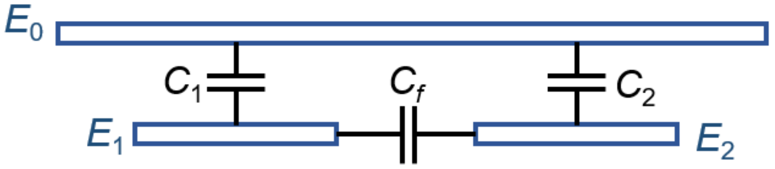
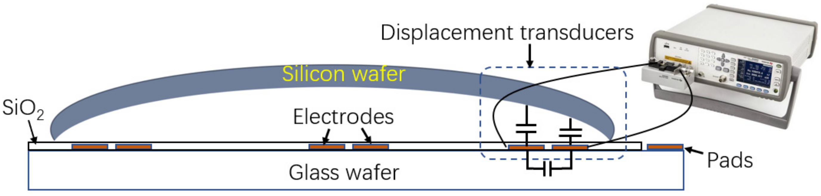
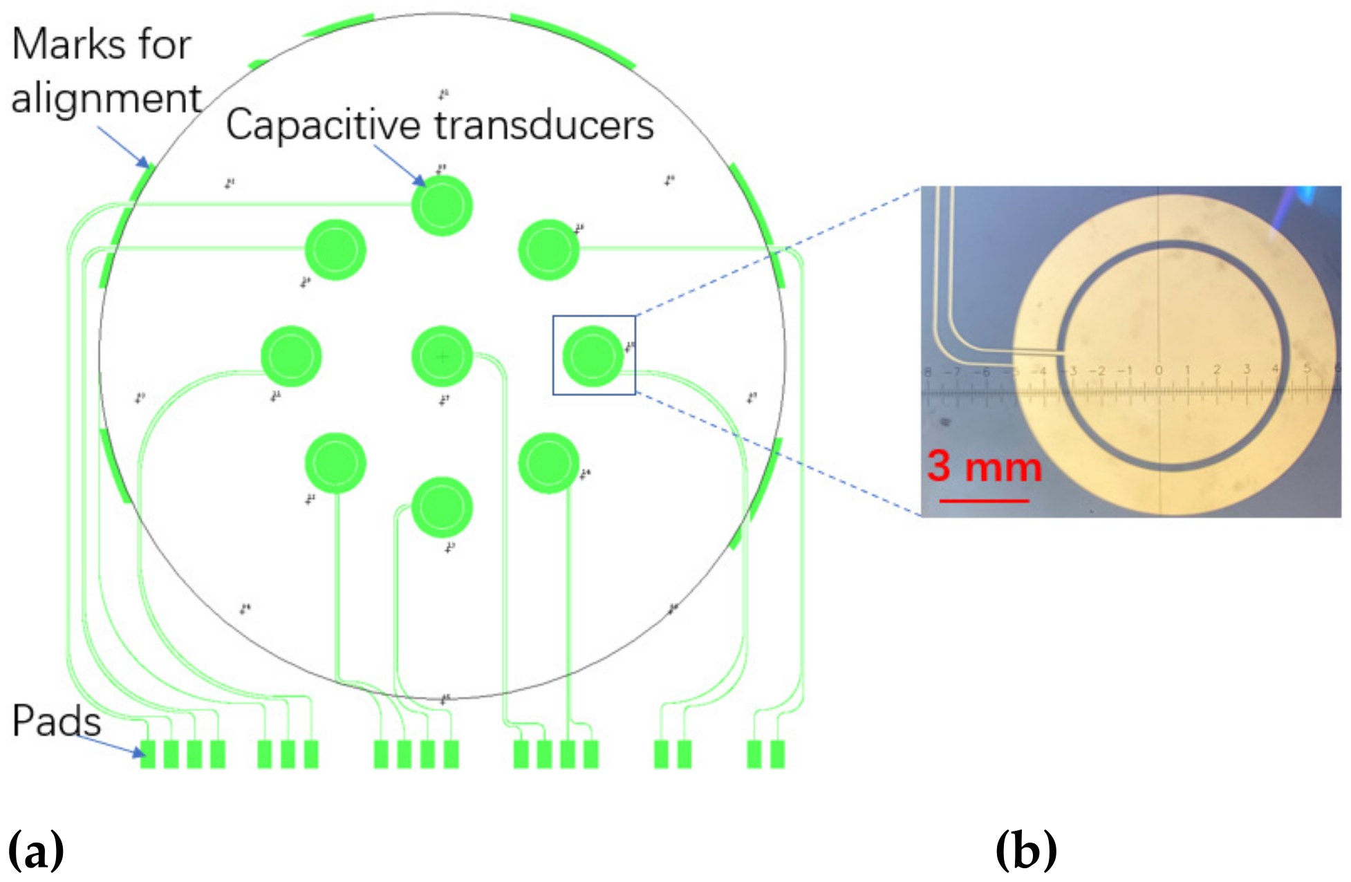
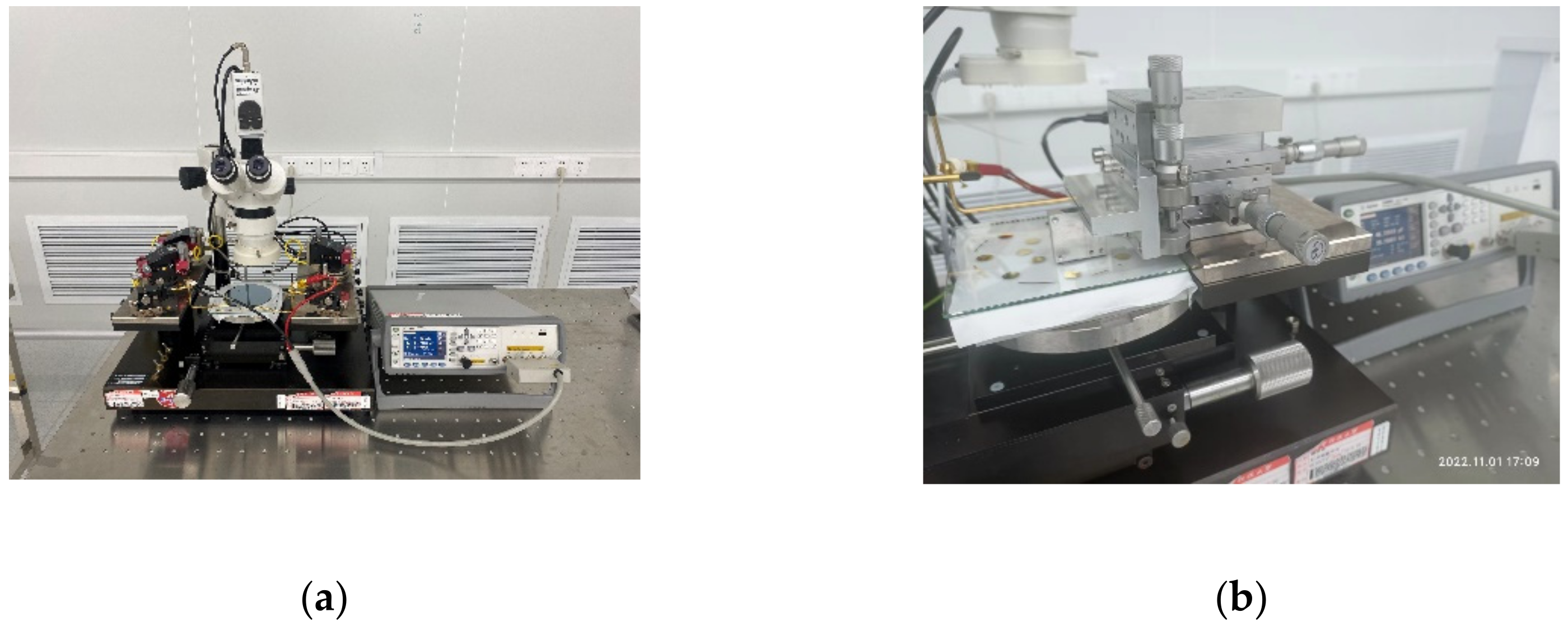
2. Design
3. Results
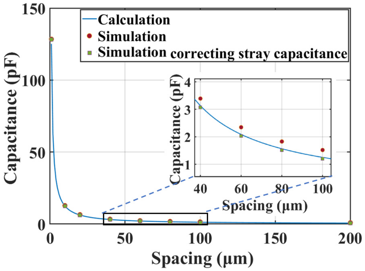
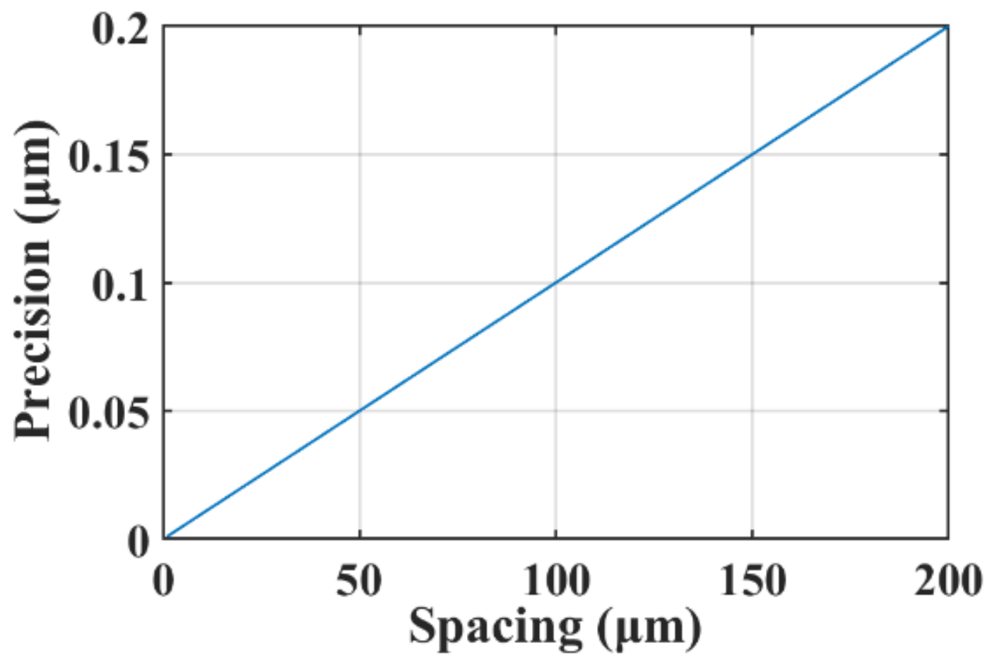
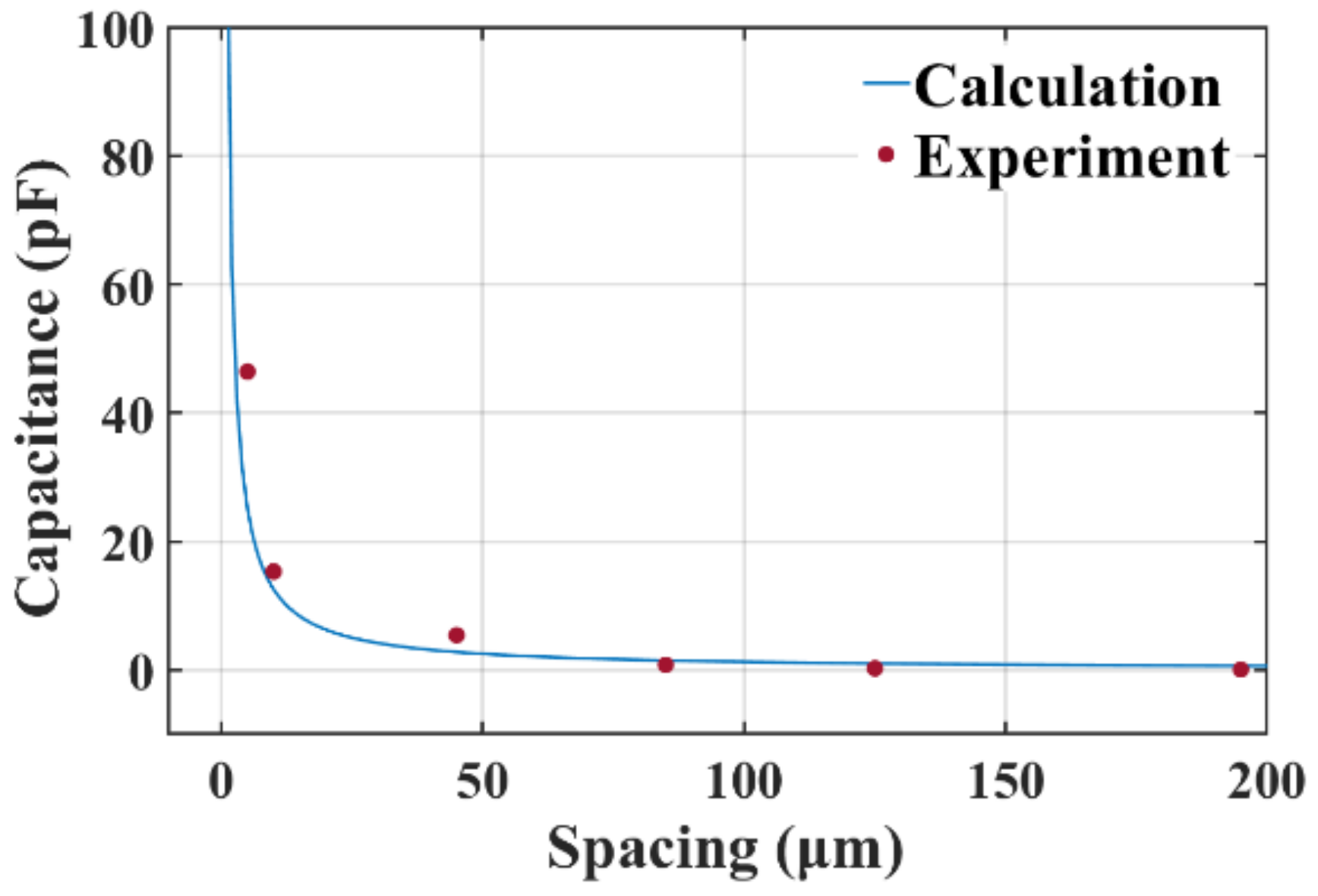
3.1. Calculation, Simulation and Calibration
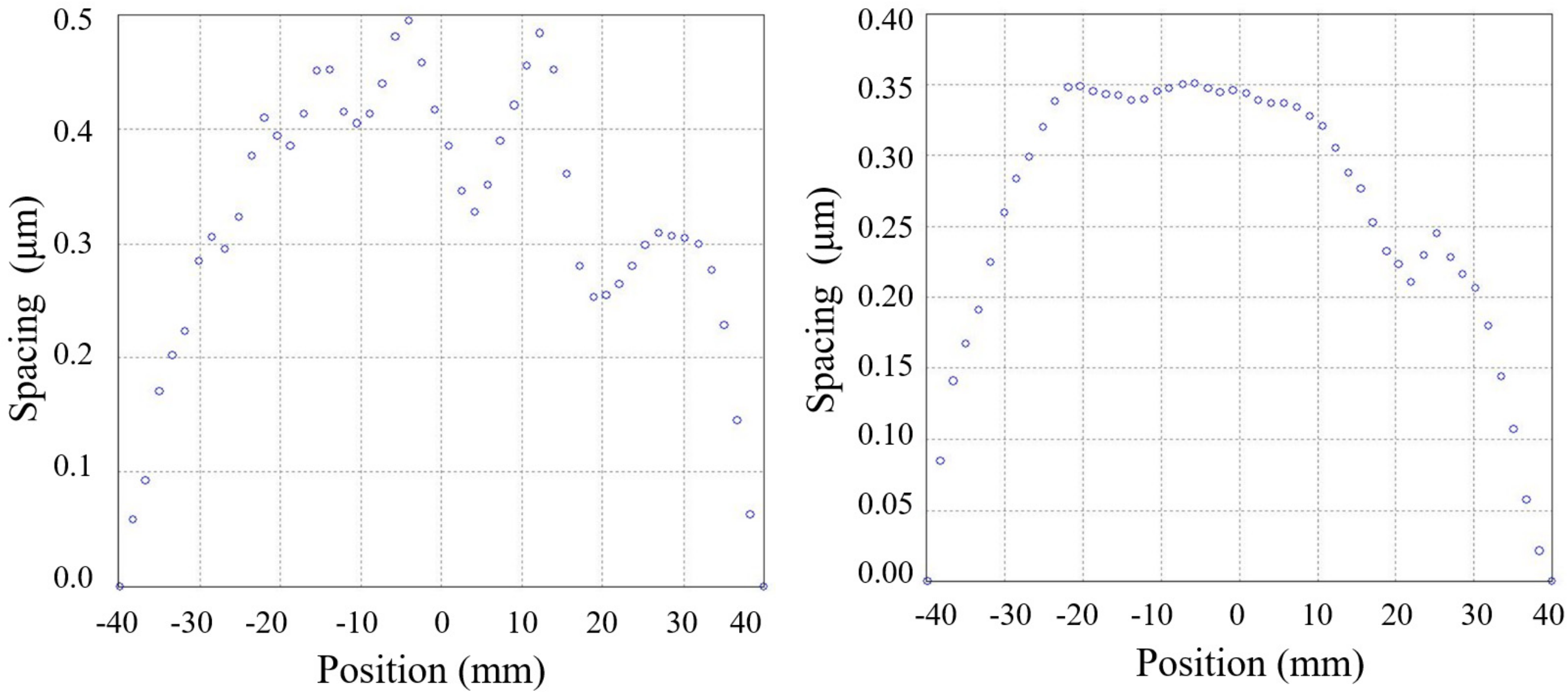
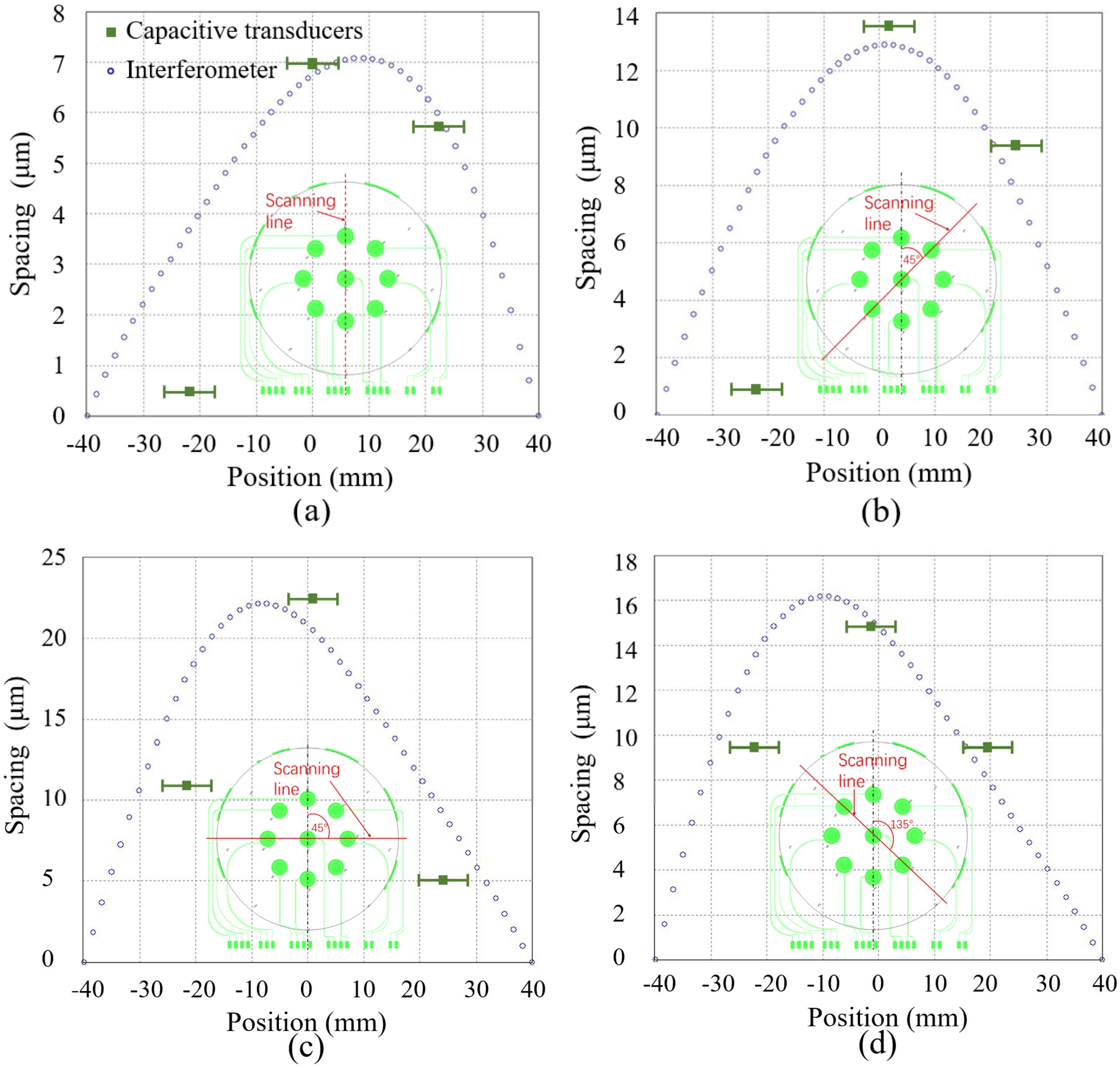
3.2. Surface Profile Measurements
4. Discussion
Author Contributions
Funding
Data Availability Statement
Acknowledgments
Conflicts of Interest
References
- Petersen, K.E. Silicon as a Mechanical Material. Proc. IEEE 1982, 70, 420–457. [Google Scholar] [CrossRef]
- Yeap, K.H.; Nisar, H.; Dakulagi, V. Warpage Reduction for Power Mosfet Wafers. Electrica 2021, 21, 173–179. [Google Scholar] [CrossRef]
- Chu, W.; Rashidi, S.E.E.; Zhang, Y.; Alsmeier, J.; Sega, T. An Analytical Model for Thin Film Pattern-Dependent Asymmetric Wafer Warpage Prediction. In Proceedings of the 2022 IEEE International Memory Workshop, Dresden, Germany, 15–18 May 2022; pp. 2–5. [Google Scholar]
- Cheng, G.; Xu, G.; Gai, W.; Luo, L. Reduce the Wafer Warpage Introduced by Cu in RDL Through Adjusting the Cooling Temperatures. In IEEE 68th Electronic Components and Technology Conference, San Diego, CA, USA, 29 May 2018; pp. 669–674. [Google Scholar] [CrossRef]
- Li, H.; Zhu, C.; Xu, G.; Luo, L. Experimental Identification of Thermal Induced Warpage in Polymer-Metal Composite Films. Microelectron. Reliab. 2016, 62, 141–147. [Google Scholar] [CrossRef]
- Yeon, S.; Park, J.; Lee, H.J. Compensation Method for Die Shift Caused by Flow Drag Force in Wafer-Level Molding Process. Micromachines 2016, 7, 95. [Google Scholar] [CrossRef] [PubMed]
- Yazdi, S.A.F.F.; Garavaglia, M.; Ghisi, A.; Corigliano, A. A New Approach for the Control and Reduction of Warpage and Residual Stresses in Bonded Wafer. Micromachines 2021, 12, 361. [Google Scholar] [CrossRef] [PubMed]
- Marks, M.R.; Hassan, Z.; Cheong, K.Y. Characterization Methods for Ultrathin Wafer and Die Quality: A Review. IEEE Trans. Compon. Packaging Manuf. Technol. 2014, 4, 2042–2057. [Google Scholar] [CrossRef]
- Wu, X.; Tay, A. Influence of Wafer Warpage on Photoresist Film Thickness and Extinction Coefficient Measurements. Metrol. Insp. Process Control. Microlithogr. XXI 2007, 6518, 1446–1453. [Google Scholar] [CrossRef]
- Zhu, C.; Lee, H.; Ye, J.; Xu, G.; Luo, L. A New Designed Trench Structure to Reduce the Wafer Warpage in Wafer Level Packaging Process. In Proceedings of the Electronic Packaging Technology Conference, Chengdu, China, 12–15 August 2014; pp. 606–609. [Google Scholar] [CrossRef]
- Zhu, C.; Ning, W.; Xu, G.; Luo, L. Stress Evolution during Thermal Cycling of Copper/Polyimide Layered Structures. Mater. Sci. Semicond Process. 2014, 27, 819–826. [Google Scholar] [CrossRef]
- Zhu, C.; Ning, W.; Lee, H.; Ye, J.; Xu, G.; Luo, L. Experimental Identification of Warpage Origination during the Wafer Level Packaging Process. In Proceedings-Electronic Components and Technology Conference, Orlando, FL, USA, 27–30 May 2014; pp. 815–820. [Google Scholar] [CrossRef]
- Tay, A.; Ho, W.K.; Hu, N.; Chen, X. Estimation of Wafer Warpage Profile during Thermal Processing in Microlithography. Rev. Sci. Instrum. 2005, 76, 1–8. [Google Scholar] [CrossRef]
- Ku, Y.S.; Shyu, D.M.; Chang, P.Y.; Hsu, W.T. In-Line Metrology of 3D Interconnect Processes. Metrol. Insp. Process. Control. Microlithogr. XXVI 2012, 8324, 1–8. [Google Scholar] [CrossRef]
- Tahara, K.; Matsuoka, H.; Morioka, N.; Kannaka, M. Site Flatness Measurement System with Accuracy of Sub-Nanometer Order for Silicon Wafer. Kobelco Technol. Rev. 2016, 34, 59–64. [Google Scholar]
- Riedel, F.; Gerber, H.A.; Wagner, P. Impact of Filtering on Nanotopography Measurement of 300 Mm Silicon Wafers. Mater. Sci. Semicond. Process. 2002, 5, 465–472. [Google Scholar] [CrossRef]
- Galas, J.; Litwin, D.; Sitarek, S.; Surma, B.; Piatkowski, B.; Miros, A. Interferometric and Confocal Techniques for Testing of Silicon Wafers. In Proceedings of the Optical Micro- and Nanometrology in Microsystems Technology; SPIE, Strasbourg, France, 21 April 2006; pp. 1–8. [Google Scholar]
- Yang, K.H. Optical Imaging Method for Wafer Warpage Measurements. Electrochem. Soc. Ext. Abstr. 1985, 132, 1214. [Google Scholar] [CrossRef]
- Wu, W.; Zheng, P.; Liu, J.; Li, Z.; Fan, J.; Liu, H.; Tu, L. High-Sensitivity Encoder-like Micro Area-Changed Capacitive Transducer for a Nano-g Micro Accelerometer. Sensors 2017, 17, 1–17. [Google Scholar] [CrossRef] [PubMed]


Disclaimer/Publisher’s Note: The statements, opinions and data contained in all publications are solely those of the individual author(s) and contributor(s) and not of MDPI and/or the editor(s). MDPI and/or the editor(s) disclaim responsibility for any injury to people or property resulting from any ideas, methods, instructions or products referred to in the content. |
© 2022 by the authors. Licensee MDPI, Basel, Switzerland. This article is an open access article distributed under the terms and conditions of the Creative Commons Attribution (CC BY) license (https://creativecommons.org/licenses/by/4.0/).
Share and Cite
Zheng, P.; Cai, B.; Zhu, T.; Yu, L.; Wu, W.; Tu, L. Multi-Grid Capacitive Transducers for Measuring the Surface Profile of Silicon Wafers. Micromachines 2023, 14, 122. https://doi.org/10.3390/mi14010122
Zheng P, Cai B, Zhu T, Yu L, Wu W, Tu L. Multi-Grid Capacitive Transducers for Measuring the Surface Profile of Silicon Wafers. Micromachines. 2023; 14(1):122. https://doi.org/10.3390/mi14010122
Chicago/Turabian StyleZheng, Panpan, Bingyang Cai, Tao Zhu, Li Yu, Wenjie Wu, and Liangcheng Tu. 2023. "Multi-Grid Capacitive Transducers for Measuring the Surface Profile of Silicon Wafers" Micromachines 14, no. 1: 122. https://doi.org/10.3390/mi14010122
APA StyleZheng, P., Cai, B., Zhu, T., Yu, L., Wu, W., & Tu, L. (2023). Multi-Grid Capacitive Transducers for Measuring the Surface Profile of Silicon Wafers. Micromachines, 14(1), 122. https://doi.org/10.3390/mi14010122