
Towards Robust Thermal MEMS: Demonstration of a Novel Approach for Solid Thermal Isolation by Substrate-Level Integrated Porous Microstructures


Abstract
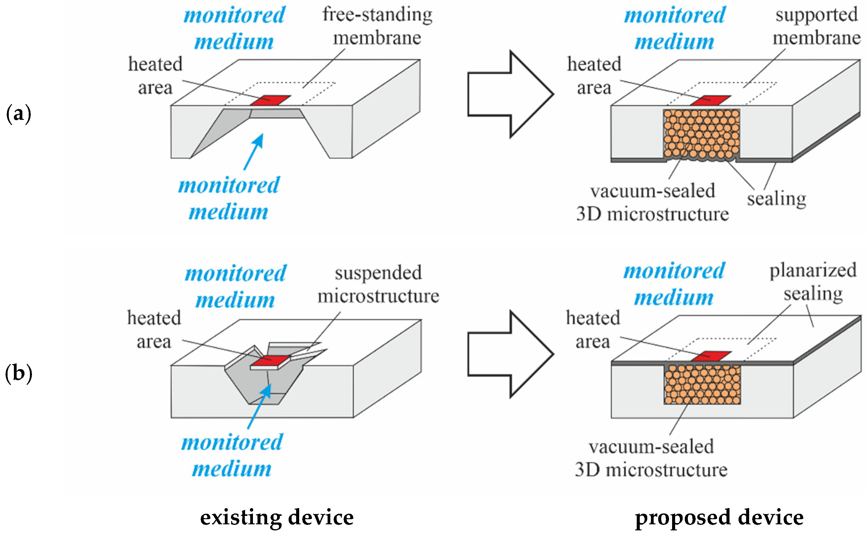
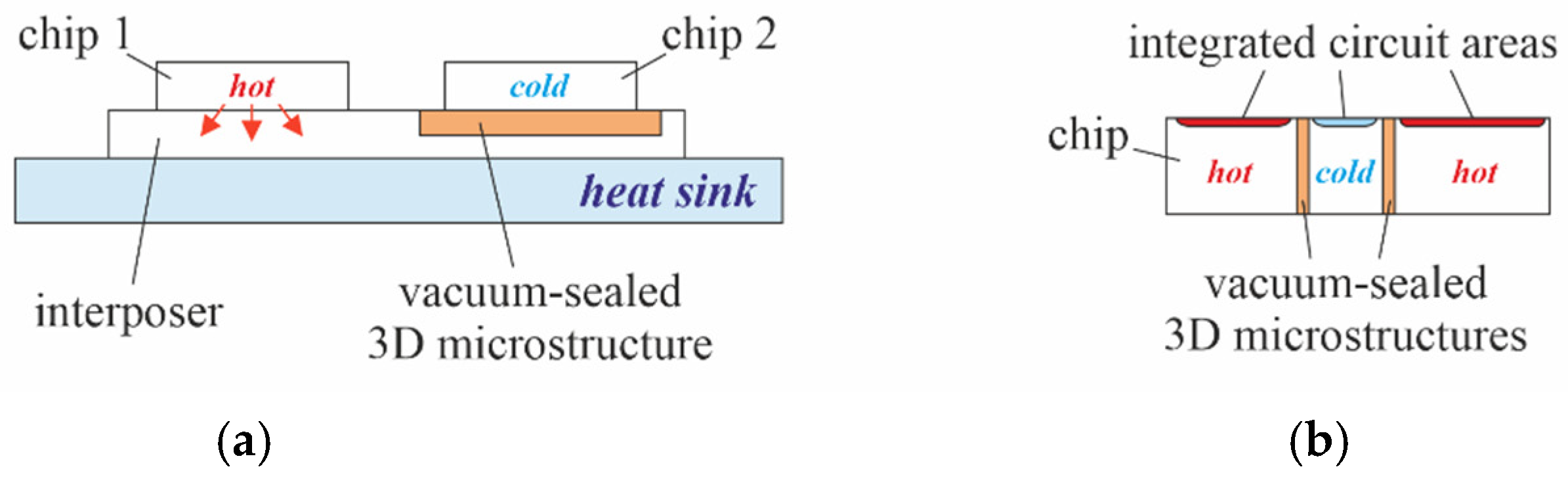
:1. Introduction
2. Materials and Methods
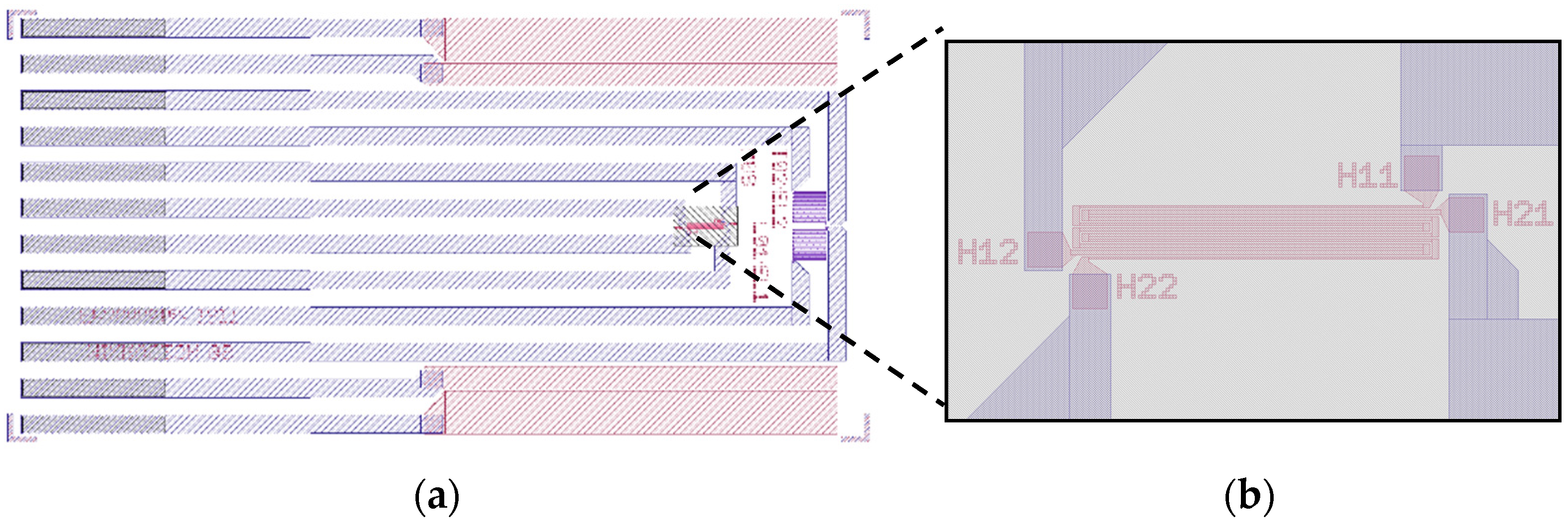
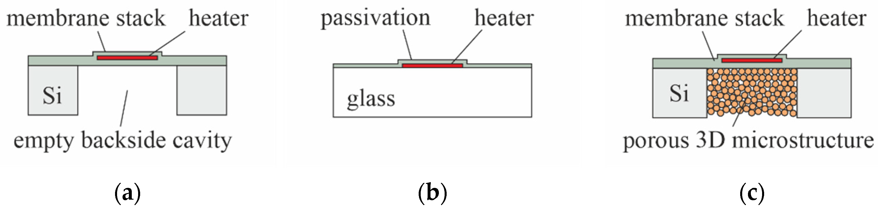
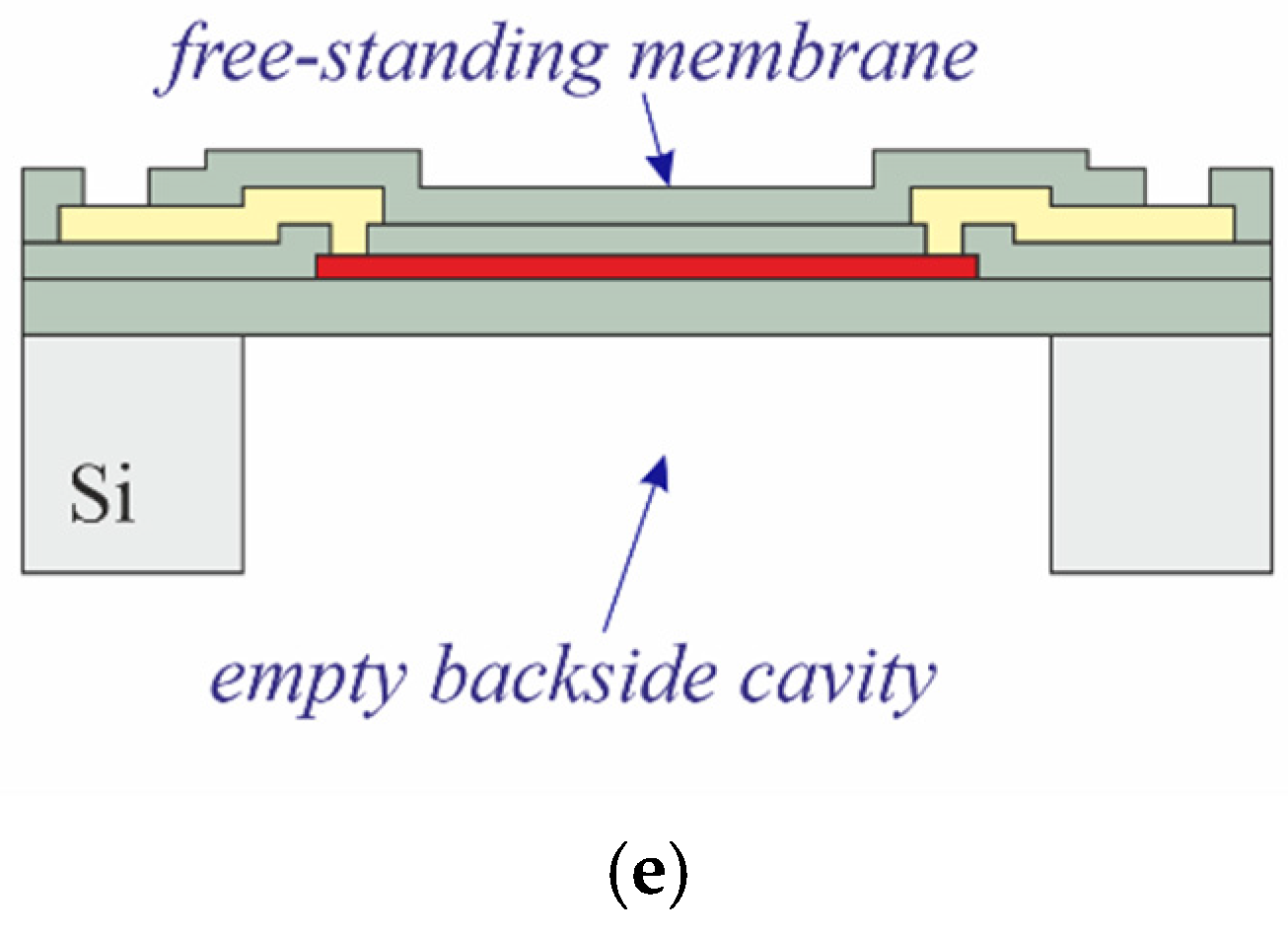
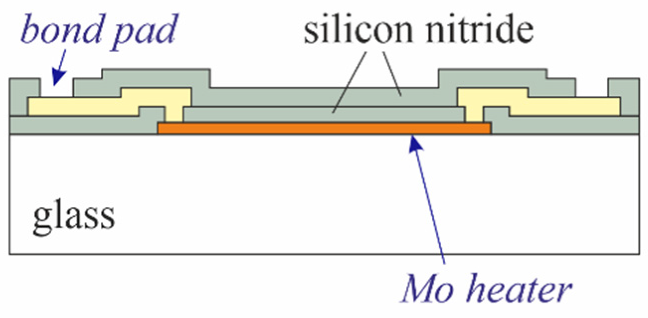
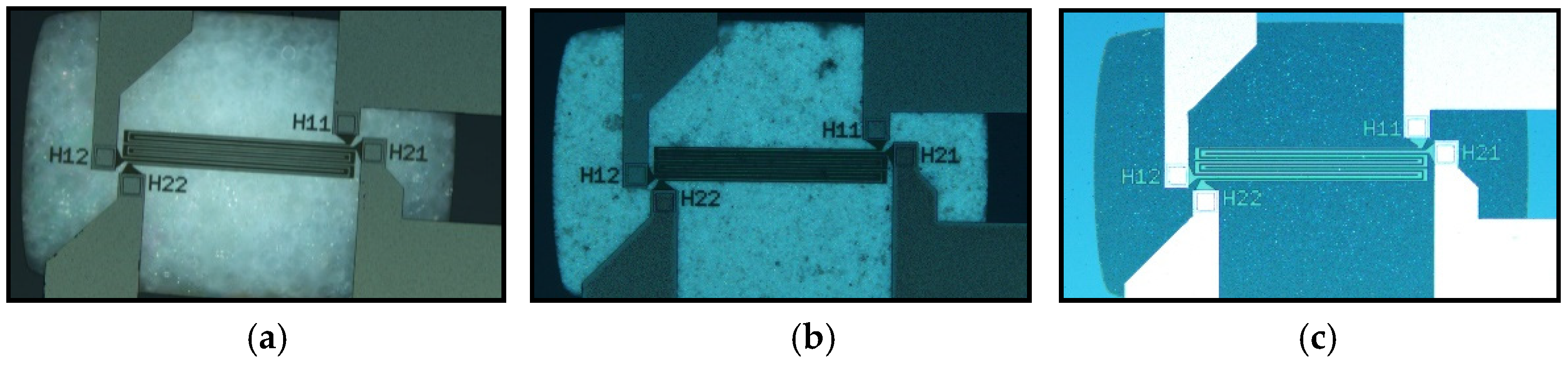
2.1. Sensor Layout
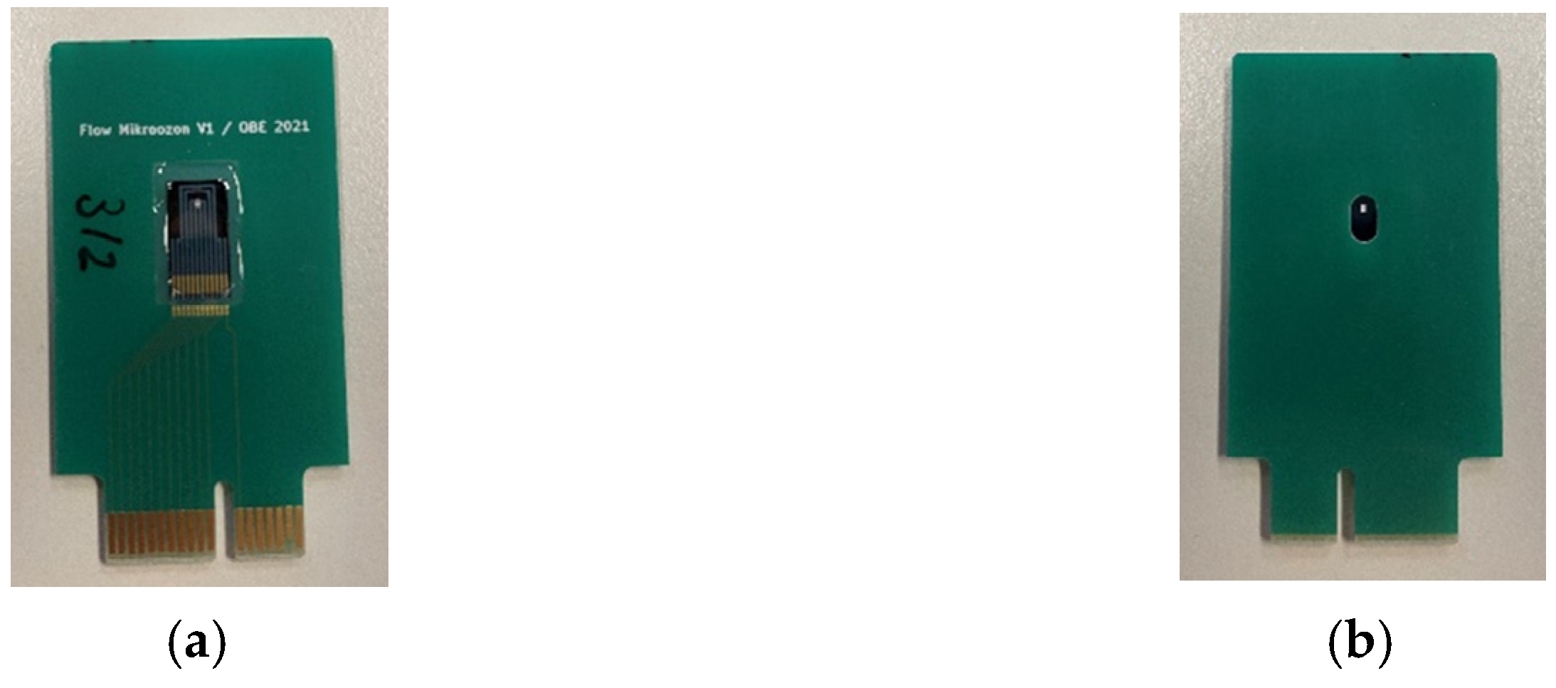
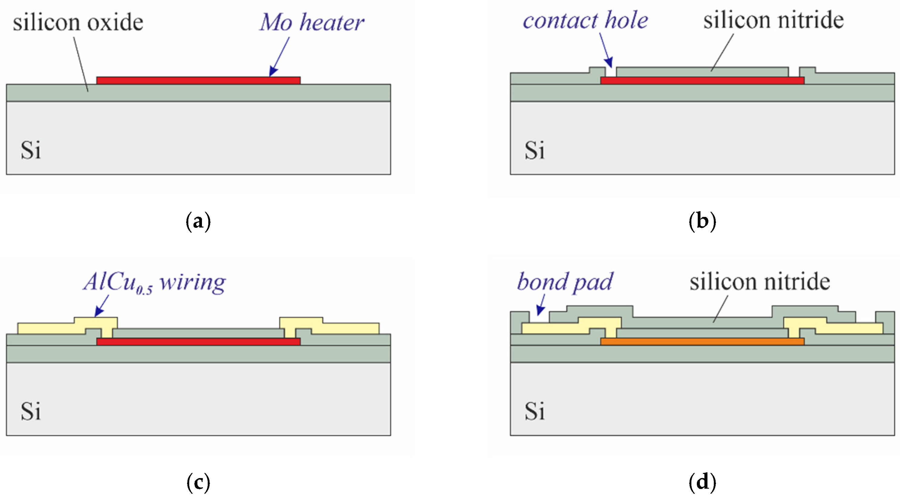
2.2. Sensor Fabrication
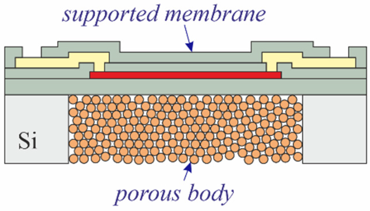
2.3. PowderMEMS Modification
2.4. Measurement Setup
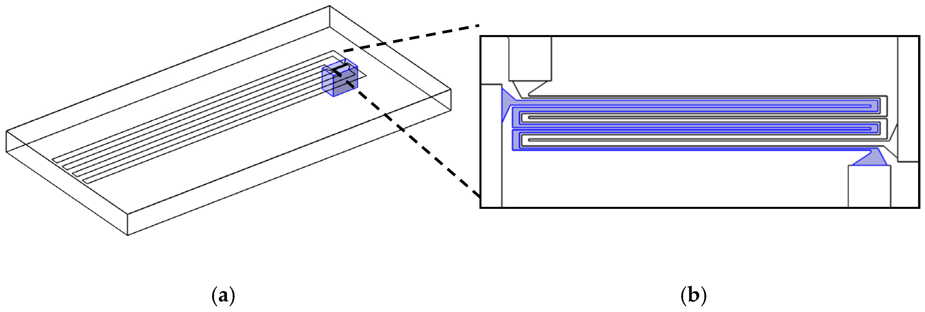
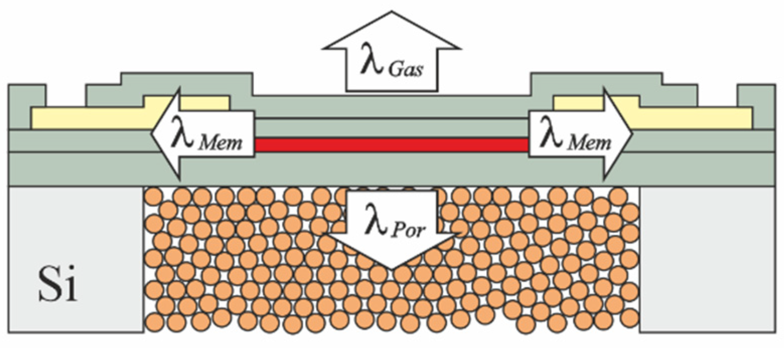
2.5. Measurement Principle and Simulation Model
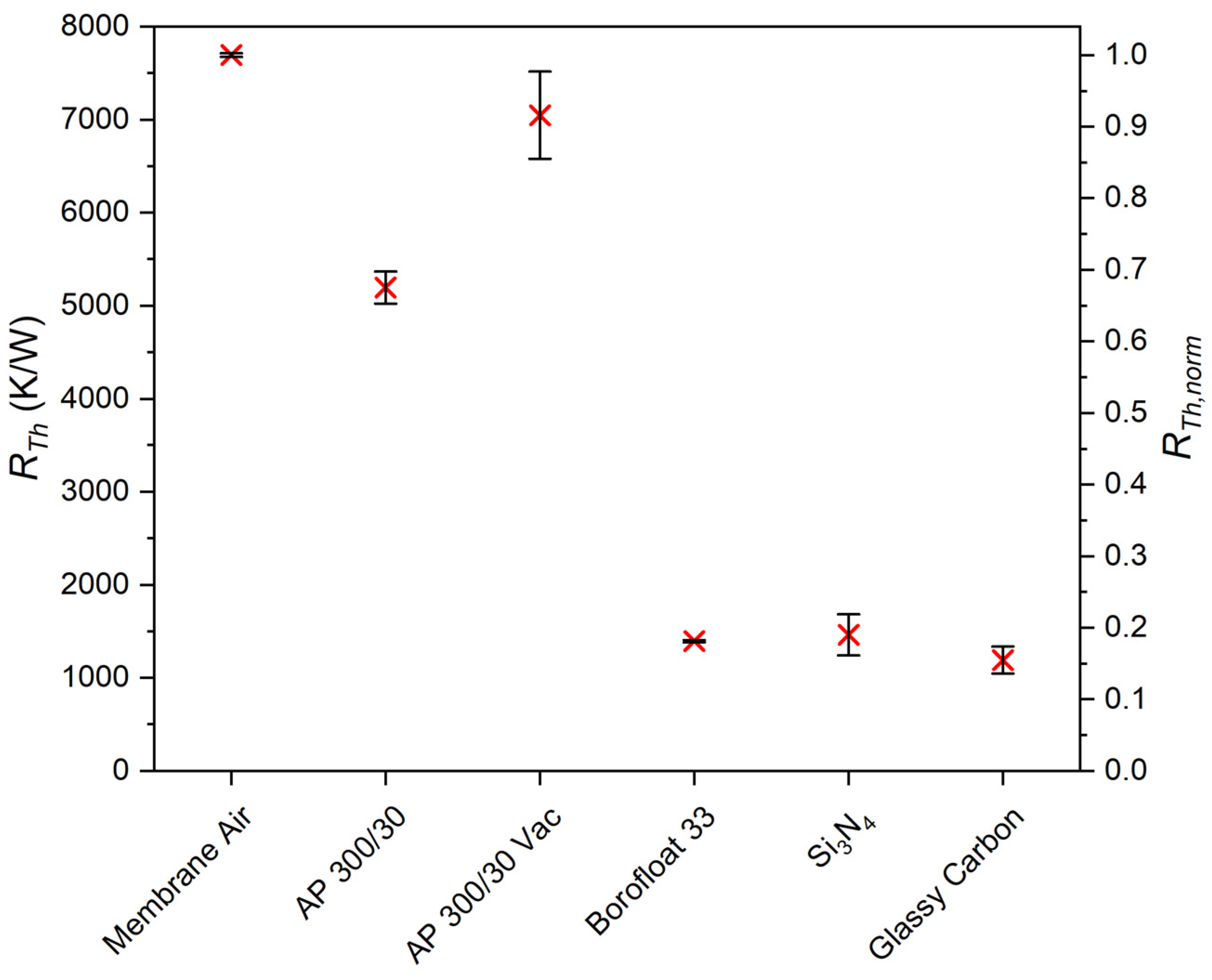
3. Results
3.1. Measurement of the TCR
3.2. PowderMEMS Microsctructures
3.3. Thermal Conductivity of the PowderMEMS Microstructure
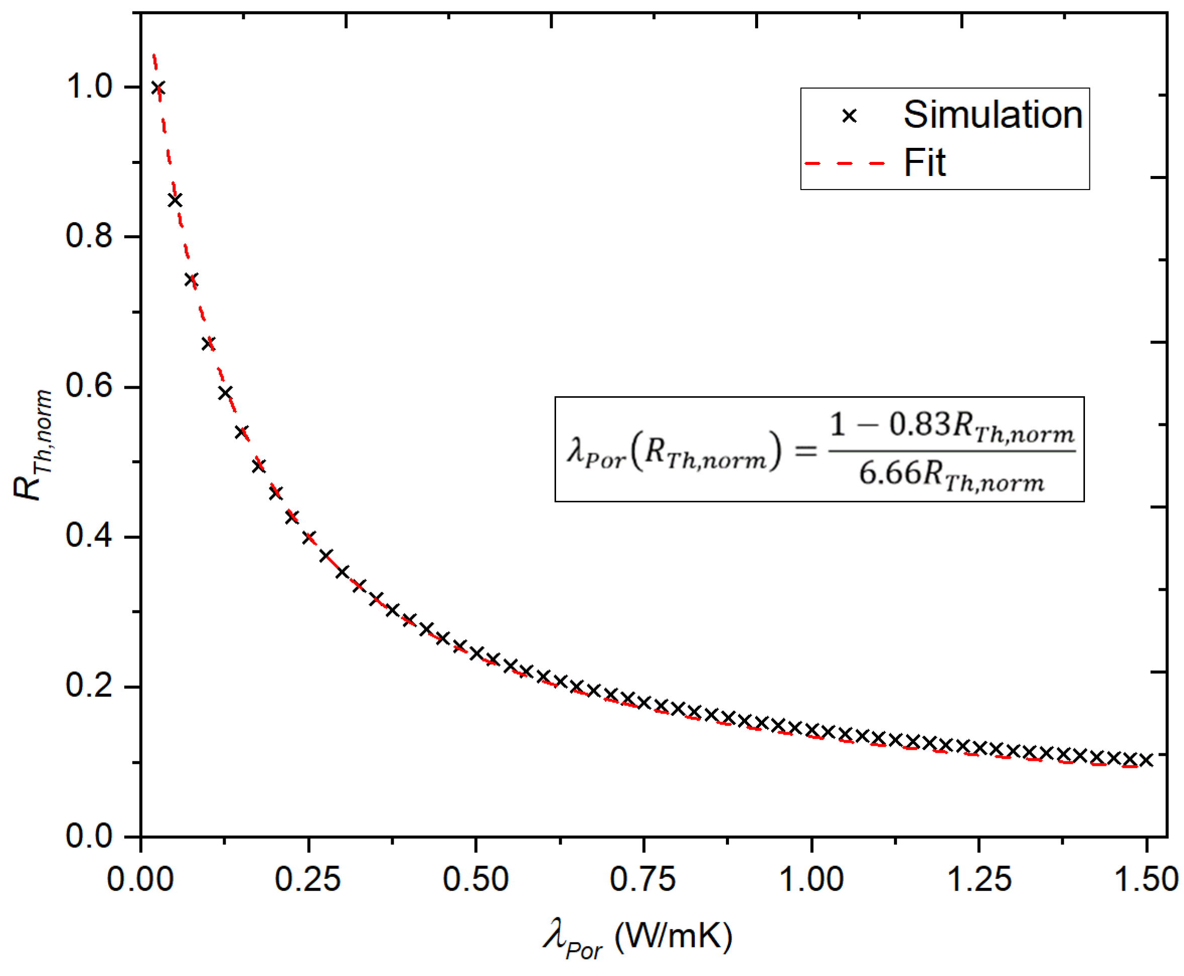
3.3.1. Quality of FEM Simulation and Fitting of Thermal Model
3.3.2. Estimation of Thermal Conductivity
4. Discussion
5. Conclusions
6. Patents
Author Contributions
Funding
Institutional Review Board Statement
Informed Consent Statement
Data Availability Statement
Acknowledgments
Conflicts of Interest
References
- Reyes-Romero, D.F.; Behrmann, O.; Dame, G.; Urban, G.A. Dynamic thermal sensor for biofilm monitoring. Sens. Actuators A Phys. 2014, 213, 43–51. [Google Scholar] [CrossRef]
- Dao, T.D.; Ishii, S.; Doan, A.T.; Wada, Y.; Ohi, A.; Nabatame, T.; Nagao, T. An On-Chip Quad-Wavelength Pyroelectric Sensor for Spectroscopic Infrared Sensing. Adv. Sci. (Weinh.) 2019, 6, 1900579. [Google Scholar] [CrossRef] [PubMed] [Green Version]
- Asri, M.I.A.; Hasan, M.N.; Fuaad, M.R.A.; Yunos, Y.M.; Ali, M.S.M. MEMS Gas Sensors: A Review. IEEE Sens. J. 2021, 21, 18381–18397. [Google Scholar] [CrossRef]
- Mukherjee, R.; Basu, J.; Mandal, P.; Guha, P.K. A review of micromachined thermal accelerometers. J. Micromech. Microeng. 2017, 27, 123002. [Google Scholar] [CrossRef] [Green Version]
- Gardner, E.L.W.; Vincent, T.A.; Jones, R.G.; Gardner, J.W.; Coull, J.; de Luca, A.; Udrea, F. MEMS Thermal Flow Sensors—An Accuracy Investigation. IEEE Sens. J. 2019, 19, 2991–2998. [Google Scholar] [CrossRef]
- Ejeian, F.; Azadi, S.; Razmjou, A.; Orooji, Y.; Kottapalli, A.; Ebrahimi Warkiani, M.; Asadnia, M. Design and applications of MEMS flow sensors: A review. Sens. Actuators A Phys. 2019, 295, 483–502. [Google Scholar] [CrossRef]
- Sinclair, M.J. A high force low area MEMS thermal actuator. In Proceedings of the Seventh Intersociety Conference on Thermal and Thermomechanical Phenomena in Electronic Systems (Cat. No.00CH37069), ITHERM 2000, Las Vegas, NV, USA, 23–26 May 2000; pp. 127–132. [Google Scholar] [CrossRef]
- Heo, S.; Kim, Y.Y. Optimal design and fabrication of MEMS rotary thermal actuators. J. Micromech. Microeng. 2007, 17, 2241–2247. [Google Scholar] [CrossRef]
- Hunter, S.R.; Lavrik, N.V.; Bannuru, T.; Mostafa, S.; Rajic, S.; Datskos, P.G. Development of MEMS Based Pyroelectric Thermal Energy Harvesters. Proc. SPIE 2011, 8035, 199–210. [Google Scholar] [CrossRef]
- Vonderschmidt, S.; Müller, J. A fluidic bridge based MEMS paramagnetic oxygen sensor. Sens. Actuators B Chem. 2013, 188, 22–30. [Google Scholar] [CrossRef]
- Lang, W.; Drost, A.; Steiner, P.; Sandmaier, H. The Thermal Conductivity of Porous Silicon. MRS Online Proc. Libr. 2011, 358, 561. [Google Scholar] [CrossRef]
- Kaltsas, G.; Nassiopoulos, A.A.; Nassiopoulou, A.G. Characterization of a silicon thermal gas-flow sensor with porous silicon thermal isolation. IEEE Sens. J. 2002, 2, 463–475. [Google Scholar] [CrossRef]
- Nassiopoulou, A.G.; Kaltsas, G. Porous Silicon as an Effective Material for Thermal Isolation on Bulk Crystalline Silicon. Phys. Stat. Sol. A 2000, 182, 307–311. [Google Scholar] [CrossRef]
- Sabate, N.; Keller, J.; Gollhardt, A.; Vogel, D.; Gracia, I.; Cane, C.; Morante, J.R.; Michel, B. 3D deformation analysis of flow and gas sensors membranes for reliability assessment. SPIE Proc. 2005, 5836, 416–424. [Google Scholar]
- Sabaté, N.; Gràcia, I.; Santander, J.; Fonseca, L.; Figueras, E.; Cané, C.; Morante, J.R. Mechanical characterization of thermal flow sensors membranes. Sens. Actuators A Phys. 2006, 125, 260–266. [Google Scholar] [CrossRef]
- Lisec, T.; Behrmann, O.; Gojdka, B. PowderMEMS—A Generic Microfabrication Technology for Integrated Three-Dimensional Functional Microstructures. Micromachines 2022, 13, 398. [Google Scholar] [CrossRef] [PubMed]
- Kostmann, C.; Lisec, T.; Bodduluri, M.; Andersen, O. Automated Filling of Dry Micron-Sized Particles into Micro Mold Pattern within Planar Substrates for the Fabrication of Powder-Based 3D Microstructures. Micromachines 2021, 12, 1176. [Google Scholar] [CrossRef] [PubMed]
- Ahmed, M.; Dankwort, T.; Grünzig, S.; Lange, V.; Gojdka, B. Broadband Zero-Power Wakeup MEMS Device for Energy-Efficient Sensor Nodes. Micromachines 2022, 13, 407. [Google Scholar] [CrossRef] [PubMed]
- Bodduluri, M.T.; Dankwort, T.; Lisec, T.; Grünzig, S.; Khare, A.; Ahmed, M.; Gojdka, B. Fully Integrated High-Performance MEMS Energy Harvester for Mechanical and Contactless Magnetic Excitation in Resonance and at Low Frequencies. Micromachines 2022, 13, 863. [Google Scholar] [CrossRef]
- Gojdka, B.; Cichon, D.; Lembrecht, Y.; Bodduluri, M.T.; Lisec, T.; Stahl-Offergeld, M.; Hohe, H.-P.; Niekiel, F. Demonstration of Fully Integrable Long-Range Microposition Detection with Wafer-Level Embedded Micromagnets. Micromachines 2022, 13, 235. [Google Scholar] [CrossRef]
- Bodduluri, M.T.; Gojdka, B.; Wolff, N.; Kienle, L.; Lisec, T.; Lofink, F. Investigation of Wafer-Level Fabricated Permanent Micromagnets for MEMS. Micromachines 2022, 13, 742. [Google Scholar] [CrossRef]
- Paesler, M.; Lisec, T.; Kapels, H. High Temperature Magnetic Cores Based on PowderMEMS Technique for Integrated Inductors with Active Cooling. Micromachines 2022, 13, 347. [Google Scholar] [CrossRef] [PubMed]
- Sonnick, S.; Meier, M.; Ross-Jones, J.; Erlbeck, L.; Medina, I.; Nirschl, H.; Rädle, M. Correlation of pore size distribution with thermal conductivity of precipitated silica and experimental determination of the coupling effect. Appl. Therm. Eng. 2019, 150, 1037–1045. [Google Scholar] [CrossRef]
- Knieling, T.; Laske, N.; Rasmussen, M.; Samson, J.; Muehler, T.; Behrendt-Fryda, B.; Blohm, L.; Nebling, E. Mikroozon—Thermal flow sensors and ozone generating electrodes for water cleaning applications. In Proceedings of the MikroSystemTechnik Congress 2019, Berlin, Germany, 28–30 October 2019. [Google Scholar]
- Simon, I.; Arndt, M. Thermal and gas-sensing properties of a micromachined thermal conductivity sensor for the detection of hydrogen in automotive applications. Sens. Actuators A Phys. 2002, 97–98, 104–108. [Google Scholar] [CrossRef]
- Eriksson, P.; Andersson, J.Y.; Stemme, G. Thermal characterization of surface-micromachined silicon nitride membranes for thermal infrared detectors. J. Microelectromech. Syst. 1997, 6, 55–61. [Google Scholar] [CrossRef]
- von Arx, M.; Paul, O.; Baltes, H. Process-dependent thin-film thermal conductivities for thermal CMOS MEMS. J. Microelectromech. Syst. 2000, 9, 136–145. [Google Scholar] [CrossRef]
- SCHOTT AG. Datasheet Borofloat 33. Available online: https://www.uqgoptics.com/wp-content/uploads/2019/07/Schott-Borofloat-33.pdf (accessed on 26 June 2022).
- Holmwood, R.A.; Glang, R. Resistivity and Temperature Coefficient of Pure Molybdenum. J. Chem. Eng. Data 1965, 10, 162–163. [Google Scholar] [CrossRef]
- Lisec, T.; Bodduluri, M.T.; Schulz-Walsemann, A.-V.; Blohm, L.; Pieper, I.; Gu-Stoppel, S.; Niekiel, F.; Lofink, F.; Wagner, B. Integrated High Power Micro Magnets for MEMS Sensors and Actuators. In Proceedings of the 2019 20th International Conference on Solid-State Sensors, Actuators and Microsystems & Eurosensors XXXIII (Transducers & Eurosensors XXXIII), Berlin, Germany, 23–27 June 2019; IEEE: Piscataway, NJ, USA, 2019. ISBN 9781538681046. [Google Scholar]


| Heater Substrate | Error (%) | ||
|---|---|---|---|
| Unmodified membrane | |||
| Glass |
| Gas Pressure | ||
|---|---|---|
| 0.1 MPa (Ambient) | ||
| 0.5 Pa (Vacuum chuck) |
| No. | Granted Patents | Short Description of the Patent Family |
|---|---|---|
| 1 | EP2670880B1 US9221217B2 JP6141197B2 | Fabrication of porous 3D microstructures, basic method |
| 2 | EP3523637B1 US11137364B2 | Thermal isolation based on porous 3D microstructures |
Publisher’s Note: MDPI stays neutral with regard to jurisdictional claims in published maps and institutional affiliations. |
© 2022 by the authors. Licensee MDPI, Basel, Switzerland. This article is an open access article distributed under the terms and conditions of the Creative Commons Attribution (CC BY) license (https://creativecommons.org/licenses/by/4.0/).
Share and Cite
Behrmann, O.; Lisec, T.; Gojdka, B. Towards Robust Thermal MEMS: Demonstration of a Novel Approach for Solid Thermal Isolation by Substrate-Level Integrated Porous Microstructures. Micromachines 2022, 13, 1178. https://doi.org/10.3390/mi13081178
Behrmann O, Lisec T, Gojdka B. Towards Robust Thermal MEMS: Demonstration of a Novel Approach for Solid Thermal Isolation by Substrate-Level Integrated Porous Microstructures. Micromachines. 2022; 13(8):1178. https://doi.org/10.3390/mi13081178
Chicago/Turabian StyleBehrmann, Ole, Thomas Lisec, and Björn Gojdka. 2022. "Towards Robust Thermal MEMS: Demonstration of a Novel Approach for Solid Thermal Isolation by Substrate-Level Integrated Porous Microstructures" Micromachines 13, no. 8: 1178. https://doi.org/10.3390/mi13081178
APA StyleBehrmann, O., Lisec, T., & Gojdka, B. (2022). Towards Robust Thermal MEMS: Demonstration of a Novel Approach for Solid Thermal Isolation by Substrate-Level Integrated Porous Microstructures. Micromachines, 13(8), 1178. https://doi.org/10.3390/mi13081178