Article

Bond Wire Damage Detection Method on Discrete MOSFETs Based on Two-Port Network Measurement

1
School of Mechanical and Electrical Engineering, Guilin University of Electronic Technology, Guilin 541004, China
2
Department of Microelectronics, Delft University of Technology, Mekelweg 4, 2628 CD Delft, The Netherlands
*
Authors to whom correspondence should be addressed.
Micromachines 2022, 13(7), 1075; https://doi.org/10.3390/mi13071075
Submission received: 11 June 2022 / Revised: 1 July 2022 / Accepted: 4 July 2022 / Published: 7 July 2022
(This article belongs to the Special Issue Advanced Packaging for Microsystem Applications)

Abstract

:
Bond wire damage is one of the most common failure modes of metal-oxide semiconductor field-effect transistor (MOSFET) power devices in wire-welded packaging. This paper proposes a novel bond wire damage detection approach based on two-port network measurement by identifying the MOSFET source parasitic inductance (LS). Numerical calculation shows that the number of bond wire liftoffs will change the LS, which can be used as an effective bond wire damage precursor. Considering a power MOSFET as a two-port network, LS is accurately extracted from frequency domain impedance (Z−parameter) using a vector network analyzer under zero biasing conditions. Bond wire cutoff experiments are employed to validate the proposed approach for bond wire damage detection. The result shows that LS increases with the rising severity of bond wire faults, and even the slight fault shows a high sensitivity, which can be effectively used to quantify the number of bond wire liftoffs of discrete MOSFETs. Meanwhile, the source parasitic resistance (RS) extracted from the proposed two-port network measurement can be used for the bond wire damage detection of high switching frequency silicon carbide MOSFETs. This approach offers an effective quality screening technology for discrete MOSFETs without power on treatment.

1. Introduction

Power electronic devices are widely used in mission-critical applications, such as locomotive traction, high-speed railway, electric vehicles, industrial frequency conversion, and renewable energy generation [1,2]. Literature studies indicated that the failure rate of power electronic devices among all converter failure types is 31%, accounting for the largest proportion among all failure types [3,4]. High-power metal-oxide semiconductor field-effect transistor (MOSFET) is one of the most critical and fragile elements in power electronic devices operating in harsh and uncertain conditions. MOSFETs will suffer from continuous excessive electrical–thermal–mechanical stresses and damage the bond wires and the solder layer. The reliability of MOSFETs has been attracting increasing research interest. In practical applications, the fatigue failure of power semiconductor devices in wire welding packaging is mostly manifested as the bond wires completely liftoff [1,5,6,7,8]. Therefore, the quality detection of MOSFET bond wire is of considerable importance to avoid the catastrophic failure of power electronic converters in the lifecycle.
Middle- and high-power MOSFETs are generally based on wire-welded packaging, which uses some parallel aluminum bond wires to improve the current carrying capacity for electrical interconnections between drain and source terminals. This condition introduces a problem that cannot be ignored; that is, the slight fault of bond wires will not immediately affect the performance of MOSFETs, which increases the difficulty of bond wire damage detection. Numerous research papers indicated that the commonly used bond wire reliability detection methods can be classified into two: degradation precursor- and morphology characteristic-based methods. Degradation precursor-based methods usually predict bond wire damage by measuring different types of signals and comparing them with the healthy device. These methods can be classified into the following three classes according to the type of signals used: voltage, current, and other signal precursor-based approaches. The first class is the voltage precursor-based approach. On-state drain-source (VDS) [8], collector–emitter saturated voltage (VCE(sat)) [9], gate threshold voltage (Vth) [10], and turn-on gate voltage overshoot [5] are selected as bond wire fault indicators. Measuring the voltage signal is usually easy, and the sensitivity is minimal when the bond wire faults are minor. Moreover, the accuracy of the measurement is easily affected by the changes in bus voltage, current, and chip junction temperature; thus, strictly ensuring the high consistency of test conditions in each measurement is necessary. The second class is the current precursor-based approach. Gate current (IG) [11] and short-circuit current (ISC) [12,13] are usually selected as bond wire fault indicators. Reference [14] indicates that ISC is sensitive to bond wire failures but requires accurate control of gate-drive voltage and junction temperature (Tj) in measurement, which adds complexity to applications. Reference [15] found that the bond wire liftoff has minimal influence on the dynamic differences of IG. A high-precision A/D converter with a high sampling rate is needed to improve sampling precision, however using such a converter in the gate driver is too expensive. The third class is the other signal precursor-based approaches, including junction temperature (Tj) [16], thermal resistance from junction to case (Rth) [17], on-resistance (RDS(on)) [18], Miller plateau duration (VGP) [19], and others. RDS(on) and Rth belong to temperature-dependent parameters, and the measurement accuracy is affected by the junction temperature, Tj. Unfortunately, Tj cannot be measured directly, and the stable control of Tj is also a technical problem. Miller plateau duration has minimal sensitivity when one or two bond wires liftoff. Morphology characteristic-based methods mainly include thermal imaging [20,21,22,23] (eddy current pulse thermal imaging, infrared imaging) and structural imaging [24,25,26] (X-ray imaging, ultra-sound imaging, and industrial computerized tomography). Thermal imaging can identify the location of potential damage by observing the surface temperature distribution of the power devices, which is mainly used to detect solder-layer defects. Structural imaging is a non-destructive testing technology and can directly detect inner defects of devices by identifying the phase and amplitude of the reflected signals. However, the key to obtaining the ideal imaging quality lies in the accurate height estimation of the bond wire in the Z-axis direction in advance by the users, which is a remarkably difficult and time-consuming task. If delamination exists between the epoxy molding compound (EMC) layer and the upper surface of the die, then penetrating the EMC for effective bond wire imaging is difficult for the pulse ray, resulting in a limited application.
A novel bond wire damage detection approach based on two-port network measurement by identifying the MOSFET source parasitic inductance (LS) is proposed in this study. Based on frequency domain impedance analysis, MOSFET is equivalent to some second-order RLC circuits comprising independent inductances, capacitances, and resistances in series, whereas the high-frequency impedance of MOSFET is dominated by the inductive components. Therefore, the bond wire is equivalent to the pure inductance model at a frequency much higher than the self-resonant frequency (fSRF). The liftoff of the bond wire will increase the total parasitic inductance of the parallel bond wires, resulting in increasing high-frequency impedance. This notion provides a new idea that the physical failure of the bond wire can be mapped to the change in high-frequency impedance. Considering a power MOSFET as a two-port network, LS is accurately extracted from vector network analyzer (VNA) measurement under zero basing conditions. The positive correlation between the LS and the number of bond wire faults is then determined. The experimental results reveal that even a slight bond wire fault can be detected with high resolution. This method offers an effective bond wire damage detection technology for power-discrete devices without power on treatment.

2. Methodologies

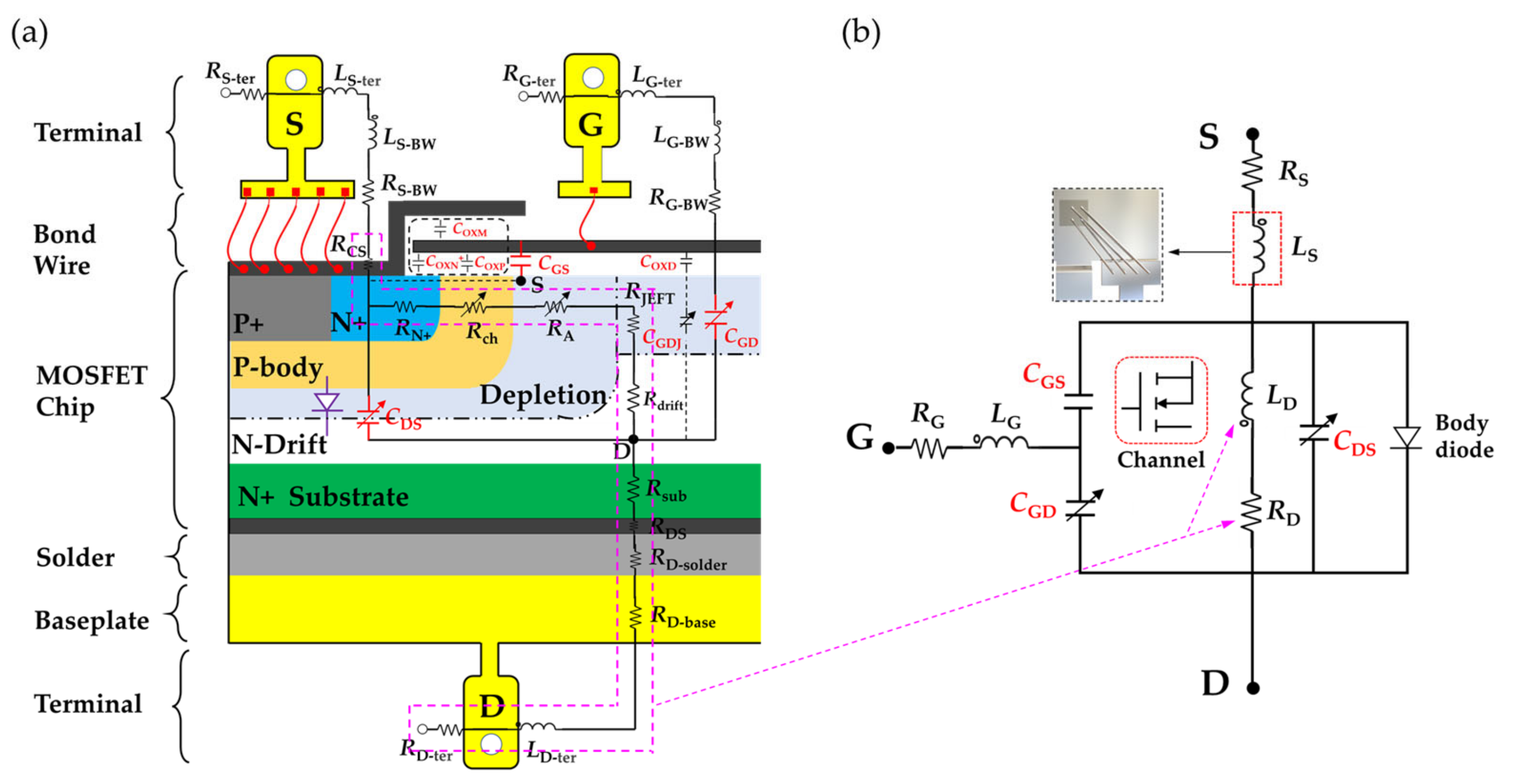
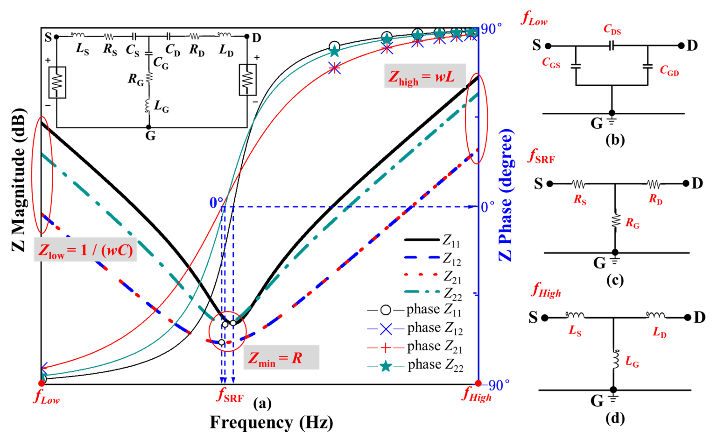
2.1. MOSFET Small-Signal Equivalent Circuit

The schematic of a cross-section of a half-vertical-diffused MOSFET with a package structure is illustrated in Figure 1a. An ideal MOSFET chip can be equivalent to the constant and variable active devices, which comprise the voltage-controlled current source, internal parasitic capacitances, and anti-parallel body diode. The internal parasitic capacitances include drain–source capacitance (CDS), gate–source capacitance (CGS), and gate–drain capacitance (CGD). The chip and external terminals are electrically interconnected through the aluminum bond wire packaging technology. Additional parasitic parameters are inevitably introduced: (1) LS-ter and LG-ter, LD-ter and RS-ter, and RG-ter and RD-ter are generated from the gate, source, and drain terminals, respectively. (2) LS-BW, LG-BW, and RS-BW, RG-BW are generated from bond wires. (3) RD-solder and RD-base are generated from the solder and baseplate layers, respectively. The small-signal equivalent circuit model is simplified. The parasitic inductances are combined into LG, LS, and LD and the parasitic resistors into RS, RG, and RD to facilitate the analysis, as shown in Figure 1b. Figure 2 depicts a typical power MOSFET in a TO−247 discrete package, which is encapsulated by a chip, copper substrate, bond wires, lead terminals, solder layer, and an EMC. The equivalent circuit of the MOSFET power device is decomposed in sequence according to the drain-to-source current loop.

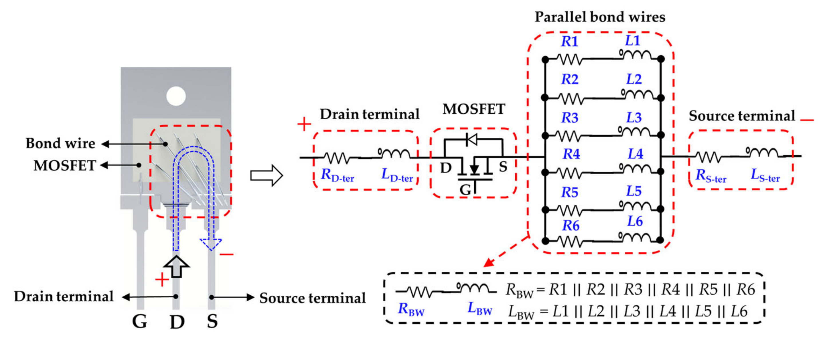
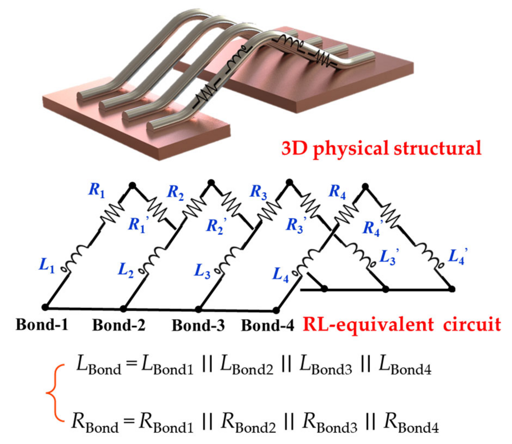
2.2. Bond Wire Parasitic Inductance

MOSFETs in wire-welding packaging comprise multilayered materials with different coefficients of thermal expansion (CTE). Long-term thermal stress causes the expansion of different materials at various rates, specifically in the weak points of the wire bond root, resulting in bond wire fatigue and degradation. Figure 3 shows a 3D structural diagram of the four parallel bond wires, wherein each bond wire can be equivalent to a set of RL series circuits. The partial inductance, LBond, of a bond wire comprises partial self and mutual inductances. According to [27], the self-inductance, L (in nH), of a single bond wire can be extracted by the simplified Equation (1), and the parasitic mutual-inductance, M (in nH), of a single bond wire can be determined by the simplified Equation (2).
L = 5 l ×   [ ( In ( 4 l / d ) 0.75 ) ] ,
M = 5   ×   [ In ( 2 l s )     1   +   s l     ( s 2 l ) 2 ] ,
where l stands for the length of the bond wire (in inches), d stands for the diameter of the bond wire (in inches), and s stands for the distance between two bond wire centers (in inches). The mutual inductance for multiple bond wires is caused by the magnetic coupling of multiple bond wires. The internal structure and bond wire dimension of IXFK32N100P (IXYS Corporation, Milpitas, CA, USA and Leiden, The Netherlands) and C2M0160120D (Wolfspeed Corporation, Durham, NC, USA) are shown in Figure 4 and Table 1. Each bond wire is marked with a serial number for easy identification.
For IXFK32N100P, the parasitic inductance of bond wire No. 1, LBond_1, lies in the addition of bond wire self-inductance L1 and mutual inductances M12, M13, M14, M15, and M16. Similarly, the parasitic inductance of bond wire No. 2, LBond_2, lies in the addition of bond wire self-inductance L2 and mutual inductances M21, M23, M24, M25, and M26. The parasitic inductance of other bond wires is calculated by the same method. Therefore, the bond wire parasitic inductance, LBond_m, of No. m is the sum of bond wire self-inductance Lm of No. m (calculated by Equation (1)) and bond wire mutual inductances Mmn between No. m and No. n (calculated by Equation (2)), which can be described as follows:
L Bond _ m   = L m   + n = 1 n M m n   ( m     n )
Figure 4 shows that the multiple bond wires of discrete MOSFETs are not strictly parallel to each other. To simplify the calculation, the non-parallel distribution of the parallel connection bond wires between the source and source terminal is ignored, and the average spacing between the two bond wires and the length of the short bond wire is selected for mutual inductance estimation. The parasitic inductance, LBond, is calculated and shown in Table 2. The total parasitic inductances of IXFK32N100P, LBond_IX, and C2M0160120D, LBond_C2, are correspondingly 4.33 and 3.75 nH, which are the results of parallel connections of six and four inductances, respectively.

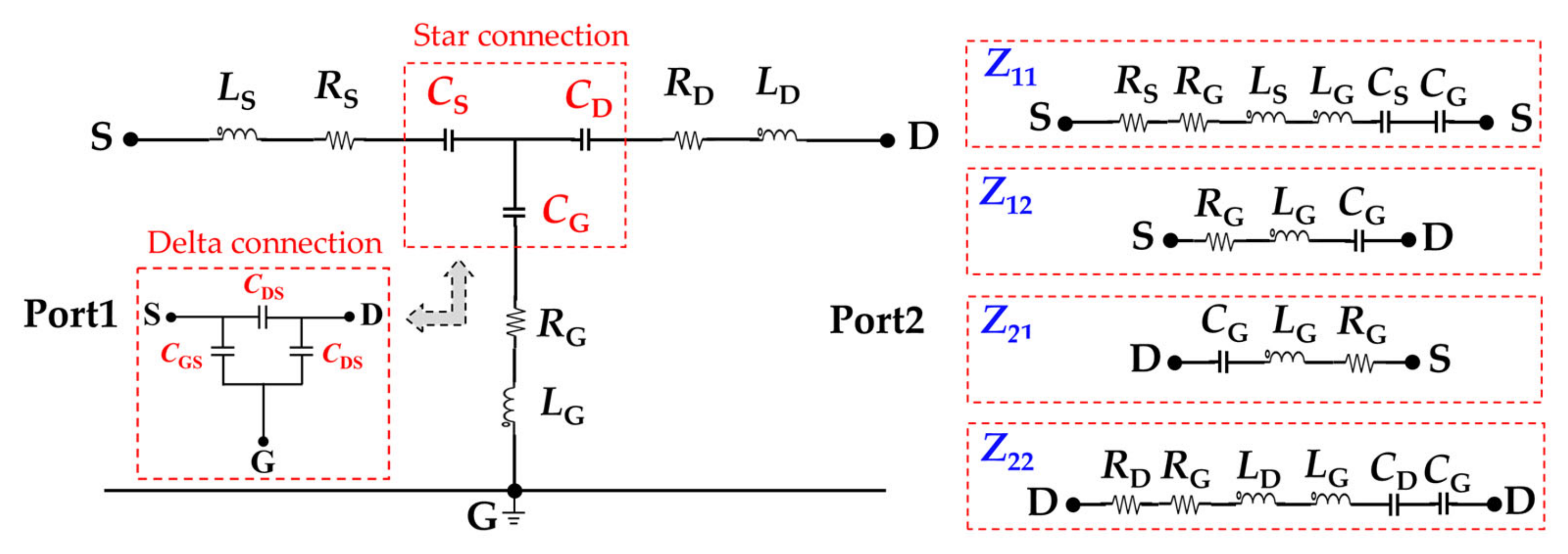
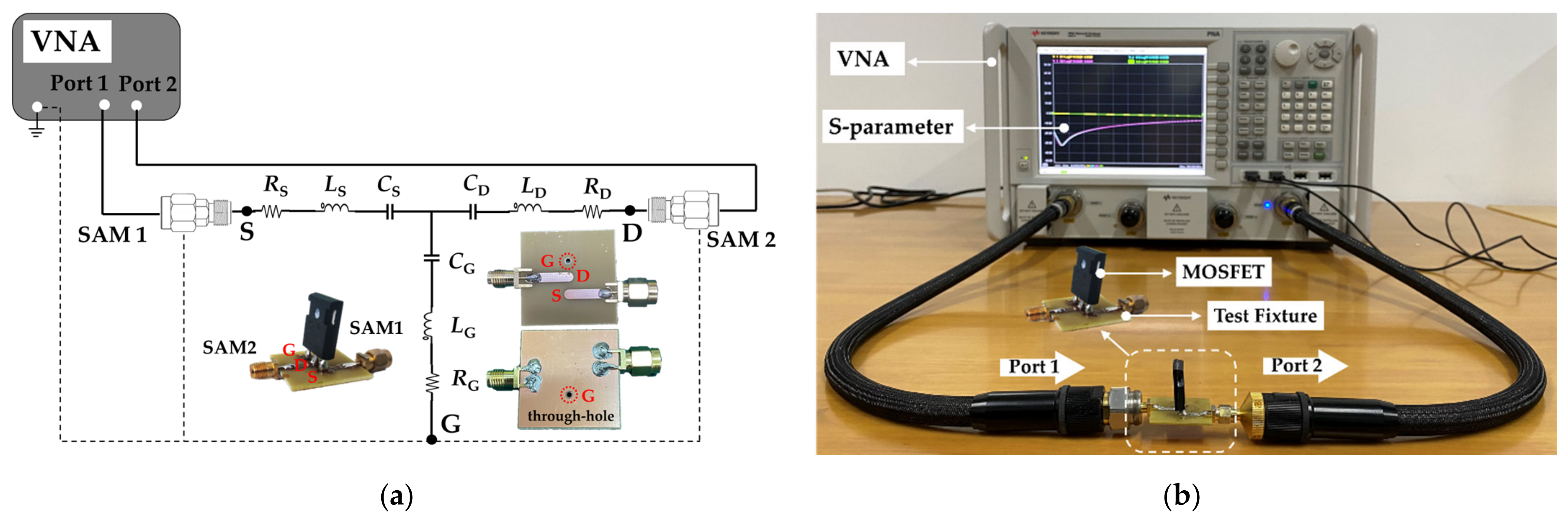
2.3. Two-Port Parasitic Inductance Extraction Approach

The two-port scattering (S) parameter measurement with VNA is used in this study to extract the parasitic parameters of MOSFET [28,29]. The MOSFET small-signal equivalent circuit under zero biasing conditions, which is a two-port network with S–G and D–G as Ports 1 and 2, respectively, is shown in Figure 5. Each of the two-port network Z−parameters, Z11, Z12, Z21, and Z22, can be equivalent to some second-order RLC circuits comprising independent inductances, capacitances, and resistances in series. Z11 is equivalent to the LSRSCSCGRGLG series circuit, Z12 and Z21 are equivalent to the same GGRGLG series circuit, and Z22 is equivalent to the LGRGCGCDRDLD series circuit. Notably, as a standard form of the two-port network, the equivalent capacitances (CG, CD, and CS) demonstrate a star connection in Figure 5, which is different from the delta connection of parasitic capacitances (CGS, CDS, and CGD) in Figure 1b. Therefore, the star connection should be converted into a delta connection by using Equations (4)–(6) to extract the parasitic capacitances.
C GS   =   C G C S   / ( C G + C D   + C S ) ,
C GD   =   C G C D   / ( C G + C D   + C S ) ,
C DS   =   C D C S   /   ( C G + C D   + C S ) .
Figure 6 shows a typical impedance plot of a MOSFET small-signal equivalent circuit with predetermined parameters. A set of typical values for the parasitic inductances (LG = 15 nH, LD = 20 nH, and LS = 30 nH), parasitic capacitances (CS = 5 nF, CD = 10 nF, and CG = 15 nF), and resistances (RG = 1.5 Ω, RD = 0.5 Ω, and RS = 0.5 Ω) is presented in the Advanced Design System (ADS) simulation setup with a frequency sweep from 1 to 300 MHz. The ADS simulated magnitude and phase angle of impedance (Z) parameters are shown in Figure 6a. Z11, Z12, Z21, and Z22 of the series RLC circuit can be calculated using Equations (7)–(9). The effect of capacitive reactance and resistance can be neglected at high frequency, fHigh (endpoint of the frequency range). Therefore, the two-port network representation of the MOSFET equivalent circuit can be simplified as shown in Figure 6d. The high-frequency impedance is dominated by the inductive reactance, and the parasitic inductances LS, LG, and LD can be calculated through Equations (10)–(12). At the fSRF, inductive and capacitive reactance cancel each other, and the impedance magnitude has its minimum value. The two-port network representation of the MOSFET equivalent circuit can be simplified as shown in Figure 6c. The parasitic resistances RS, RG, and RD can be determined at the fSRF through Equations (13)–(15). Meanwhile, the effect of inductive reactance and resistance can be neglected at low frequency, fLow (starting point of the frequency range). Therefore, the two-port network representation of the MOSFET equivalent circuit can be simplified as shown in Figure 6b. The equivalent capacitances CG, CS, and CD are respectively determined by plugging the extracted LS, LG, and LD into Equations (16)–(18). Finally, the capacitor star connection is converted to a delta connection through Equations (4)–(6) to extract parasitic capacitances CGS, CGD, and CDS.
Z 11 = X L S + X L G + X R S + X R G + X C S + X C G   ,
Z 12 = Z 21 = X L G   + X R G + X C G   ,
Z 22   = X L D + X L G + X R D + X R G + X C D + X C G   ,
L S + L G = i m a g   ( Z 11 _ High )   /   w 11 _ High   ,
L G = i m a g   ( Z 12 _ High )   /   w 12 _ High   ,
L D + L G = i m a g   ( Z 22 _ High )   /   w 22 _ High   ,
R S + R G = Z 11 _ min   ,
R G = Z 12 _ min   ,  
R D + R G = Z 22 _ min   ,
C S C G C S + C G = 1   /   [ w 11 _ SRF 2   ·   ( L S   + L G ) ]   ,
C G = 1   /   ( w 12 _ SRF 2   ·   L G )   ,
C D C G C D + C G = 1   /   [ w 22 _ SRF 2   ·   ( L D   + L G ) ]   .

3. Experimental Results and Discussion

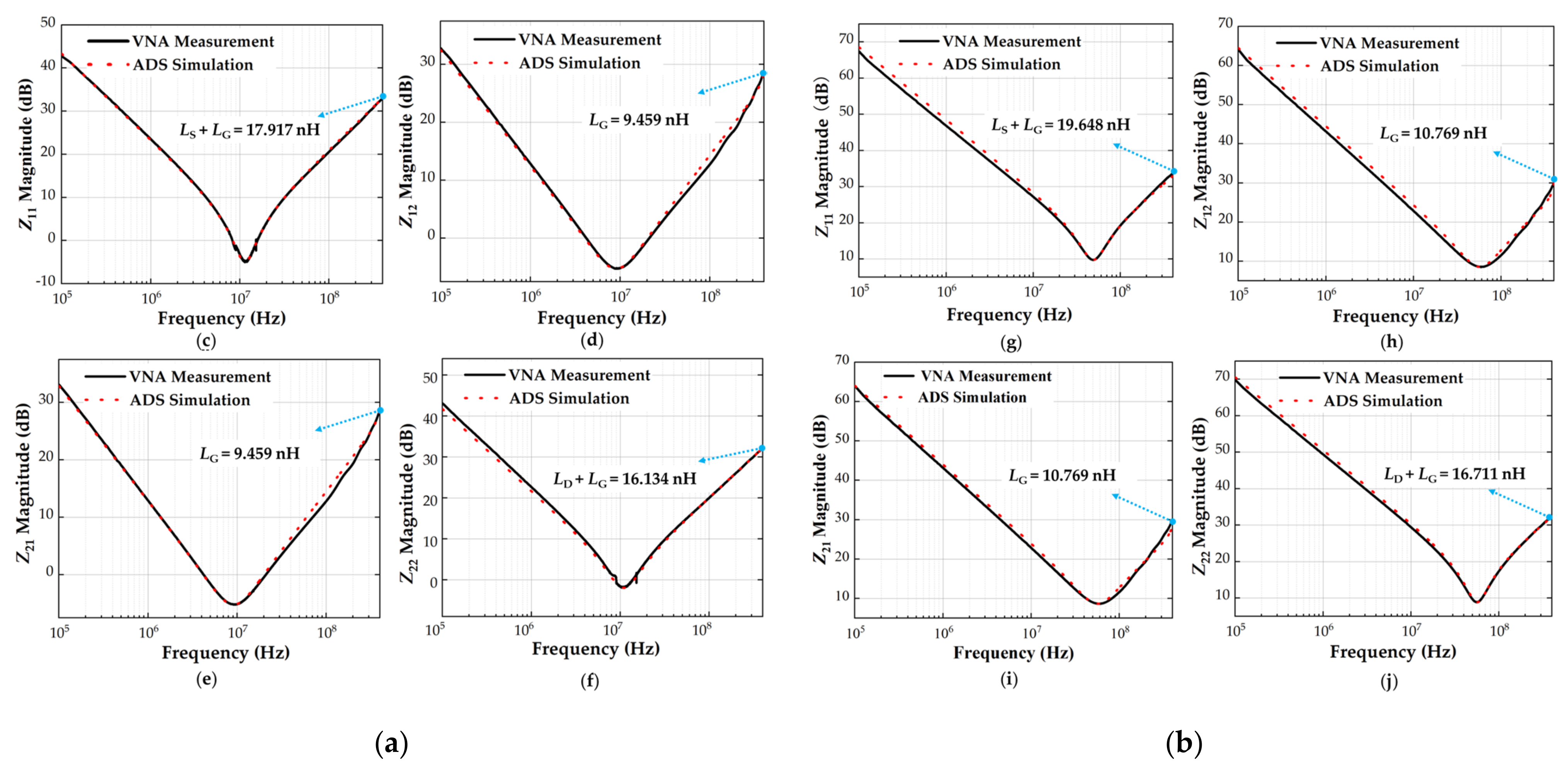
3.1. Validation Parasitic Inductance Extraction Approach for MOSFET

A 1000 V Si MOSFET (IXFK32N100P in TO−247 package) and a 1200 V SiC MOSFET (C2M0160120D in TO−247 package) were used in this paper to verify the two-port network measurement technique. Figure 7 shows the schematic of the two-port network model and the VNA measurement system. An additional test fixture [30], which reserves three connection positions and ensures the low-inductance connections between VNA and terminals, must be designed to ensure the effective connection between MOSFET and VNA. The test fixture shall have a negligible loss, good impedance match (50 Ω), and high isolation between input and output. The printed circuit board (PCB) test fixture comprises two 50 Ω SMA adaptors, two 50 Ω microstrip lines, and a through-hole, as shown in Figure 7a. The top copper layer of the PCB is graphically processed into two 50 Ω microstrip lines. The bottom copper layer of the PCB is reserved for interconnection with the VNA ground. The MOSFET was installed on the PCB test fixture and connected with VNA through SMA. The MOSFET source terminal is interconnected with VNA port 1, the MOSFET drain terminal is interconnected with VNA port 2, and the gate terminal is interconnected with the VNA ground through a PCB through-hole. De-embedding calibration [31] was performed to remove the systematic errors caused by test cables, adapters, and fixtures before VNA measurement. The 80502D calibration kit (Keysight, Santa Rosa, CA, USA) provided by Keysight was used in this study to perform the short-open-load VNA calibration. A new “through” calibration element based on a PCB test fixture was designed to replace the “through” calibration element in the 80502D kit to extend the measurement plane from SAM coaxial connected to the interface of the device plane.
ADS circuit simulation was used to validate the proposed two-port parasitic inductance extraction methodology. First, the S−parameter of the MOSFET was obtained from VNA measurement and converted into Z−parameters. Then, the parasitic inductances, capacitances, and resistances were accurately calculated from Z−parameters through Equations (10)–(18). Finally, the extracted parasitic parameters were plugged back into the small-signal equivalent circuit of the power MOSFET for ADS simulation over a frequency range of 100 kHz to 400 MHz (the frequency range is not strictly fixed and can be adjusted according to different MOSFETs). Figure 8 shows the frequency response curves of the Z−parameters obtained from ADS simulation and VNA experimental measurement. The ADS simulation curve (red dashed line) was found to be in good agreement with the experimental value (black solid line) in Si and SiC MOSFETs, which indicates that the derived parasitic parameter extraction mathematical formulas (Equations (10)–(18)) and extraction methodology mentioned in Section 2.3 are effective and correct. A through-hole must be set on the PCB test fixture to connect the MOSFET gate terminal to the VNA ground. Unfortunately, through-hole will cause unwanted signal reflection on the transmission path, resulting in a slight impedance mismatch between the simulation and measurement of Z12 and Z21 at frequencies above the fSRF. LS is calculated by subtracting Equation (10) from Equation (11). Thus, the gate parasitic inductance, LG, and the impedance mismatch introduced by through-hole can be excluded from the calculation. In addition, the secondary validation approach was realized by comparing the parasitic capacitances extracted from the proposed approach with the device datasheet values. The parasitic capacitances of the SiC MOSFET (C2M0160120D) obtained from the proposed two-port extraction technique were 0.49, 0.27, and 0.55 nF. Considering the unavoidable measurement error, the extracted capacitances were consistent with the datasheet values reported in [29] (CGS = 0.47 nF, CGD = 0.28 nF, and CDS = 0.51 nF, f = 1 MHz), and the mismatch was 4.25%, 3.57%, and 7.84%. The experimental results show that the proposed two-port extraction methodology is suitable for accurately extracting the parasitic inductance of discrete-power MOSFETs.

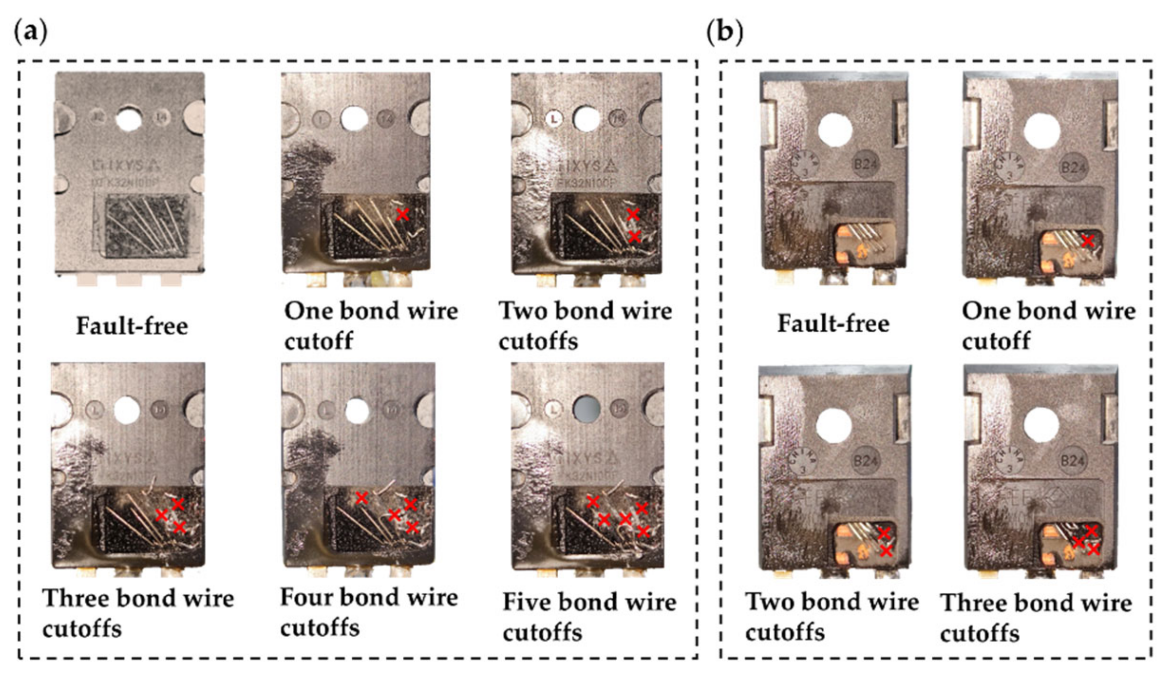
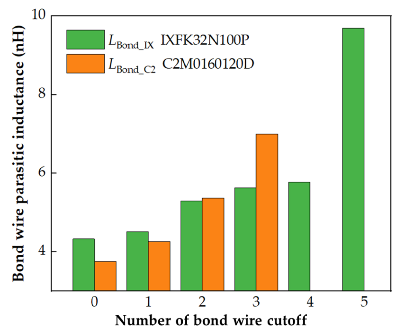
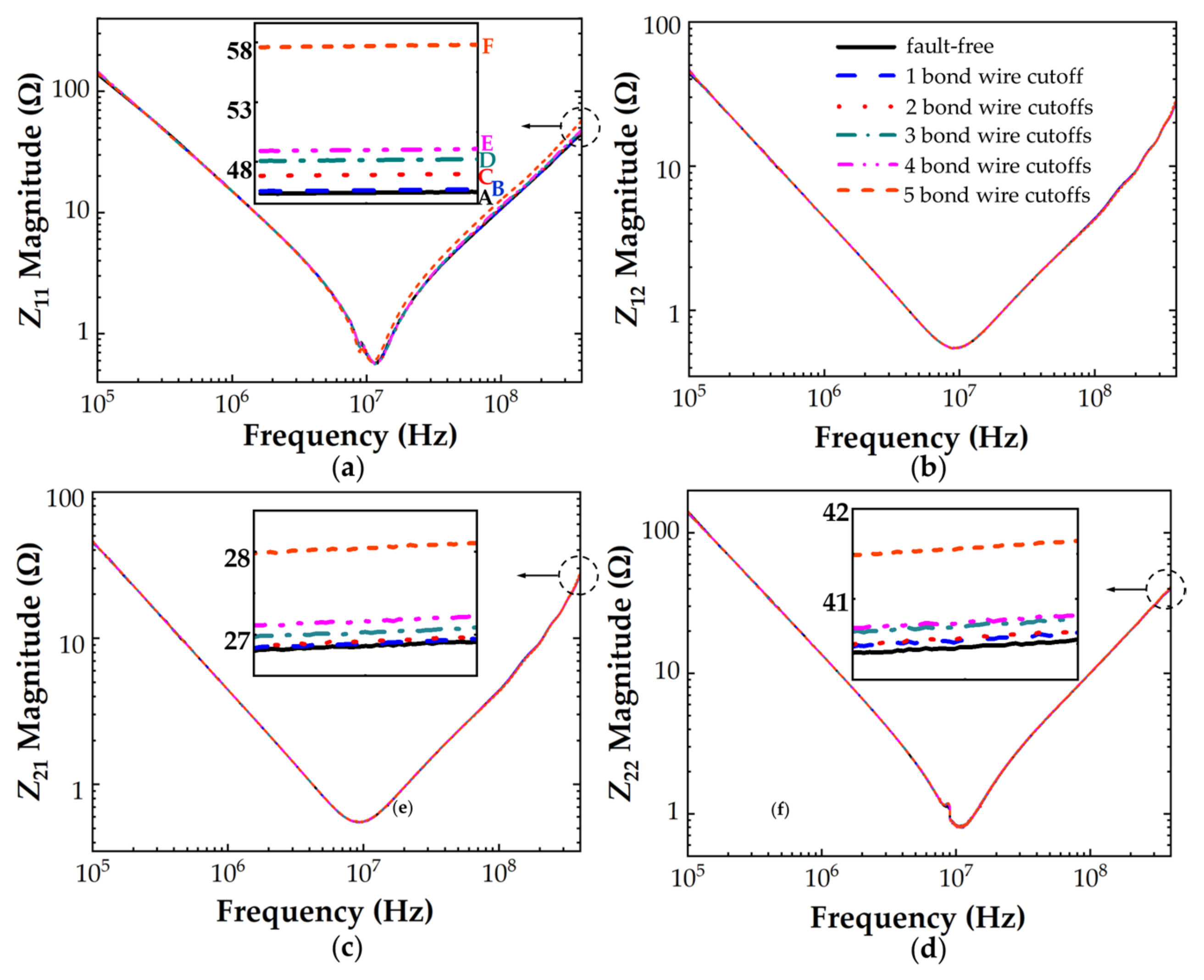
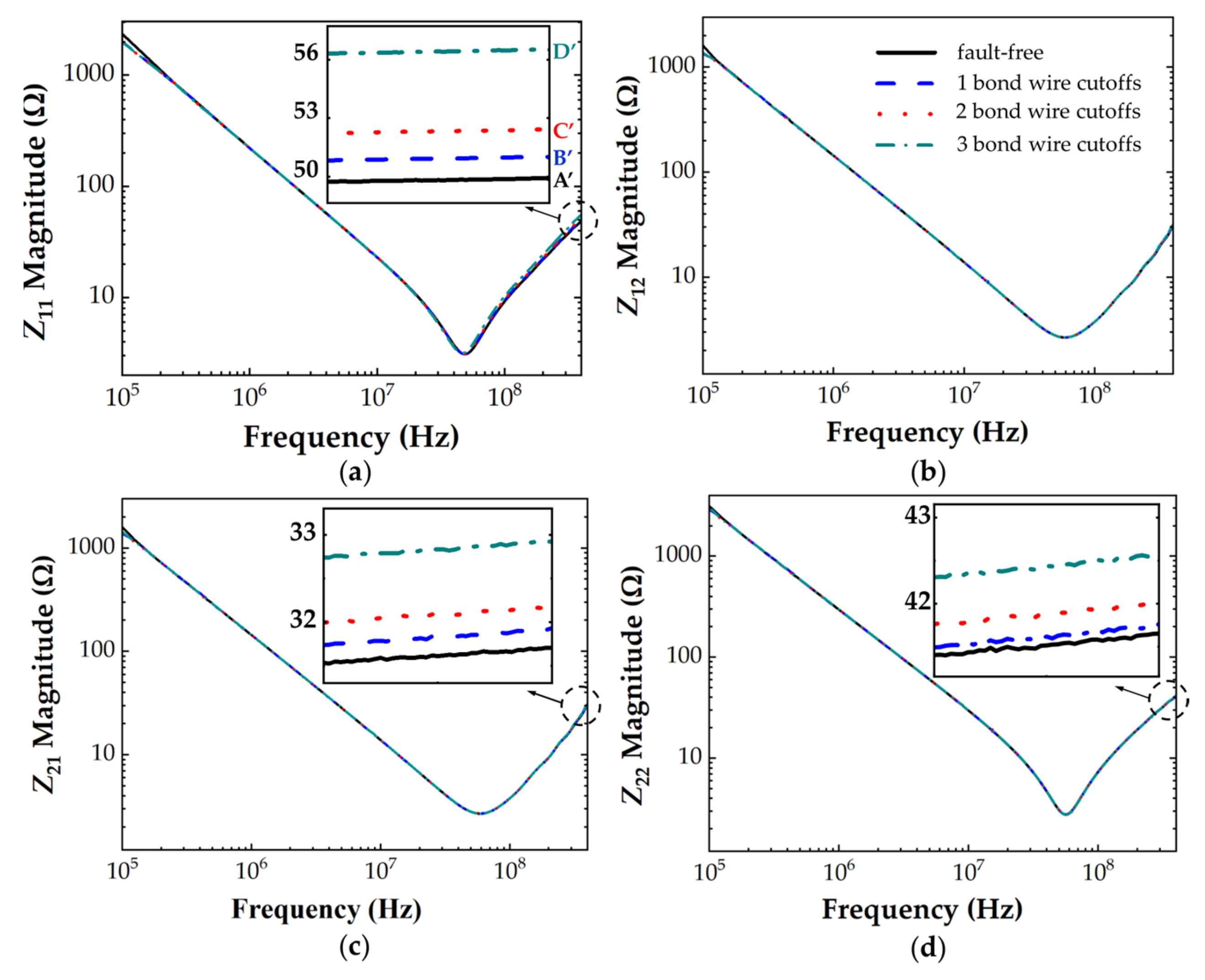
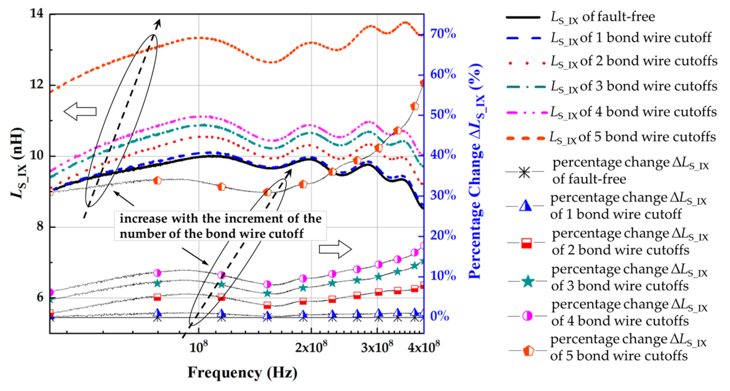
3.2. Analysis of Parasitic Inductance with Bond Wire Fault

This paper aims to provide a precursor for bond wires’ degradation. The current study used the approach of cutting off bond wires to simulate their faults to shorten the duration of experimental tests. Laser equipment was used to remove the epoxy layer of the power device to expose the bond wires completely. The bond wire damage models were then established by manually cutting off the bond wires individually. The damage models of IXFK32N100P and C2M0160120D are shown in Figure 9.
When one bond wire is cut off (for instance, No. 1), the bond wire self-inductance L1 and mutual inductances M1n and Mm1 (M12, M13, M14, M15, and M16, and M21, M31, M41, M51, and M61, are generated by the magnetic coupling between bond wire No. 1 and other bond wires Nos. 2–6, respectively) no longer exist. The parasitic inductances of other valid bond wires (Nos. 2–6) are calculated by Equations (1)–(3), described in Section 2.2, and summarized in Table 3. The total parasitic inductance of IXFK32N100P is 4.51 nH, which is attributed to the result of the parallel connection of the five remaining bond wires. The total parasitic inductance of C2M0160120D is 4.26 nH, which is the result of the parallel connection of the three remaining bond wires. Similarly, for other bond wire damage models, such as cutting off two bond wires (Nos. 1 and 2), cutting off three bond wires (Nos. 1, 2, and 3), cutting off four bond wires (Nos. 1, 2, 3, and 4), and cutting off five bond wires (Nos. 1, 2, 3, 4, and 5), the parasitic inductances are calculated from Equations (1)–(3), and listed in Appendix A, Table A1, Table A2, Table A3 and Table A4. The corresponding relationship between parasitic inductance, LBond, and the number of cutoff bond wires is shown in Figure 10. For ease of description, the liftoff of one or two bond wires is defined as “slight fault” and that of three or more bond wires is “serious fault.” Each of the total bond wire parasitic inductances of IXFK32N100P and C2M0160120D are positively correlated with the number of the bond wire cutoff. For slight fault, the percentage changes of LBond_IX in IXFK32N100P were 4.16% and 22.40%, while those of LBond_C2 in C2M0160120D were 13.60% and 43.20%, showing high sensitivity. These results indicate that the proposed bond wire damage detection approach is reasonable. Figure 10 indicates that the parasitic inductance, LBond, rises with the increase in the number of bond wire cutoffs, which can be potentially used as a precursor of bond wire damage. However, the parasitic inductance generated by the source terminal is not considered in the numerical analysis. The source parasitic inductance extracted from the two-port network measurement includes the bond wire parasitic inductance and the source terminal parasitic inductance. The sensitivity of MOSFET source parasitic inductance with various bond wire cutoffs is discussed in the following.

3.3. Bond Wire Experimental Results

The S−parameters of the bond wire damage models were measured with the VNA over a frequency range of 100 kHz to 400 MHz and then converted to Z−parameters. Figure 11 shows the Z−parameter frequency response curves of IXFK32N100P Si MOSFET with various bond wire faults. At frequencies above the fSRF, Z11 (Z11_High = LS + LG) increased with the number of bond wire cutoffs, whereas Z12 (Z12_High = LG), Z21 (Z21_High = LG), and Z22 (Z22_High = LG + LD) changed by less than 1 Ω when five bond wires were cutoff. This finding indicates a strong positive correlation between the damage of bond wires and the increase in source parasitic inductance, which is consistent with the presented theoretical expectation. The ratios expressed as percentage changes were calculated to define the degree of bond wire degradation. Percentage changes in Z11 and LS are the different ratios of the measured value with the actual device compared with the initial value of the fault-free device under testing. For IXFK32N100P, the percentage changes in Z11 parameters of each bond wire damage model were 0.51%, 3.52%, 6.46%, 8.46%, and 28.95% at 400 MHz. For C2M0160120D, the Z−parameter frequency response curves are shown in Figure 12. This finding has a similar change trend as in Figure 11 with the increase in the number of bond wire cutoffs. The percentage changes of Z11 at 400 MHz were 2.46%, 5.60%, and 14.72%.
Figure 13 and Figure 14 show that the source parasitic inductance increased with the increment of the number of the bond wire cutoffs, which is consistent with the change in LBond obtained by numerical calculation (Appendix A, Table A1, Table A2, Table A3 and Table A4). The parasitic inductance and resistance with various bond wire cutoffs are shown in Table 4. MOSFET is equivalent to the inductive element when the frequency is larger than the fSRF. With the increase in frequency, the skin effect forces the increase in parasitic resistance of the conductors (such as bond wire and terminal) and the reduction in parasitic inductance. For IXFK32N100P, the percentage change in the source parasitic inductance LS_IX significantly increased with the increment of the number of bond wire cutoffs, and the difference reached the maximum at 400 MHz. With bond wire cutoffs varying from 1 to 5, the LS_IX at 400 MHz increased from 8.52 to 8.61, 9.20, 9.71, 10.03, and 13.46 nH, and the percentage changes were 1.12%, 7.96%, 13.98%, 17.75%, and 58.02%, respectively. However, the extracted source parasitic resistance RS_IX did not show the expected regular increase with the rising severity of bond wire faults. This phenomenon is due to the excessively low fSRF of IXFK32N100P (≈9 MHz) to identify the RS_IX (<0.015 Ω) effectively. Similarly, for C2M0160120D, the percentage change of source parasitic inductance LS_C2 has the maximum difference at 400 MHz. With bond wire cutoffs varying from 1 to 3, the LS_C2 at 400 MHz increased from 8.88 to 9.30, 9.85, and 11.43 nH, and the percentage changes were 4.71%, 10.97%, and 28.79%, respectively. SiC MOSFET has a higher switching frequency than traditional Si-based power semiconductor devices. The fSRF of C2M0160120D is close to 58 MHz. Thus, the skin effect induced the increment of source parasitic resistance RS_C2 to more than 0.400 Ω, which reduced the identification accuracy requirements of RS_C2 by an order of magnitude, facilitating its accurate identification. The measurement results of the percentage change of RS_C2 with various bond wire cutoffs were 1.35%, 4.24%, and 17.21%, indicating that RS_C2 can be used as another precursor for bond wire fault detection. However, Table 4 shows that the resolution of RS_C2 was lower than that of LS_C2 in a two-port VNA measurement. If the fSRF of MOSFET is low, then the influence of the skin effect on the conductor is not observed. Thus, the source parasitic resistance is too small to be accurately identified. Therefore, the source parasitic resistance can only be used to identify the bond wire damage of high switching frequency MOSFETs, especially in emerging wide-bandgap SiC MOSFETs.
The bond wire parasitic inductances obtained by numerical calculation and the source parasitic inductance extracted from VNA measurement are compared in Figure 15. The parasitic inductances obtained by the two approaches have a similar trend with the increase of the number of bond wire cutoffs. For the two MOSFETs, the difference in parasitic inductance between numerical calculation and VNA measurement was maintained at ∆LC2 = 4.1 ± 0.3 nH and ∆LIX = 4.7 ± 0.3 nH, respectively. This difference can be attributed to the following two reasons: (1) VNA-measured Z−parameters include source terminal parasitic inductance, which is the main reason for the difference, as shown in Figure 15. (2) The spacing between two bond wires is taken as the average value to simplify the mutual inductance numerical calculation. Therefore, the VNA measurement extracted values are consistent with the numerically calculated values considering the fixed difference (∆LC2 and ∆LIX). The comparison results further verify the effectiveness of the proposed method of extracting the parasitic inductance from VNA measurement by considering a power MOSFET as a two-port network.
The change in source parasitic inductance can be accurately distinguished regardless of a “slight fault” or “serious fault.” Thus, the proposed bond wire damage detection approach in this paper has high discrimination. In addition, the parasitic parameters were extracted under zero DC biasing voltage (off-state) based on the two-port network VNA measurement, which can effectively avoid the design of additional test circuits, demonstrating its advantages compared with the traditional double-pulse power test. This approach offers an effective bond wire quality screening technology for power-discrete devices without power on treatment.

4. Conclusions

A novel bond wire damage detection approach on a MOSFET power device based on two-port network measurement by detecting parasitic inductance was proposed with theoretical analysis and experimental validation. The numerical calculation showed that the source parasitic inductance of discrete MOSFETs increased with the rising severity of bond wire faults, which can be used as a fault indicator to effectively determine bond wire liftoff faults. By considering a power device as a two-port network, MOSFET is equivalent to a pure inductance element at high frequency, and the parasitic inductances are accurately extracted from the Z−parameters without turning on MOSFETs. The experimental results indicated that the source parasitic inductance, LS, increased with the fault number of bond wires, and even the slight fault showed high sensitivity, which can effectively quantify the number of bond wire liftoffs of discrete MOSFETs under zero biasing conditions. Meanwhile, the feasibility and applicability of using source parasitic resistance, RS, to identify the bond wire fault were discussed. The skin effect forced the increase in bond wire parasitic resistance to an effective detection scale due to the higher fSRF, which was significantly positively correlated with the severity of bond wire faults. However, as a failure precursor, parasitic resistance is suitable for the detection of high switching frequency MOSFETs, especially in emerging wide-bandgap SiC MOSFETs, and the recognition resolution of low-frequency power MOSFETs was insufficient. The proposed two-port network VNA measurement approach was impressively achieved without turning on the MOSFET. Thus, designing additional test circuits and controlling the junction temperature is unnecessary. This approach offers an effective bond wire fault detection technology for power devices and can be extended by establishing online quality monitoring technology in future research.

Author Contributions

Conceptualization, M.Y. and M.C.; methodology, M.Y., J.X. and D.Y.; software, Y.Y.; validation, M.C. and M.Y.; formal analysis, M.Y.; investigation, M.Y.; resources, D.Y. and G.Z.; data curation, Y.Y.; writing—original draft preparation, M.Y.; writing—review and editing, M.C., J.X., G.Z. and D.Y.; visualization, M.Y. and Y.Y.; supervision, M.C., J.X., G.Z. and D.Y.; project administration, M.C., J.X., G.Z. and D.Y.; funding acquisition, M.C., J.X., G.Z. and D.Y. All authors have read and agreed to the published version of the manuscript.

Funding

This research was supported by the Innovation-Driven Development Project of Guangxi Province under No. GuiKeAA21077015 and No. AA182420, the Key R & D Plan Project of Guangxi Province under No. GuiKe AB20159038, the Science and Technology Program of Guangxi under No. AB20159007, the Science and Technology Planning Project of Guangxi under No. GuiKe AD20297022, the Postdoctoral Science Foundation of China under No.2020M683625XB, the Science Research and Technology Development Program of Guilin under No. 20200103-2, No. 20210210-2, and No. 20210205-4, the National Natural Science Foundation of China under No. 61865004 and No. 62164004, and the Innovation Project of GUET Graduate Education under No. 2021YCXB01.

Institutional Review Board Statement

Not applicable.

Informed Consent Statement

Not applicable.

Data Availability Statement

Not applicable.

Conflicts of Interest

The authors declare no conflict of interest.

Appendix A

Table A1. Parasitic inductance, LBond, with two bond wire cutoffs.
Bond Wire No.123456LBond_No.
nH
Si MOSFET
IXFK32N100P
1/
2
3/12.724.983.512.5823.79
44.9814.193.763.5726.5
53.513.767.223.2217.71
62.583.573.229.719.07
LBond_IX5.30
SiC MOSFET
C2M0160120D
1/
2
3/6.783.84 10.63
43.847.0010.84
LBond_C25.37
Table A2. Parasitic inductance, LBond, with three bond wire cutoffs.
Bond Wire No.123456LBond_No.
nH
Si MOSFET
IXFK32N100P
1/
2
3
4/14.193.763.5721.52
53.767.223.2214.2
63.573.229.716.49
LBond_IX5.63
SiC MOSFET
C2M0160120D
1/
2
3
4/7.00 7.00
LBond_C27.00
Table A3. Parasitic inductance, LBond, with four bond wire cutoffs.
Bond Wire No.123456LBond_No.
Si MOSFET
IXFK32N100P
1/
2
3
4
5/7.223.2210.44
63.229.712.92
LBond_IX5.77
Table A4. Parasitic inductance, LBond, with five bond wire cutoffs.
Bond Wire No.123456LBond_No.
Si MOSFET
IXFK32N100P
1/
2
3
4
5/
69.79.7
LBond_IX9.7

References

  1. Oh, H.; Han, B.; Mccluskey, P.; Han, C.; Youn, B.D. Physics-of-failure, condition monitoring, and prognostics of insulated gate bipolar transistor modules: A review. IEEE Trans. Power Electron. 2015, 30, 2413–2426. [Google Scholar] [CrossRef]
  2. Fischer, K.; Pelka, K.; Bartschat, A.; Tegtmeier, B.; Wenske, J. Reliability of power converters in wind turbines: Exploratory analysis of failure and operating data from a worldwide turbine fleet. IEEE Trans. Power Electron. 2019, 34, 6332–6344. [Google Scholar] [CrossRef]
  3. Yang, S.; Bryant, A.; Mawby, P.; Xiang, D.W.; Ran, L.; Tavner, P. An industry-based survey of reliability in power electronic converters. IEEE Trans. Ind. Appl. 2011, 47, 1441–1451. [Google Scholar] [CrossRef]
  4. Rodriguez, M.A.; Claudio, A.; Theilliol, D.; Vela, L.G. A new fault detection technique for IGBT based on gate voltage monitoring. In Proceedings of the 2007 IEEE 38th Annual Power Electronics Specialists Conference, Orlando, FL, USA, 17–21 June 2007; IEEE: Manhattan, NY, USA, 2007. [Google Scholar]
  5. Yang, Y.Y.; Zhang, P.J. A novel bond wire fault detection method for IGBT modules based on turn-on gate voltage overshoot. IEEE Trans. Power Electron. 2021, 36, 7501–7512. [Google Scholar] [CrossRef]
  6. Gonzalez-Hernando, F.; San-Sebastian, J.; Garcia-Bediaga, A.; Arias, M.; Iannuzzo, F.; Blaabjerg, F. Wear-out condition monitoring of IGBT and MOSFET power modules in inverter operation. IEEE Trans. Ind. Appl. 2019, 55, 6184–6192. [Google Scholar] [CrossRef]
  7. Wang, C.; He, Y.; Jiang, Y.; Li, L. An anti-Interference online monitoring method for IGBT bond wire aging. Electronics 2021, 10, 1449. [Google Scholar] [CrossRef]
  8. Du, M.; Xin, J.; Wang, H.; Ouyang, Z. Aging diagnosis of bond wire using on-state drain-source voltage separation for SiC MOSFET. IEEE Trans. Device Mat. Rel. 2021, 21, 41–47. [Google Scholar] [CrossRef]
  9. Oukaour, A.; Tala-Ighil, B.; Pouderoux, B.; Tounsi, M.; Bouarroudj-Berkani, M.; Lefebvre, S.; Boudart, B. Ageing defect detection on IGBT power modules by artificial training methods based on pattern recognition. Microelectron. Rel. 2011, 51, 386–391. [Google Scholar] [CrossRef]
  10. Dusmez, S.; Ali, S.H.; Heydarzadeh, M.; Kamath, A.S.; Duran, H.; Akin, B. Aging precursor identification and lifetime estimation for thermally aged discrete package silicon power switches. IEEE Trans. Ind. Appl. 2017, 53, 251–260. [Google Scholar] [CrossRef]
  11. Zhou, S.Q.; Zhou, L.W.; Sun, P.J. Monitoring potential defects in an IGBT module based on dynamic changes of the gate current. IEEE Trans. Power Electron. 2013, 28, 1479–1487. [Google Scholar] [CrossRef]
  12. Sun, P.; Gong, C.; Du, X.; Luo, Q.M.; Wang, H.B.; Zhou, L.W. Online condition monitoring for both IGBT module and DC-Link capacitor of power converter based on short-circuit current simultaneously. IEEE Trans. Ind. Electron. 2017, 64, 3662–3671. [Google Scholar] [CrossRef]
  13. Xu, Z.X.; Xu, F.; Wang, F. Junction temperature measurement of IGBTs using short-circuit current as a temperature-sensitive electrical parameter for converter prototype evaluation. IEEE Trans. Ind. Electron. 2015, 62, 3419–3429. [Google Scholar] [CrossRef]
  14. Eleffendi, M.A.; Johnson, C.M. Evaluation of on-state voltage VCE(ON) and threshold voltage Vth for real-time health monitoring of IGBT power modules. In Proceedings of the 2015 17th European Conference on Power Electronics and Applications, Geneva, Switzerland, 8–10 September 2015; IEEE: Manhattan, NY, USA, 2015. [Google Scholar]
  15. Sun, P.J.; Gong, C.; Du, X.; Peng, Y.Z.; Wang, B.; Zhou, L.W. Condition monitoring IGBT module bond wires fatigue using short-circuit current identification. IEEE Trans. Power Electron. 2017, 32, 3777–3786. [Google Scholar] [CrossRef]
  16. Yang, Y.Y.; Zhang, P.J. In situ insulated gate bipolar transistor junction temperature estimation method via a bond wire degradation independent parameter Turn-OFF Vce overshoot. IEEE Trans. Ind. Electron. 2021, 68, 10118–10129. [Google Scholar] [CrossRef]
  17. Górecki, K.; Górecki, P.; Zarebski, J. Measurements of parameters of the thermal model of the IGBT module. IEEE Trans. Instrum. Meas. 2019, 68, 4864–4875. [Google Scholar] [CrossRef]
  18. Halick, M.; Sathik, M.; Kandasamy, K.; Jet, T.K.; Sundarajan, P. Online computation of IGBT on-state resistance for off-shelf three-phase two-level power converter systems. Microelectron. Rel. 2016, 64, 379–386. [Google Scholar] [CrossRef]
  19. Liu, J.C.; Zhang, G.G.; Chen, Q.; Qi, L.; Geng, Y.S.; Wang, J.H. In situ condition monitoring of IGBTs based on the miller plateau duration. IEEE Trans. Power Electron. 2019, 34, 769–782. [Google Scholar] [CrossRef]
  20. Ji, B.; Song, X.G.; Cao, W.P.; Pickert, V.; Hu, Y.H.; Mackersie, J.W.; Pierce, G. In-situ diagnostics and prognostics of solder fatigue in IGBT modules for electric vehicle drives. IEEE Trans. Power Electron. 2015, 30, 1535–1543. [Google Scholar]
  21. Li, K.J.; Tian, G.Y.; Cheng, L.; Yin, A.J.; Cao, W.P.; Crichton, S. State detection of bond wires in IGBT modules using eddy current pulsed thermography. IEEE Trans. Power Electron. 2014, 29, 5000–5009. [Google Scholar] [CrossRef] [Green Version]
  22. Baker, N.; Dupont, L.; Munk-Nielsen, S.; Iannuzzo, F.; Liserre, M. IR camera validation of IGBT junction temperature measurement via peak gate current. IEEE Trans. Power Electron. 2017, 32, 3099–3111. [Google Scholar] [CrossRef] [Green Version]
  23. Zhang, J.; Du, X.; Yu, Y.Y.; Zheng, S.; Sun, P.J.; Tai, H.M. Thermal parameter monitoring of IGBT module using case temperature. IEEE Trans. Power Electron. 2019, 34, 7942–7956. [Google Scholar] [CrossRef]
  24. Dreher, P.; Schmidt, R.; Vetter, A.; Heppb, J.; Karl, A.; Brabec, C.J. Non-destructive imaging of defects in Ag-sinter die attach layers–A comparative study including X-ray, scanning acoustic microscopy and thermography. Microelectron. Rel. 2018, 88–90, 365–370. [Google Scholar] [CrossRef]
  25. Feng, W.W.; Meng, Q.F.; Xie, Y.B.; Fan, H. Wire bonding quality monitoring via refining process of electrical signal from ultrasonic generator. Mech. Syst. Signal Process. 2011, 25, 884–900. [Google Scholar] [CrossRef]
  26. Hanif, A.; Azad, A.N.M.W.; Khan, F. Detection of bond wire lift off in IGBT power modules using ultrasound resonators. In Proceedings of the 2020 IEEE Applied Power Electronics Conference and Exposition, New Orleans, LA, USA, 15–19 March 2020. [Google Scholar]
  27. Paul, C.R. Inductance: Loop and Partial; John Wiley & Sons: Hoboken, NJ, USA, 2010; pp. 195–245. [Google Scholar]
  28. Liu, T.J.; Feng, Y.J.; Ning, R.T.; Wong, T.T.Y.; Shen, Z.J. Extracting parasitic inductances of IGBT power modules with two-port S−parameter measurement. In Proceedings of the 2017 IEEE Transportation Electrification Conference and Expo, Chicago, IL, USA, 22–24 June 2017; IEEE: Manhattan, NY, USA, 2017. [Google Scholar]
  29. Liu, T.J.; Wong, T.T.Y.; Shen, Z.J. A new characterization technique for extracting parasitic inductances of SiC power MOSFETs in discrete and module packages based on two-port S−parameters measurement. IEEE Trans. Power Electron. 2018, 33, 9819–9833. [Google Scholar] [CrossRef]
  30. Gugliandolo, G.; Marinković, Z.; Campobello, G.; Crupi, G.; Donato, N. On the performance evaluation of commercial SAW resonators by means of a direct and reliable equivalent-circuit extraction. Micromachines 2021, 12, 303. [Google Scholar] [CrossRef]
  31. Williams, D.F.; Corson, P.; Sharma, J.; Krishnaswamy, H.; Tai, W.; George, Z.; Ricketts, D.; Watson, P.; Dacquay, E.; Voinigescu, S.P. Calibration-kit design for millimeter-wave silicon integrated circuits. IEEE Trans. Microw. Theory Techol. 2013, 61, 2685–2694. [Google Scholar] [CrossRef]
Figure 1. (a) Cross-section of a power MOSFET, and (b) small-signal equivalent circuit.
Micromachines 13 01075 g001
Figure 2. Simplified RL equivalent of a MOSFET in TO−247 package.
Micromachines 13 01075 g002
Figure 3. 3D structural diagram and RL-equivalent circuit of parallel bond wires.
Micromachines 13 01075 g003
Figure 4. Internal structure of IXFK32N100P and C2M0160120D in TO−247, and the serial number marked on each bond wire.
Micromachines 13 01075 g004
Figure 5. Two-port network of a MOSFET small-signal circuit model under zero biasing condition.
Micromachines 13 01075 g005
Figure 6. MOSFET parasitic parameter extraction theory. (a) Impedance magnitude and phase curves of a typical MOSFET. (b) Two-port network representation for the MOSFET at low frequency. (c) Two-port network representation for the MOSFET at the fSRF. (d) Two-port network representation for the MOSFET at high frequency.
Micromachines 13 01075 g006
Figure 7. Two-port VNA measurement setup for MOSFET parasitic inductance extraction. (a) Schematic of proposed two-port network extraction approach. (b) VNA measurement setup including the PCB fixture.
Micromachines 13 01075 g007
Figure 8. Z−parameters obtained from experimental measurement and ADS simulation. (a) Si MOSFET IXFK32N100P in TO−247 package ((c) Z11, (d) Z12, (e) Z21, (f) Z22). (b) SiC MOSFET C2M0160120D in TO−247 package ((g) Z11, (h) Z12, (i) Z21, (j) Z22).
Micromachines 13 01075 g008
Figure 9. Bond wire damage models. (a) TO−247 Si MOSFET (its source has six aluminum bond wires connected in parallel). (b) TO−247 SiC MOSFET (its source has four aluminum bond wires connected in parallel).
Micromachines 13 01075 g009
Figure 10. Parasitic inductance with different cutoff numbers of bond wires.
Micromachines 13 01075 g010
Figure 11. Z−parameters of IXFK32N100P with different cutoff numbers of bond wires (A = 45.03 Ω, B = 45.30 Ω, C = 46.62 Ω, D = 47.94 Ω, E = 48.84 Ω, F = 58.07 Ω). (a) Z11, (b) Z12, (c) Z21, (d) Z22.
Micromachines 13 01075 g011
Figure 12. Z−parameters of C2M0160120D with different cutoff numbers of bond wires (A’ = 49.38 Ω, B’ = 50.60 Ω, C’ = 52.15 Ω, D’ = 56.66 Ω). (a) Z11, (b) Z12, (c) Z21, (d) Z22.
Micromachines 13 01075 g012
Figure 13. LS_IX of IXFK-32N100P with different cutoff numbers of bond wires.
Micromachines 13 01075 g013
Figure 14. LS_C2 of C2M0160120D with different cutoff numbers of bond wires.
Micromachines 13 01075 g014
Figure 15. Numerical calculation and VNA measurement of parasitic inductance with different cutoff numbers of bond wires. (a) Comparison results of C2M0160120D. (b) Comparison results of IXFK32N100P.
Micromachines 13 01075 g015
Table 1. Bond wire dimension for MOSFETs.
Bond Wire No.123456
IXFK32N100Pl (mm)13.548.7614.1615.508.9411.35
d (mm)0.279
C2M0160120Dl (mm)5.785.907.858.00
d (mm)0.178
Table 2. Parasitic inductance for IXFK32N100P and C2M0160120D discrete MOSFETs.
Bond Wire No.123456LBond_No.
nH
Si MOSFET
IXFK32N100P
112.043.44.663.762.162.0828.1
23.407.043.663.402.391.8621.75
34.663.6612.724.983.512.5832.11
43.763.44.9814.193.763.5733.66
52.162.393.513.767.223.2222.26
62.081.862.583.573.229.723.01
LBond_IX4.33
SiC MOSFET
C2M0160120D
15.633.113.111.85 13.70
23.115.833.242.40 14.59
33.113.246.783.84 16.99
41.852.403.847.00 15.08
LBond_C23.75
Table 3. Parasitic inductance, LBond, with one bond wire cutoff.
Bond Wire No.123456LBond_No.
nH
Si MOSFET
IXFK32N100P
1/
2/7.043.663.42.391.8618.35
33.6612.724.983.512.5827.45
43.44.9814.193.763.5729.9
52.393.513.767.223.2220.1
61.862.583.573.229.720.93
LBond_IX4.51
SiC MOSFET
C2M0160120D
1/
2/5.833.242.40 11.47
33.246.783.84 13.87
42.403.847.00 13.24
LBond_C24.26
Table 4. Parasitic inductance and resistance with different cutoff numbers of bond wires.
Bond Wire Cutoff
Model
Si MOSFETSiC MOSFET
400 MHzfSRF400 MHzfSRF
LS
nH
Percentage Change
%
RS
Ω
Percentage Change
%
LS
nH
Percentage Change
%
RS
Ω
Percentage Change
%
08.5200.01208.8800.4010
18.621.120.01416.67%9.304.710.4061.25%
29.207.960.0138.33%9.8510.970.4184.24%
39.7113.980.014−8.33%11.4328.790.47017.21%
410.0317.750.006−50.00%
513.4658.020.029141.67%
Publisher’s Note: MDPI stays neutral with regard to jurisdictional claims in published maps and institutional affiliations.

