Article

Improving Breakdown Voltage and Threshold Voltage Stability by Clamping Channel Potential for Short-Channel Power p-GaN HEMTs

1
Science and Technology on Reliability Physics and Application of Electronic Component Laboratory, China Electronic Product Reliability and Environmental Testing Research Institute, Guangzhou 510610, China
2
State Key Laboratory of Electronic Thin Films and Integrated Devices, University of Electronic Science and Technology of China (UESTC), Chengdu 610054, China
*
Authors to whom correspondence should be addressed.
Micromachines 2022, 13(2), 176; https://doi.org/10.3390/mi13020176
Submission received: 26 December 2021 / Revised: 12 January 2022 / Accepted: 14 January 2022 / Published: 25 January 2022
(This article belongs to the Special Issue GaN-Based Semiconductor Devices)

Abstract

:
This paper proposes a novel p-GaN HEMT (P-HEMT) by clamping channel potential to improve breakdown voltage (BV) and threshold voltage (VTH) stability. The clamping channel potential for P-HEMT is achieved by a partially-recessed p-GaN layer (PR p-GaN layer). At high drain bias, the two-dimensional electron gas (2DEG) channel under the PR p-GaN layer is depleted to withstand the drain bias. Therefore, the channel potential at the drain-side of the p-GaN layer is clamped to improve BV and VTH stability. Compared with the conventional p-GaN HEMT (C-HEMT), simulation results show that the BV is improved by 120%, and the VTH stability induced by high drain bias is increased by 490% for the same on-resistance. In addition, the influence of the PR p-GaN layers’ length, thickness, doping density on BV and VTH stability is analyzed. The proposed device can be a good reference to improve breakdown voltage and threshold voltage stability for short-channel power p-GaN HEMTs.

1. Introduction

GaN-based devices are promising for next-generation high-efficiency, high-frequency, high-temperature, and high-power applications due to their superior material properties [1,2,3,4,5,6,7,8]. According to the application requirements, it is necessary to improve the electric performance of GaN devices [9].
For power applications, low on-resistance Ron and high breakdown voltage (BV) for GaN HEMTs are very desirable [7]. In order to realize low on-resistance, a short length scheme is always chosen as channel resistance under the gate is the main part of the total resistance for AlGaN/GaN HEMTs [10]. However, the short channel GaN HEMTs often suffer from the adverse drain-induced barrier lowering (DIBL) effect [11], namely, degradation of forward-blocking characteristics and negative threshold voltage (VTH) shift at high drain bias [12,13]. In order to suppress the DIBL effect-induced BV degradation, Pinchbeck et al. proposed a GaN HEMT with extended gate length to achieve reduced short channel effect and improved BV [14]. In addition, Lu et al. proposed a dual gate AlGaN HEMT to achieve high BV, low on-resistance, and high threshold voltage characteristics [15]. However, those methods are not suitable for short-channel p-GaN HEMTs to suppress the BV degradation and VTH instability, which owns a p-GaN layer to achieve enhancement-mode function.
In this work, we proposed a novel p-GaN HEMT to improve the BV and VTH stability, which features a partially-recessed p-GaN layer. At high drain bias, the two-dimensional electron gas (2DEG) channel under the partially-recessed p-GaN layer can withstand the high drain voltage to achieve higher BV and more stable VTH for the short-channel p-GaN HEMTs. The paper is organized as follows: the device structure and operation mechanism of the proposed p-GaN HEMT are presented in Section 2; the simulation results and discussions are shown in Section 3; the conclusions are drawn in Section 4.

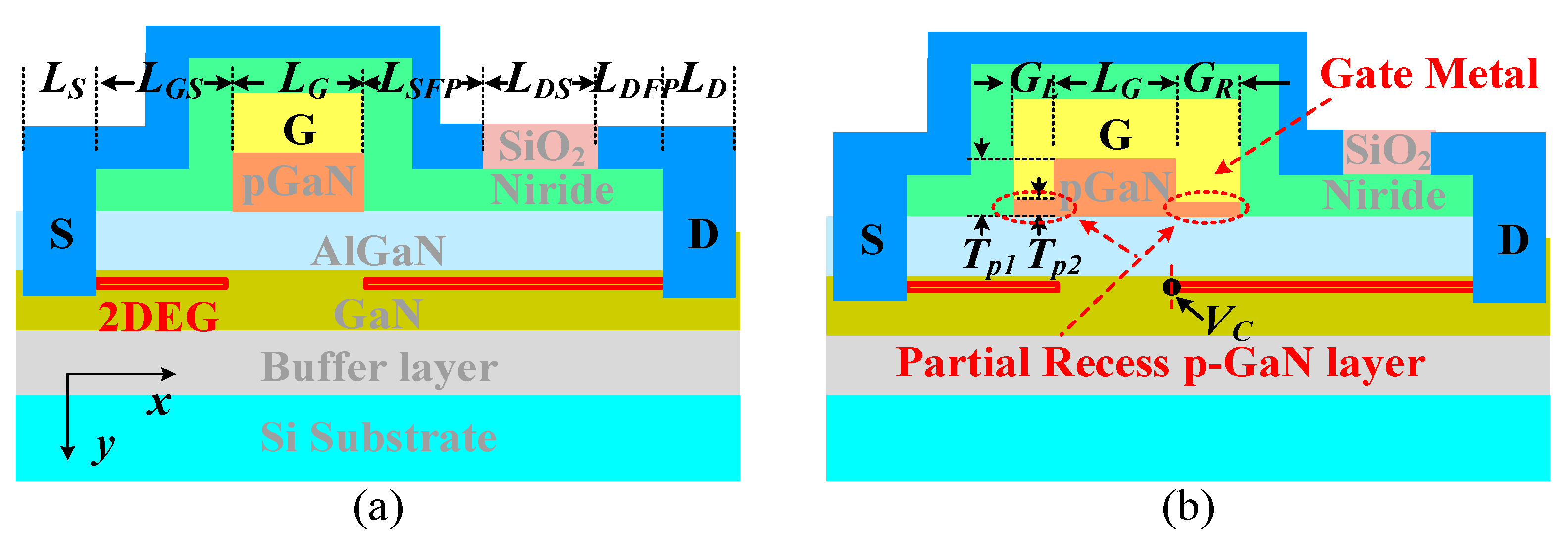
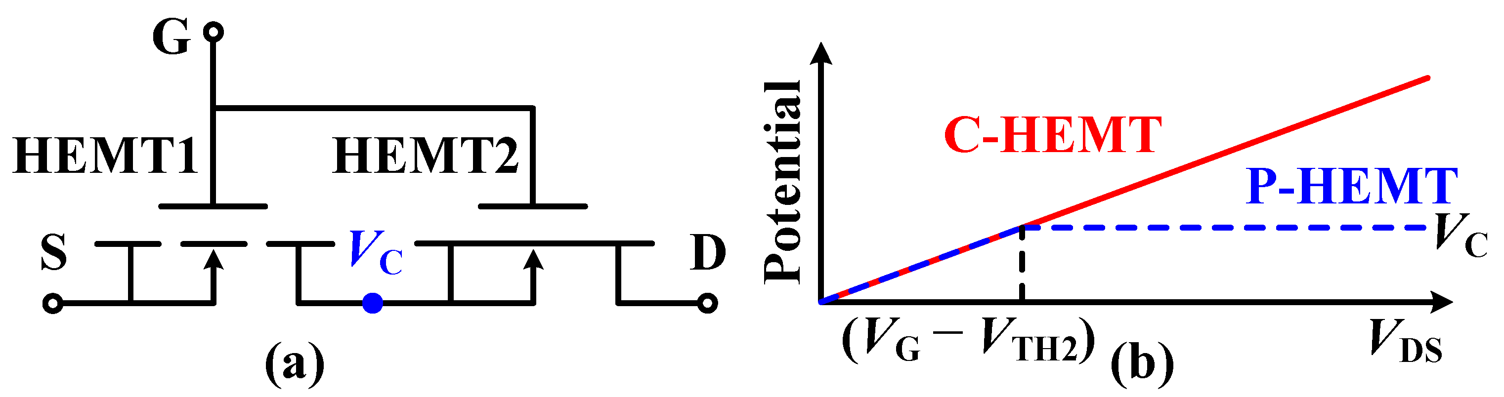
2. Device Structure and Mechanism

The schematic structure of the proposed p-GaN HEMT (P-HEMT) is shown in Figure 1b. Compared with conventional p-GaN HEMT (C-HEMT), the P-HEMT features a partially recessed layer (PR p-GaN layer). To illustrate the mechanism of improving BV and VTH stability for the P-HEMT, we employ one equivalent model with two series HEMTs, which are defined as high threshold voltage HEMT1 and low threshold voltage HEMT2, as shown in Figure 2a. As the threshold voltage of HEMT1 (VTH1) is larger than the threshold voltage of HEMT2 (VTH2), HEMT2 has been turned on when the gate to source voltage (VGS) is larger than VTH1. Therefore, the threshold voltage VTH of P-HEMT is mainly determined by VTH1, namely, VTHVTH1. The potential is defined as VC at the connection node, which is also shown in Figure 1b. When 0 < VC < VGSVTH2 (i.e., VGSVC > VTH2), HEMT2 is at on-state. Therefore, VC increases with VDS at low drain bias. When VC > VGSVTH2 (i.e., VGSVC < VTH2), HEMT2 is in an off-state and the 2DEG channel under the PR p-GaN layer is depleted to withstand VDS voltage. Therefore, VC is clamped and does not increase with VDS at high drain bias, as the blue dash line shown in Figure 2b. As a result, the barrier height for electrons injecting from source to drain will be hardly influenced by high drain bias, which makes VTH more stable. In addition, the stable barrier height leads to decreased electrons flowing from source to drain compared with C-HEMT at high drain bias, which induces delayed occurrence of avalanche breakdown, namely, improves breakdown voltage.

3. Results and Discussions

In this section, the current-voltage and capacitance-voltage characteristics of P-HEMT are investigated by Sentaurus TCAD simulation software [16], and the design considerations are also discussed. In the simulation, the optimized device parameters are as listed in Table 1 unless otherwise specified, which is also based on our previous calibrated work [17]. In particular, the structure parameters of C-HEMT are designed according to the dissected cross-sectional scanning electron microscope (SEM) images. The x- and y-coordinates and the epitaxial structures of the two devices are illustrated in Figure 1 [18]. For C-HEMT, an ionized acceptor concentration Np-GaN = 3.5 × 1017 cm−3 is induced in the p-GaN layer with the tp-GaN = 50 nm, which contributes to VTH and on-state current calibrations for the C-HEMT. In addition, the deep acceptor traps and self-compensating donor traps [19] are also considered in the AlGaN buffer layer with an activation energy of EV + 0.9 eV and EC—0.11 eV [20], and the trap density is 3 × 1016 cm−3 and 1.3 × 1015 cm−3 respectively [21]. Typically, the GL of the PR layer on the source side is only set to 0.1 μm considering the deviation of the fabrication process, and it should be as small as possible to reduce the negative influence on input capacitance in practical application. The GR of the PR layer on the drain side is an adjustable parameter as it makes obvious significance on the improvement of BV and VTH stability. In this paper, the gate length LG of C-HEMT is the same as the length of the thicker p-GaN layer of P-HEMT for achieving the same on-resistance, and the length of the partially-recessed p-GaN layer is not included in the nominal gate length LG. Table 1 shows the calibrated results of the 100 V enhancement-mode p-GaN HEMT [22], and it can be seen that the results are in good agreement with the datasheet as shown in Figure 3. Typically, the BV characteristic considering the avalanche model [23] coincides well with the testing result.

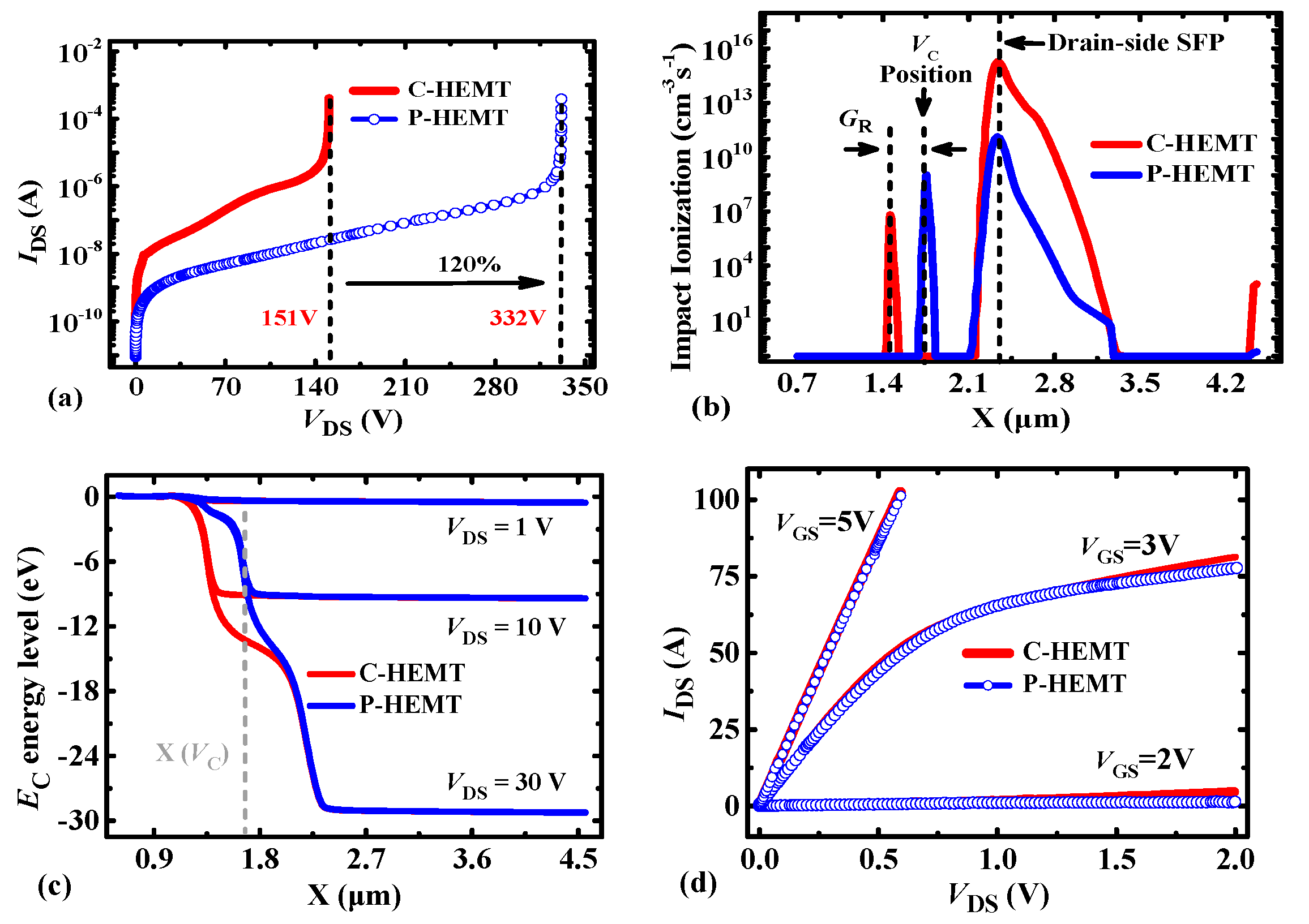
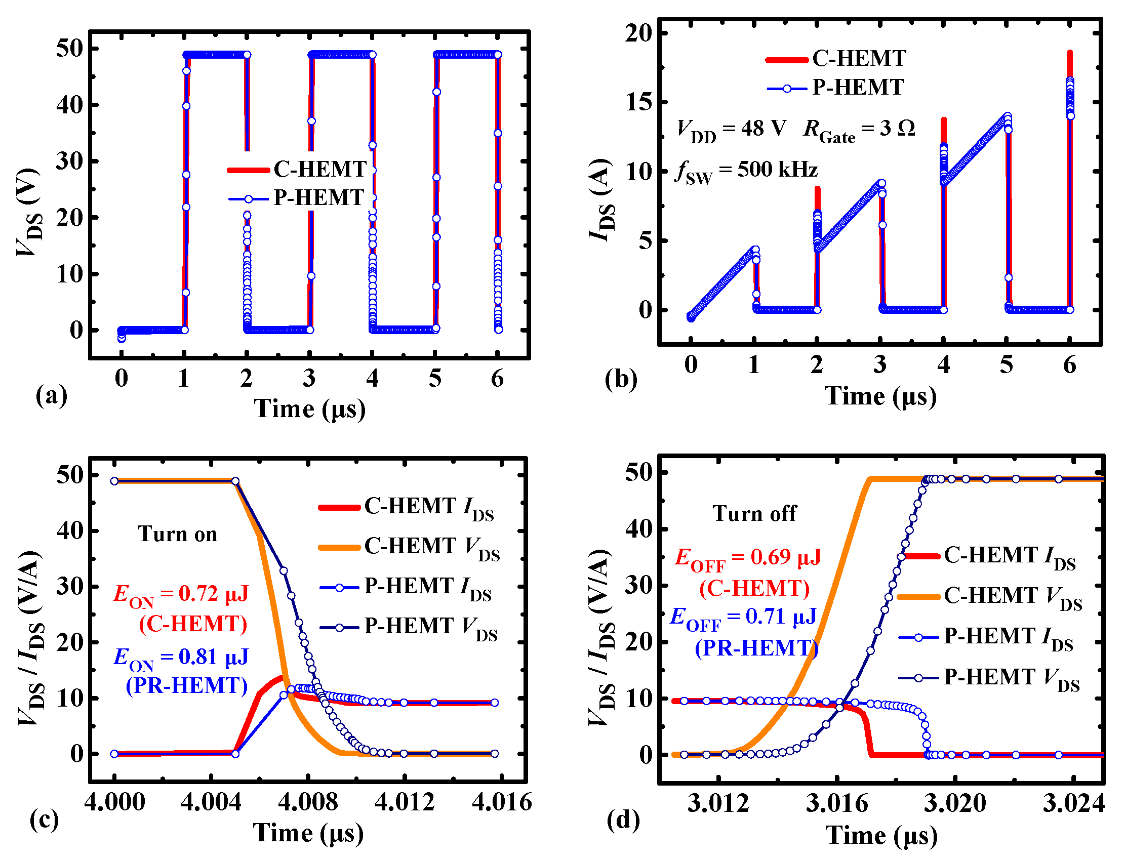
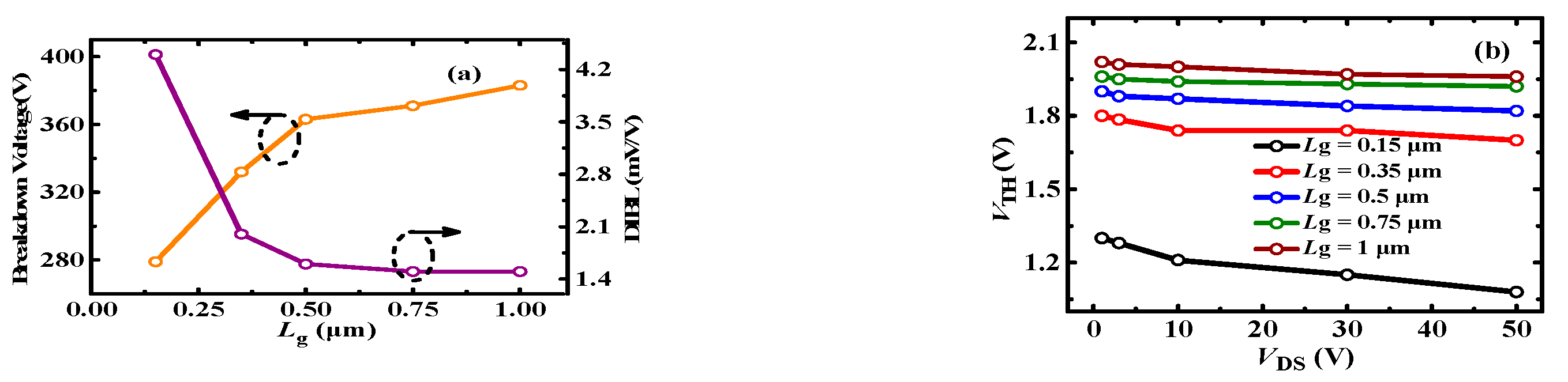
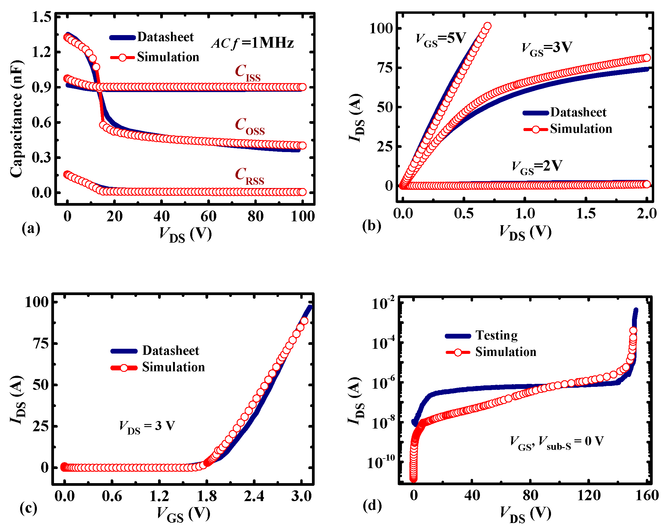
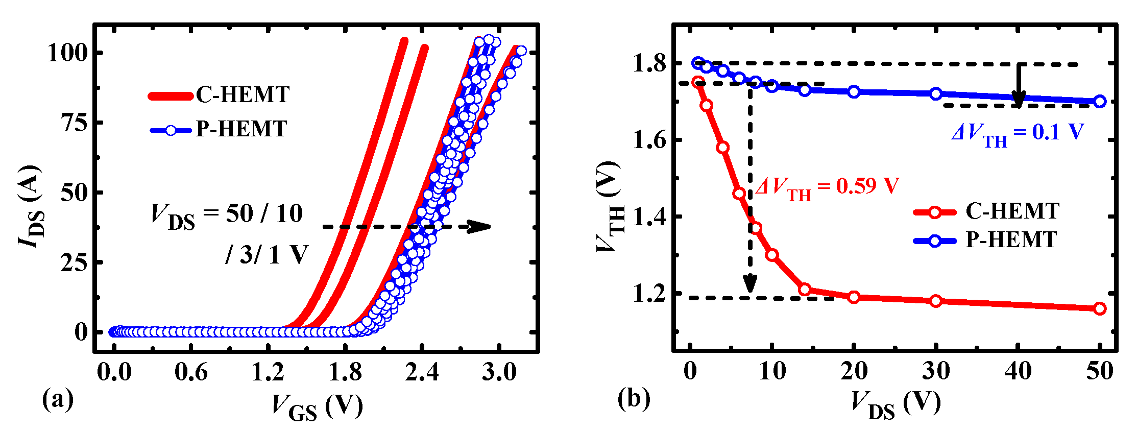
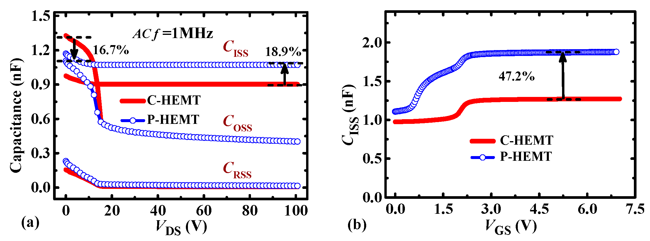
3.1. Static and Transient Characteristics

Figure 4 shows the forward-blocking and output characteristics of the P-HEMT. As shown in Figure 4a, it can be seen that the BV (IDS_off = 100 μA) for the P-HEMT is increased by 120% compared with the 100 V C-HEMT, which mainly results from the delayed occurrence of avalanche breakdown. As shown in Figure 4b, it can be observed that impact ionization at the drain-side source field plate is decreased at the same 150 V drain bias, which results from the decreased electrons flowing from source to drain. In addition, as shown in Figure 4c, the conduction energy EC level at the drain-side of the p-GaN layer for P-HEMT is clamped, which results from the clamped VC as stated in section II. As shown in Figure 4d, for typical gate operation voltage VGS = 5 V, the output curves of C-HEMT and P-HEMT are coincident well, which indicates that the PR p-GaN layer makes a negligible impact on the on-state resistance. For VGS = 2 V, the IDS for C-HEMT is slightly higher than P-HEMT, which results from the partial depletion of the 2DEG channel under the PR p-GaN layer.
Figure 5 shows the transfer characteristics of the P-HEMT. At low drain bias (such as VDS = 1 V), the transfer curves of C-HEMT and P-HEMT are coincident well and the threshold voltage difference is less than 0.05 V. However, with the increasing of VDS, the VTH of C-HEMT decreases obviously while VTH of P-HEMT slightly reduced. Typically, the VTH decrease from VDS = 1 V to VDS = 50 V is 0.59 V for C-HEMT and 0.1 V for P-HEMT, as shown in Figure 5b. The significantly decreased VTH for C-HEMT will lead to false turn-on at high drain bias (typically, from off-state to on-state), which is not acceptable for practical application. However, from the results, it can be deduced that the P-HEMT with more stable VTH can be contributed to alleviating this problem very well.
To illustrate the impact of the PR p-GaN layer on transient behavior, the simulation using a double pulse circuit is carried out, as shown in Figure 6. Compared with C-HEMT, the calculated turn-on loss and turn-off loss of P-HEMT are increased by 0.09 μJ and 0.02 μJ at 500 kHz respectively, and the total switching loss is increased by less than 7.8%. It can be inferred the increased switching loss mainly results from the increase of the input capacitance CISS. As shown in Figure 7, it can be seen that the off-state and on-state input capacitance CISS is increased by 18.9% and 47.2%, respectively. In addition, as shown in Figure 7a, the COSS at high-drain bias (VDS > 15 V) is the same as C-HEMT, and the output capacitance COSS at a low-drain bias (VDS < 15 V) is decreased by 16.7%, which mainly results from the depletion of 2DEG channel under the PR layer as stated in section II. The decrease of COSS at VDS < 15 V is contributed to reducing the increment of switching loss.

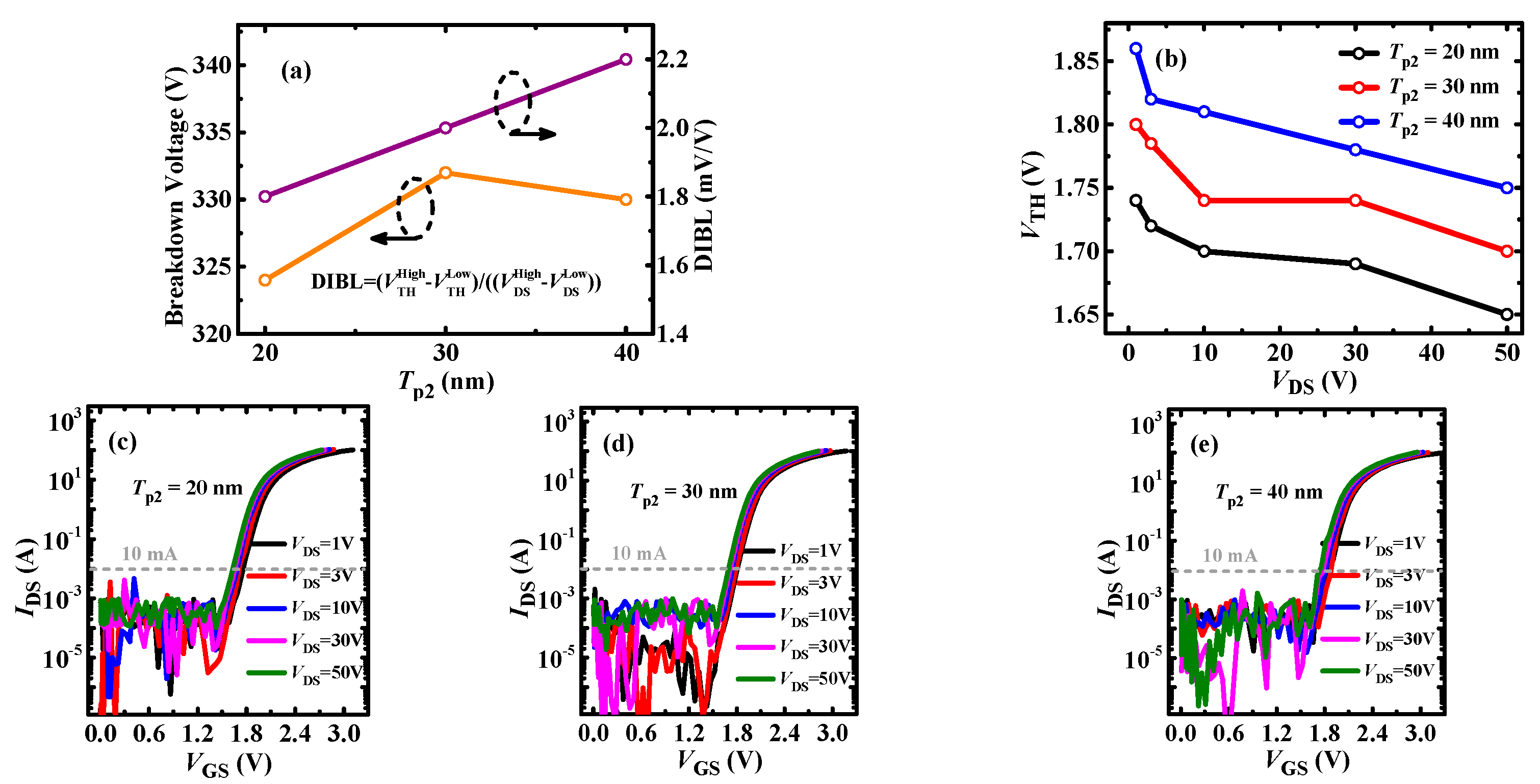
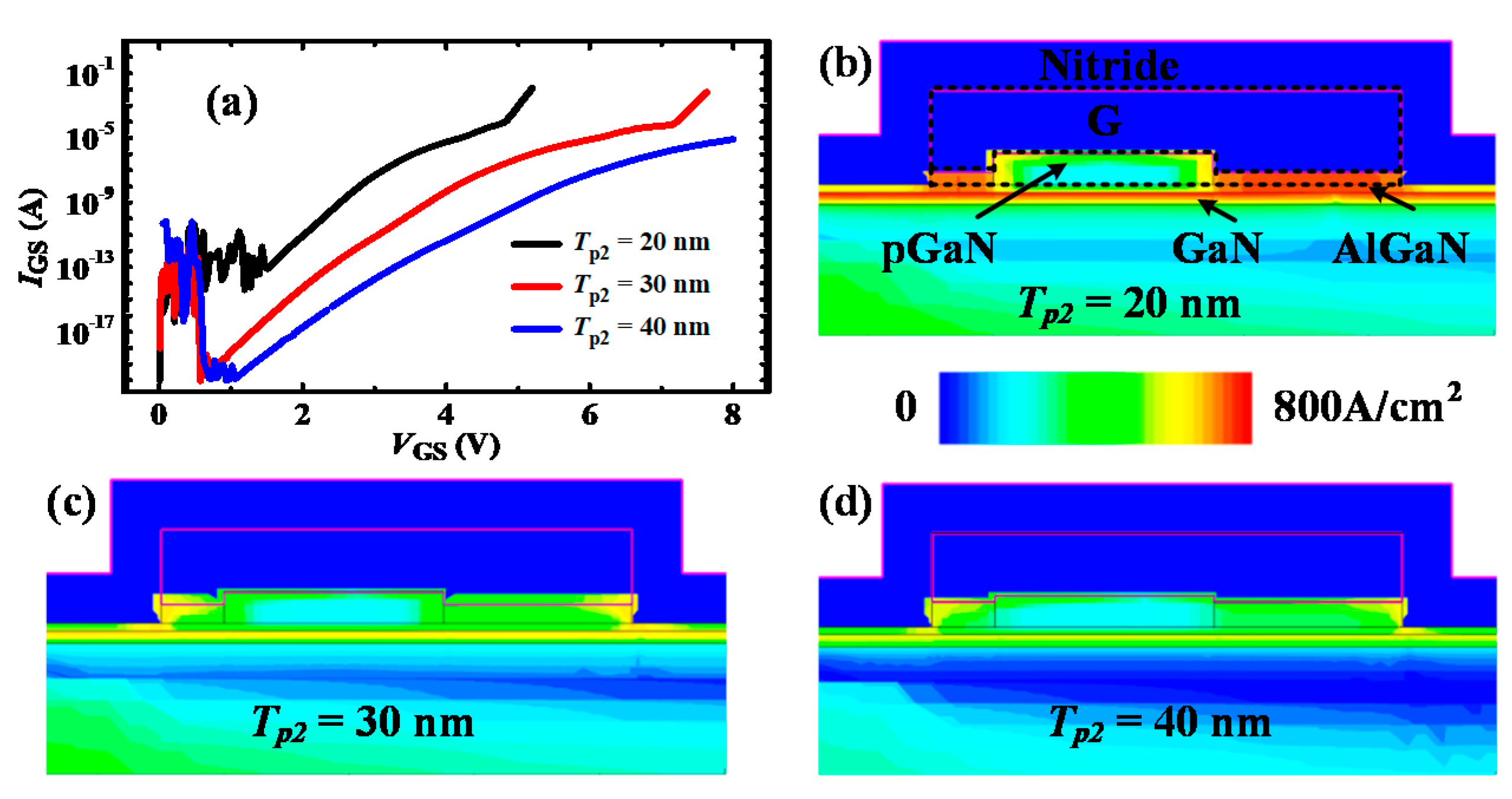
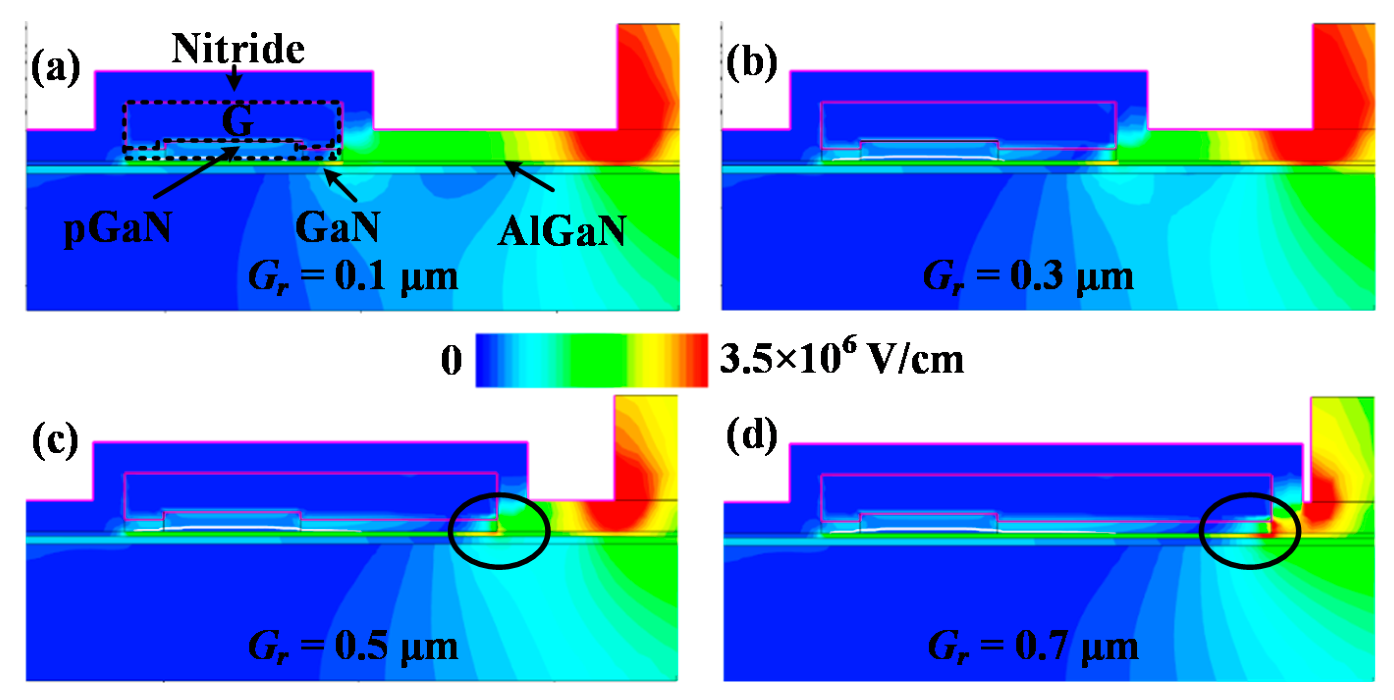
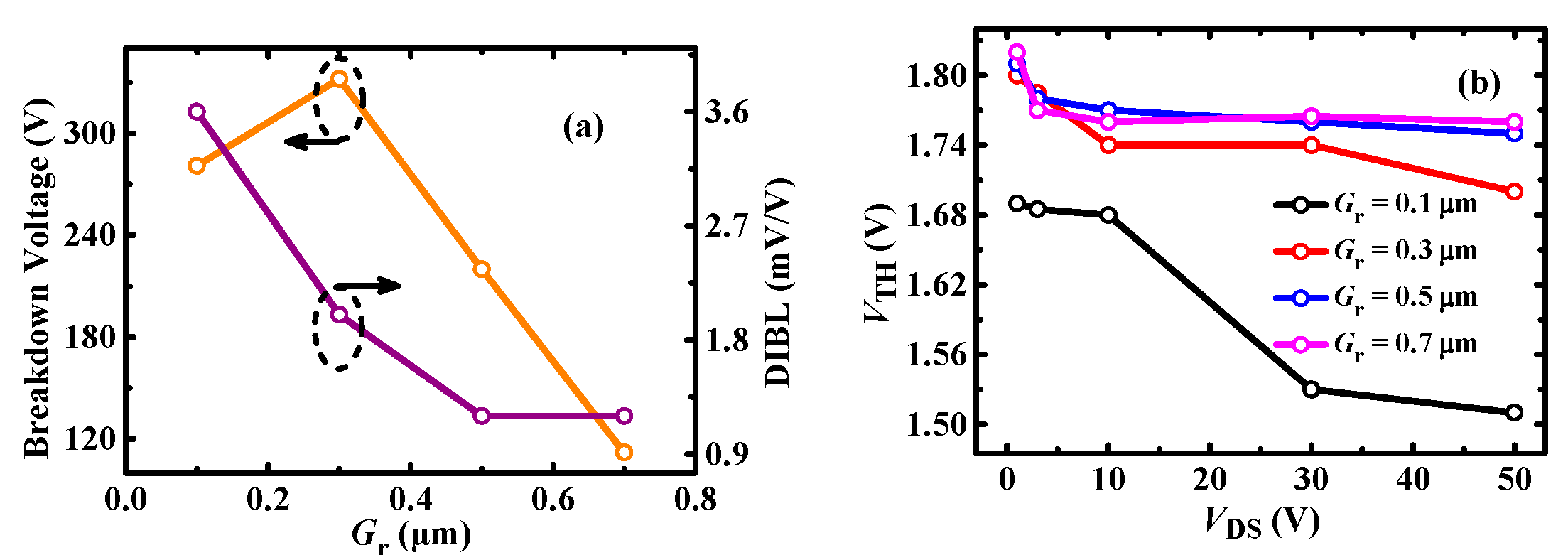
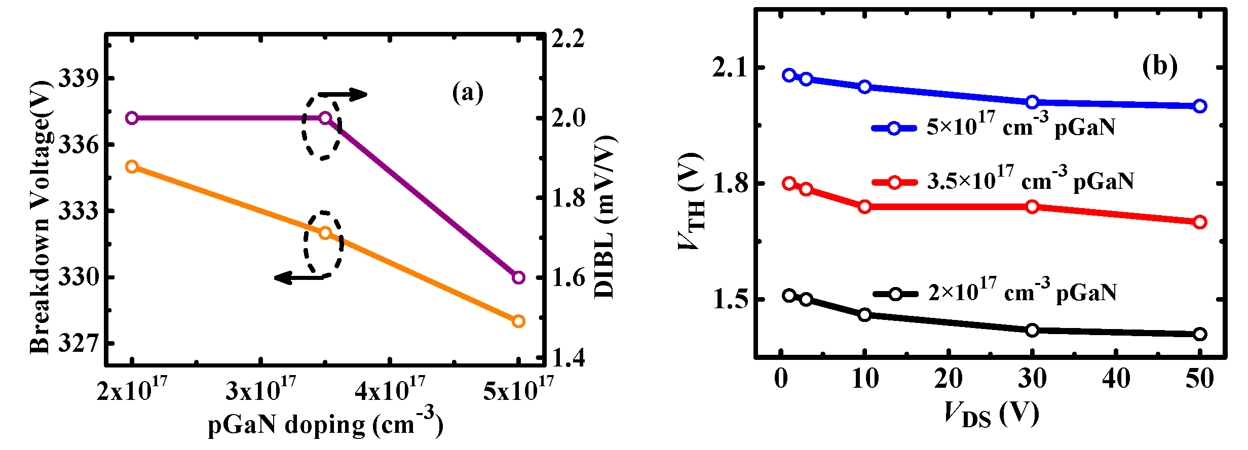
3.2. Design Considerations of P-HEMT

This section mainly discusses the impact of PR p-GaN layers’ thickness, length, and doping concentration on the BV and VTH stability.
Figure 8 shows the VTH and BV results for different thicknesses of the PR p-GaN layer. As shown in Figure 8a, it can be seen that the DIBL value is increased with PR p-GaN layer thickness. The DIBL parameter is defined as ( V T H H i g h V T H L o w )/( V D S H i g h V D S L o w ) to represent the VTH stability, and the smaller value symbolizes the more stable VTH. As shown in Figure 8b, it can be seen that the VTH for different thickness PR layers from VDS = 1 V to VDS = 50 V decreases, but the difference is all less than 0.1 V, which indicates the high stable VTH for P-HEMT. The log-scale transfer characteristics are as shown in Figure 8c–e. For the same drain bias, the VTH slightly increases (≤0.05 V) with the thickness of the PR p-GaN layer, which mainly results from the 2DEG depletion under the PR p-GaN layer. In addition, it can be observed that the BV is all larger than 320 V, which indicates the impact of the PR p-GaN layer’s thickness on BV is negligible. However, for a smaller thickness PR p-GaN layer, the gate-to-source breakdown voltage can be reduced. Figure 9a shows the IGSVGS characteristics for 20/30/40 nm PR p-GaN layer, and it can be seen that the IGS for Tp2 = 20 nm abruptly increases when VGS is larger than 5.1 V. To explore the origin of the abrupt IGS, the current distribution of the three thickness PR p-GaN layer devices are plotted, as shown in Figure 9b–d. For the device with Tp2 = 20 nm, the current density from the PR p-GaN layer to the 2DEG channel is larger than the normal thickness p-GaN layer. This indicates the high gate current mainly results from the breakdown of the PR p-GaN layer. As a comparison, the gate current density for Tp2 = 30/40 nm is very small. Based on the above analysis, it can be deduced that the PR p-GaN layer thickness should be taken into careful consideration in the design to avoid gate breakdown.
Figure 10 shows the impact of PR p-GaN layer length on the BV and VTH characteristics. It can be seen that DIBL decreases with Gr, which indicates the VTH stability is increased. However, the DIBL tends to be stable and the BV decreases when Gr is larger than 0.5 μm. The decrease of the BV mainly results from the high electric field at the drain-side of the PR p-GaN layer, as shown in Figure 11. Therefore, it can be deduced that the PR p-GaN layer length should be in a reasonable range to get a good trade-off for VTH stability and high BV. For the 100 V p-GaN HEMT discussed in this paper, the 0.3~0.5 μm PR p-GaN layer is recommended.
Figure 12 shows the impact of p-GaN doping density on the VTH and BV. It can be observed that the p-GaN doping density mainly determines the magnitude of VTH, and it makes a negligible effect on BV and DIBL. Figure 13 shows the VTH and BV characteristics of P-HEMT with different gate lengths Lg. It can be seen that longer gate length induces higher VTH, lower DIBL, which means longer gate length is contributed to making VTH more stable. In addition, longer gate length induces higher BV, which mainly results from the electric field modulation. However, longer gate length will induce higher on-resistance. Therefore, the gate length should be taken into careful consideration to get a better trade-off for VTH stability, BV, and RON.

4. Conclusions

This paper proposes a novel p-GaN HEMT with a PR p-GaN layer to improve BV and VTH stability. The device features a PR p-GaN layer compared with conventional p-GaN HEMT. At high drain bias, the two-dimensional electron gas channel under the PR p-GaN layer is depleted to withstand VDS, thereby contributing to improving the BV and VTH stability. Compared with the C-HEMT, simulation results show that the breakdown voltage is improved by 120%, and the VTH stability changing with VDS is increased by 490% (the decrease of VTH at 50 V for P-HEMT and C-HEMT are 0.1 V and 0.59 V respectively). The static transfer and output characteristics are the same as the C-HEMT, and the total switching loss at 500 kHz is increased less than 7.8%. In addition, we investigated the impact of the PR layers’ length, thickness, doping density on the performance.

Author Contributions

Methodology, H.W.; investigation, H.W., Y.S., Y.X., and C.L.; writing—review and editing, Y.S., and Y.X.; supervision, G.L.; project administration, Y.H. All authors have read and agreed to the published version of the manuscript.

Funding

This work was supported by the National Key R&D Program of China (No. 2020YFF0218503).

Institutional Review Board Statement

Not applicable.

Informed Consent Statement

Not applicable.

Data Availability Statement

Not applicable.

Conflicts of Interest

The authors declare no conflict of interest. The funders had no role in the design of the study; in the collection, analyses, or interpretation of data; in the writing of the manuscript, or in the decision to publish the results.

References

  1. Chen, W.; Wong, K.-Y.; Chen, K.J. Single-Chip Boost Converter Using Monolithically Integrated AlGaN/GaN Lateral Field-Effect Rectifier and Normally Off HEMT. IEEE Electron Device Lett. 2009, 30, 430–432. [Google Scholar] [CrossRef]
  2. Meneghini, M.; Cibin, G.; Bertin, M.; Hurkx, G.A.M.; Ivo, P.; Šonský, J.; Croon, J.A.; Meneghesso, G.; Zanoni, E. OFF-state degradation of AlGaN/GaN power HEMTs: Experimental demonstration of time-dependent drain-source breakdown. IEEE Trans. Electron Devices 2014, 61, 1987–1992. [Google Scholar] [CrossRef]
  3. Meneghini, M.; Hilt, O.; Fleury, C.; Silvestri, R.; Capriotti, M.; Strasser, G.; Pogany, D.; Bahat-Treidel, E.; Brunner, F.; Knauer, A. Normally-off GaN-HEMTs with p-type gate: Off-state degradation, forward gate stress and ESD failure. Microelectron. Reliab. 2016, 58, 177–184. [Google Scholar] [CrossRef]
  4. Wang, H.; Wei, J.; Xie, R.; Liu, C.; Tang, G.; Chen, K.J. Maximizing the performance of 650-V p-GaN gate HEMTs: Dynamic RON characterization and circuit design considerations. IEEE Trans. Power Electron. 2016, 32, 5539–5549. [Google Scholar] [CrossRef]
  5. Ishida, H.; Kajitani, R.; Kinoshita, Y.; Umeda, H.; Ujita, S.; Ogawa, M.; Tanaka, K.; Morita, T.; Tamura, S.; Ishida, M.; et al. GaN-based Semiconductor Devices for Future Power Switching Systems. In Proceedings of the 2016 IEEE International Electron Devices Meeting (IEDM), San Francisco, CA, USA, 3–7 December 2016. [Google Scholar]
  6. Chen, K.J.; Häberlen, O.; Lidow, A.; Tsai, C.L.; Ueda, T.; Uemoto, Y.; Wu, Y. GaN-on-Si power technology: Devices and applications. IEEE Trans. Electron Devices 2017, 64, 779–795. [Google Scholar] [CrossRef]
  7. Kim, J.G.; Cho, C.; Kim, E.; Hwang, J.S.; Park, K.H.; Lee, J.H. High Breakdown Voltage and Low-Current Dispersion in AlGaN/GaN HEMTs with High-Quality AlN Buffer Layer. IEEE Trans. Electron Devices 2021, 68, 1513–1517. [Google Scholar] [CrossRef]
  8. Duan, B.; Yang, L.; Wang, Y.; Yang, Y. Experimental Results for AlGaN/GaN HEMTs Improving Breakdown Voltage and Output Current by Electric Field Modulation. IEEE Trans. Electron Devices 2021, 68, 2240–2245. [Google Scholar] [CrossRef]
  9. Xin, Y.; Chen, W.; Sun, R.; Shi, Y.; Liu, C.; Xia, Y.; Wang, F.; Li, M.L.J.; Zhou, Q.; Deng, X.; et al. Analytical Switching Loss Model for GaN-Based Control Switch and Synchronous Rectifier in Low-Voltage Buck Converters. IEEE J. Emerg. Sel. Top. Power Electron. 2019, 7, 1485–1495. [Google Scholar] [CrossRef]
  10. Zhao, X.; Xu, Y.; Jia, Y.; Wu, Y.; Xu, R.; Li, J.; Hu, Z.; Wu, H.; Dai, W.; Cai, S. Temperature-Dependent Access Resistances in Large-Signal Modeling of Millimeter-Wave AlGaN/GaN HEMTs. IEEE Trans. Microw. Theory Tech. 2017, 65, 2271–2278. [Google Scholar] [CrossRef]
  11. Das, S.; Kundu, S. Simulation to Study the Effect of Oxide Thickness and High-K Dielectric on Drain-Induced Barrier Lowering in N-type MOSFET. IEEE Trans. Nanotechnol. 2013, 12, 945–947. [Google Scholar] [CrossRef]
  12. Park, P.S.; Rajan, S. Simulation of Short-Channel Effects in N- and Ga-Polar AlGaN/GaN HEMTs. IEEE Trans. Electron Devices 2011, 58, 704–708. [Google Scholar] [CrossRef]
  13. Singisetti, U.; Wong, M.H.; Dasgupta, S.; Swenson, B.; Thibeault, B.J.; Speck, J.S.; Mishra, U.K. Enhancement-Mode N-Polar GaN MISFETs with Self-Aligned Source/Drain Regrowth. IEEE Electron Device Lett. 2011, 32, 137–139. [Google Scholar] [CrossRef]
  14. Pinchbeck, J.; Lee, K.B.; Jiang, S.; Houston, P. Dual metal gate AlGaN/GaN high electron mobility transistors with improved transconductance and reduced short channel effects. J. Phys. D Appl. Phys. 2021, 54, 105104. [Google Scholar] [CrossRef]
  15. Lu, B.; Saadat, O.I.; Palacios, T. High-Performance Integrated Dual-Gate AlGaN/GaN Enhancement-Mode Transistor. IEEE Electron Device Lett. 2010, 31, 990–992. [Google Scholar] [CrossRef]
  16. Synopsys. TCAD Sentaurus™ Tutorial. Available online: http://www.sentaurus.dsod.pl/index.html (accessed on 19 January 2022).
  17. Wang, F.; Chen, W.; Xu, X.; Sun, R.; Wang, Z.; Xia, Y.; Xin, Y.; Liu, C.; Zhou, Q.; Zhang, B. Simulation Study of an Ultralow Switching Loss p-GaN Gate HEMT With Dynamic Charge Storage Mechanism. IEEE Trans. Electron Devices 2021, 68, 175–183. [Google Scholar] [CrossRef]
  18. Lidow, A.; de Rooij, M.; Strydom, J.; Reusch, D.; Glaser, J. GaN Transistors for Efficient Power Conversion; John Wiley & Sons: Hoboken, NJ, USA, 2019. [Google Scholar]
  19. Joshi, V.; Tiwari, S.P.; Shrivastava, M. Part I: Physical Insight Into Carbon-Doping-Induced Delayed Avalanche Action in GaN Buffer in AlGaN/GaN HEMTs. IEEE Trans. Electron Devices 2019, 66, 561–569. [Google Scholar] [CrossRef]
  20. Verzellesi, G.; Morassi, L.; Meneghesso, G.; Meneghini, M.; Zanoni, E.; Pozzovivo, G.; Lavanga, S.; Detzel, T.; Häberlen, O.; Curatola, G. Influence of Buffer Carbon Doping on Pulse and AC Behavior of Insulated-Gate Field-Plated Power AlGaN/GaN HEMTs. IEEE Electron Device Lett. 2014, 35, 443–445. [Google Scholar] [CrossRef]
  21. Chini, A.; Meneghesso, G.; Meneghini, M.; Fantini, F.; Verzellesi, G.; Patti, A.; Iucolano, F. Experimental and Numerical Analysis of Hole Emission Process From Carbon-Related Traps in GaN Buffer Layers. IEEE Trans. Electron Devices 2016, 63, 3473–3478. [Google Scholar] [CrossRef]
  22. EPC. eGaN FET Datasheet. Available online: https://epc-co.com/epc/Portals/0/epc/documents/datasheets/epc2001_datasheet.pdf (accessed on 19 January 2022).
  23. Cheng, Y.; Wang, Y.; Feng, S.; Zheng, Z.; Chen, K.J. Observation and characterization of impact ionization-induced OFF-state breakdown in Schottky-type p-GaN gate HEMTs. Appl. Phys. Lett. 2021, 118, 163502. [Google Scholar] [CrossRef]
  24. Wang, F.; Chen, W.; Li, X.; Sun, R.; Zhang, B. Charge storage impact on input capacitance in p-GaN gate AlGaN/GaN power high-electron-mobility transistors. J. Phys. D Appl. Phys. 2020, 53, 305106. [Google Scholar] [CrossRef]
Figure 1. The schematic device structures of (a) conventional p-GaN HEMT (C-HEMT) and (b) proposed p-GaN HEMT (P-HEMT) with partially-recessed p-GaN layer (PR p-GaN layer).
Micromachines 13 00176 g001
Figure 2. (a) The equivalent model of the P-HEMT with a high threshold voltage HEMT1 and a low threshold voltage HEMT2; (b) the potential VC versus VDS.
Micromachines 13 00176 g002
Figure 3. (a) Capacitance-Voltage characteristic; (b) output characteristic; (c) transfer characteristic; (d) forward-blocking characteristic. The forward-blocking characteristic is based on the testing data as there is no breakdown voltage result in the datasheet.
Micromachines 13 00176 g003
Figure 4. Comparison of the (a) forward-blocking characteristic, (b) impact ionization profile along the channel at VDS = 150 V, (c) conduction energy level EC profile along the channel, and (d) output characteristic between C-HEMT and P-HEMT.
Micromachines 13 00176 g004
Figure 5. Comparison of (a) the transfer, (b) the threshold voltage VTH (at IDS = 10 mA) depending on VDS between the C-HEMT and P-HEMT. For a fair comparison, the VTH is defined when IDS =10 mA.
Micromachines 13 00176 g005
Figure 6. The switching transient comparison between C-HEMT and P-HEMT by double-pulse simulation. (a) VDS voltage waveforms; (b) IDS current waveforms; (c) turn on transient at ~10 A IDS current; (d) turn off transient at ~10 A IDS current.
Micromachines 13 00176 g006
Figure 7. Comparison of (a) capacitance-VDS, and (b) CISS-VGS characteristics between C-HEMT and P-HEMT.
Micromachines 13 00176 g007
Figure 8. (a) Breakdown voltage (BV) and DIBL versus PR thickness; (b) the threshold voltage VTH (at IDS = 10 mA) depending on VDS; the transfer characteristics of P-HEMT with Tp2 = (c) 20 nm; (d) 30 nm; (e) 40 nm.
Micromachines 13 00176 g008
Figure 9. (a) The IGS-VGS characteristics of P-HEMT with different Tp2; the current distribution at the gate part for Tp2 = (b) 20 nm, (c) 30 nm, (d) 40 nm.
Micromachines 13 00176 g009
Figure 10. (a) BV and DIBL, (b) VTH (at IDS = 10 mA) depending on VDS for different Gr length.
Micromachines 13 00176 g010
Figure 11. The electric field distribution of P-HEMT for Gr = (a) 0.1 μm; (b) 0.3 μm; (c) 0.5 μm; (d) 0.7 μm at breakdown voltage.
Micromachines 13 00176 g011
Figure 12. (a) BV and DIBL, (b) VTH (at IDS = 10 mA) depending on VDS for different p-GaN doping density.
Micromachines 13 00176 g012
Figure 13. (a) BV and DIBL, (b) VTH depending on VDS for different gate lengths.
Micromachines 13 00176 g013
Table 1. Device parameters specification.
SymbolsDefinitionsTypical Value
LSSource length0.7 μm
LGGate length0.35 μm
LDSource-to-gate length0.7 μm
LGSSource-to-gate length0.4 μm
LDS-CC-HEMT Gate-to-drain length1.95 μm
LDS-PRP-HEMT Gate-to-drain length1.95 μm
LSFP-CC-HEMT Source-field-plate length0.8 μm
LSF-PRP-HEMT Source-field-plate length(0.8—Gr) μm
LDFPDrain-field-plate length0.25 μm
tSiNThickness of SiN80 nm
tSiO2Thickness of SiO2270 nm
GLThe left PR p-GaN length0.1 μm
GRThe right PR p-GaN length0.3 μm
Tp2Thickness of PR p-GaN30 nm
Tp1Thickness of p-GaN50 nm
tbaThickness of barrier12.5 nm
tchThickness of channel20 nm
tbuThickness of buffer2 μm
tnuThickness of nucleation10 nm
tsubThickness of substrate550 μm
tgateThickness of Schottky gate100 nm
χbaAl composition of barrier25%
χbuAl composition of buffer5%
WGWork-function of the gate4.8 eV
NDT1Nitride/AlGaN trap density3 × 1013 cm2 (EC − 0.4 eV) [24]
NDTCChannel UID concentration1 × 1015 cm3
NAT1Buffer acceptor trap density3 × 1016 cm3 (EV + 0.9 eV) [17]
NDT2Buffer donor trap density1.3 × 1015 cm3 (EC − 0.11 eV)
NAT2Silicon/AlN acceptor trap density3 × 1013 cm2 (EC − 1.7 eV)
Np-GaNActivated Mg Doping3.5 × 1017 cm3
Publisher’s Note: MDPI stays neutral with regard to jurisdictional claims in published maps and institutional affiliations.

