1. Introduction
The advancement of portable electronic devices is primarily reliant on wireless data transfer technology. These smart electronic devices may perform a variety of functions, such as sensing, remote access, automation, health monitoring, and so on. Wireless communication needs a large bandwidth ensuring uninterrupted data transfer to take advantage of these features. The ultrawideband (UWB) technology addresses the requirement for increased bandwidth. In UWB, an unlicensed frequency band of 3.1 to 10.6 GHz is designated for commercial use [
1]. The inclusion of the 7.5 GHz bandwidth in the UWB system has gained attention and led to significant advancements in wireless communication systems. The UWB technology communicates via shorter electromagnetic pulses. The UWB antenna design plays a crucial role in the UWB system as it has to meet the precise time and frequency domain characteristics over the impedance bandwidth. The microstrip antenna is very popular due to its ease of installation in front-end radio frequency design. Monopole antennas, in particular, are highly promising for UWB wireless communication because of their advantages of compactness, high bandwidth, and low cost [
2,
3]. The first step in realizing the UWB spectrum is to create a standard rectangular or circular monopole antenna. Adjusting a monopole antenna’s radiating and ground plane structures affects the transmission line characteristics and disrupts the uniform current distribution, resulting in impedance matching over the intended frequency of operation. Various antenna configurations are described in the literature to achieve impedance matching over the UWB band. In [
4], the authors present an inverted L-shape with a microstrip feedline and a square slot antenna. The geometrical adjustment of the feedline and slot contributes to achieving an impedance bandwidth of 3.5 to 9.5 GHz. The combination of different geometrical cylinders with coplanar waveguide (CPW) staircase slot ground structure UWB monopole antenna is demonstrated in [
5]. The rectangular radiator with arc shape truncation at the lower corner and CPW arrangement used to realize the frequency from 3.1–11.8 GHz is presented in [
6]. For the UWB spectrum, an arc-shaped radiator with a lower ground plane composed of parasitic components is illustrated in [
7,
8]. The extended UWB band monopole antenna consisting of a spline-enhanced based radiator and defected ground structure (DGS) is presented in [
9].
Although the UWB system has numerous benefits, including wide bandwidth, it interferes with the existing narrow bands. Conventional antenna design techniques for band rejection characteristics are generally centered on employing a half- or quarter-wavelength filter arrangement. Several other techniques for eliminating single or multiple frequency bands have been reported in the literature, including different structured parasitic elements loading on the radiator and ground plane, metamaterial loading, embedding the filter and antenna, and combining two or more notching techniques as a hybrid approach [
10]. The Sprocket gear wheel-shaped radiating patch defected by the arc and rectangular slots to accomplish two frequency band notches is presented in [
11]. The fractal UWB antenna in [
12] comprises an inverted S and a pair of L-shaped slots and stubs on the radiator to accomplish WLAN and X-band frequency notching. In [
13], the WiMAX and WLAN frequency bands are filtered utilizing S and inverted U structure slots on the hexagonal patch and ground plane. The authors in [
14] illustrate the WLAN and X-band notching characteristics of the circular ring UWB antenna. Band notching is accomplished using parasitic elements on the radiator and a capacitively-loaded loop on the ground plane. The design and positioning of the notching element on the radiator or ground plane primarily influence the desired frequency of notching.
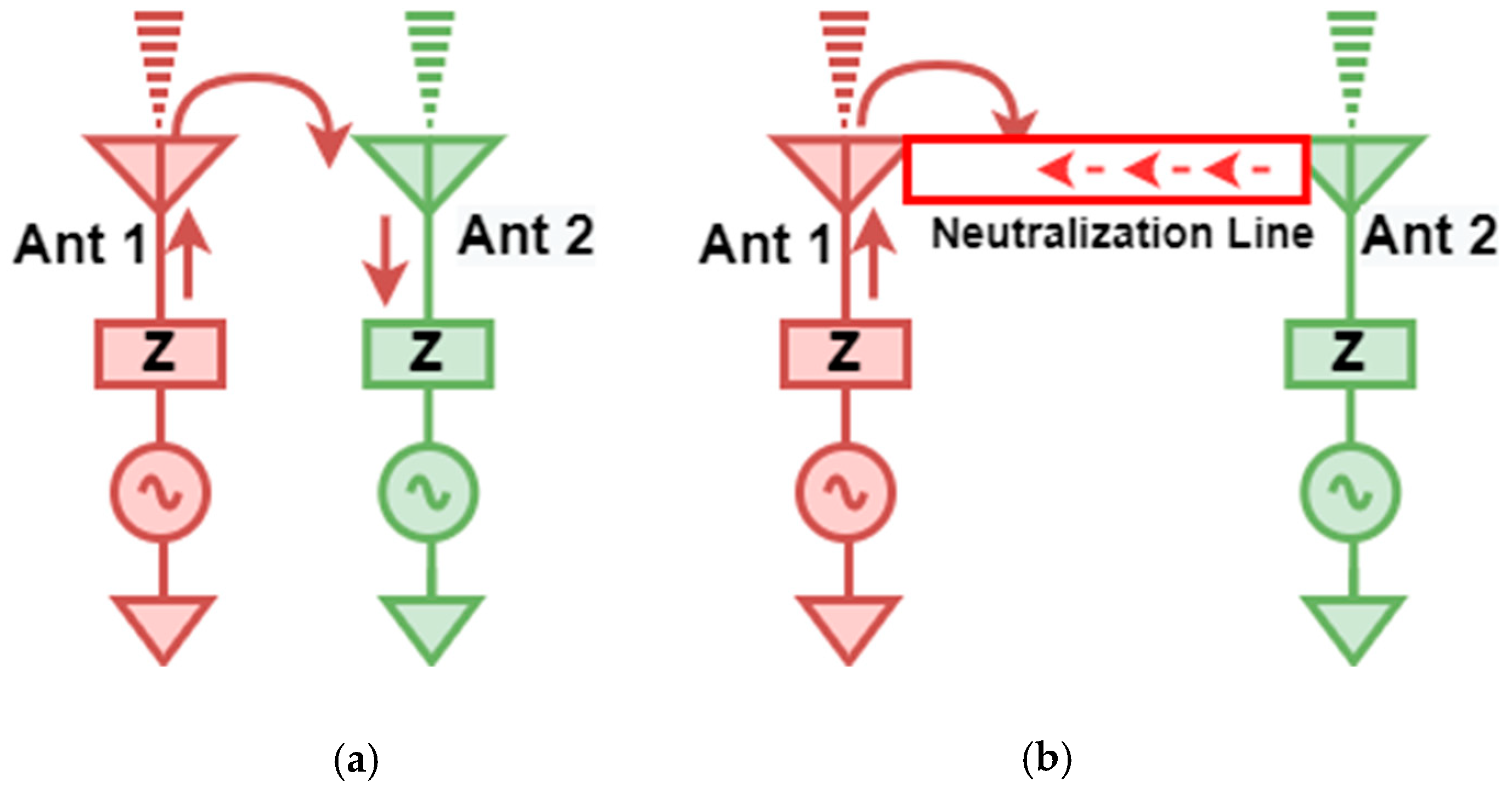
The need for good reproducibility, i.e., wireless links susceptible to multipath fading and higher data rate, is rising proportionally to the progress of wireless communication technology. The portable gadgets are outfitted with diverse approaches to meet the requirement without extending either the spectrum or the transmission power. The compactness features of devices confine the placement and floor planning of the sub-components. Furthermore, putting several antennas in a small area will cause strong mutual coupling between the antennas. In the literature, a large number of band-notched UWB MIMO antennas have already been documented. In such antenna systems, isolation is enhanced by utilizing different approaches, such as defected ground structure (DGS), decoupling networks, neutralization line (NL), metamaterial loading onto the ground and radiator, incorporating filters, and a combination of two or more decoupling structures as hybrid techniques, as reported in [
15,
16]. In [
17], a two-port UWB fractal antenna with the dimensions of 26 × 35 mm
2 operating from 2–10.6 GHz was demonstrated. The presented antenna has dual band notch features at 3.5 GHz and 5.2 GHz by embedding a slot and stub on the radiator. The coupling of the antenna is reduced by introducing the strip on the ground plane. An orthogonally arranged two-port circular monopole UWB antenna with dimensions of 25 × 39 mm
2 is illustrated in [
18]. The presented antenna has dual notches at 5.4 GHz and 7.5 GHz by engraving L-shaped slots onto the radiator. The U-shaped branches entrenched in the ground plane reduce the mutual coupling. The electromagnetic band gap (EBG) structure that separates the two CPW-fed UWB antennas to enhance the isolation (>20 dB) is presented in [
19]. The presented design has dimensions of 35 × 32 mm
2 with the S11 curve ranging from 3.4 GHz to 10.4 GHz.
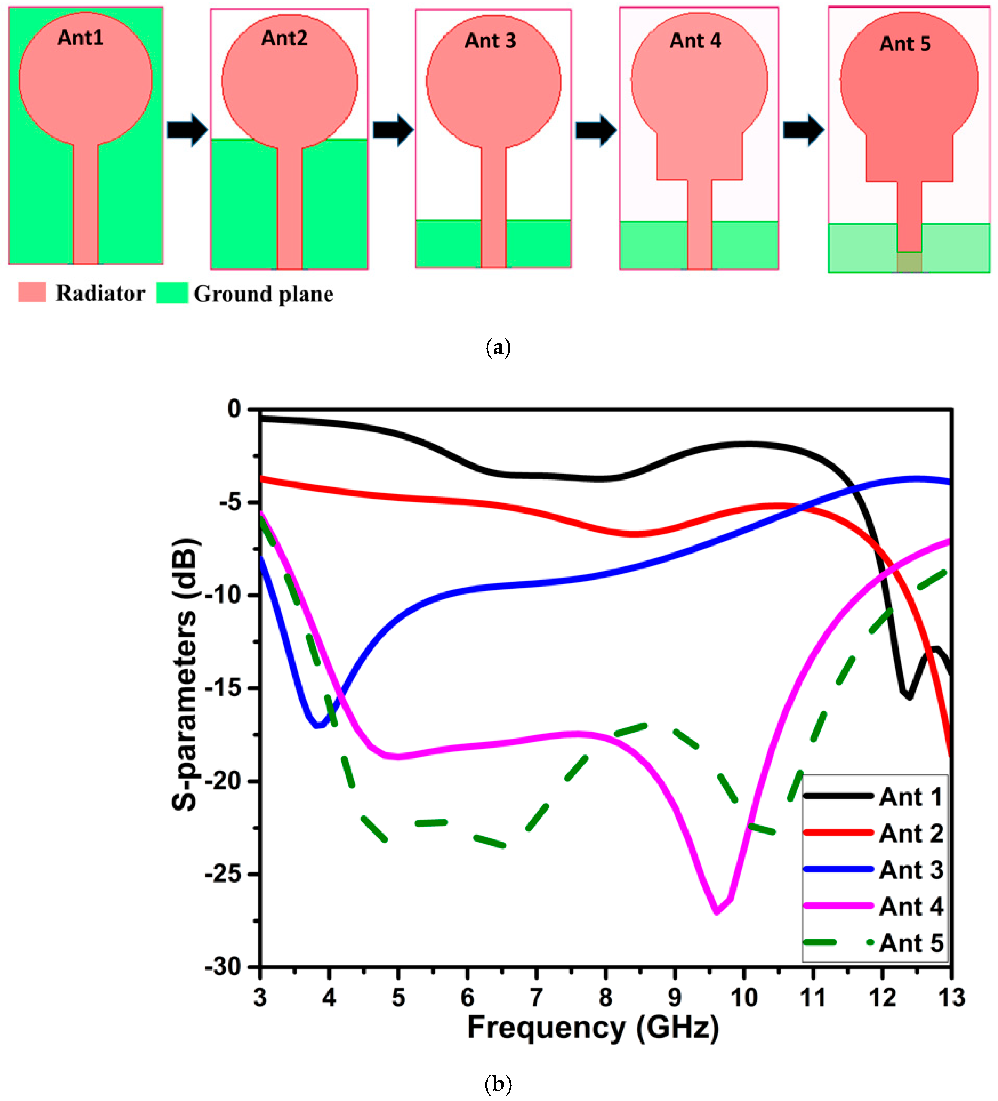
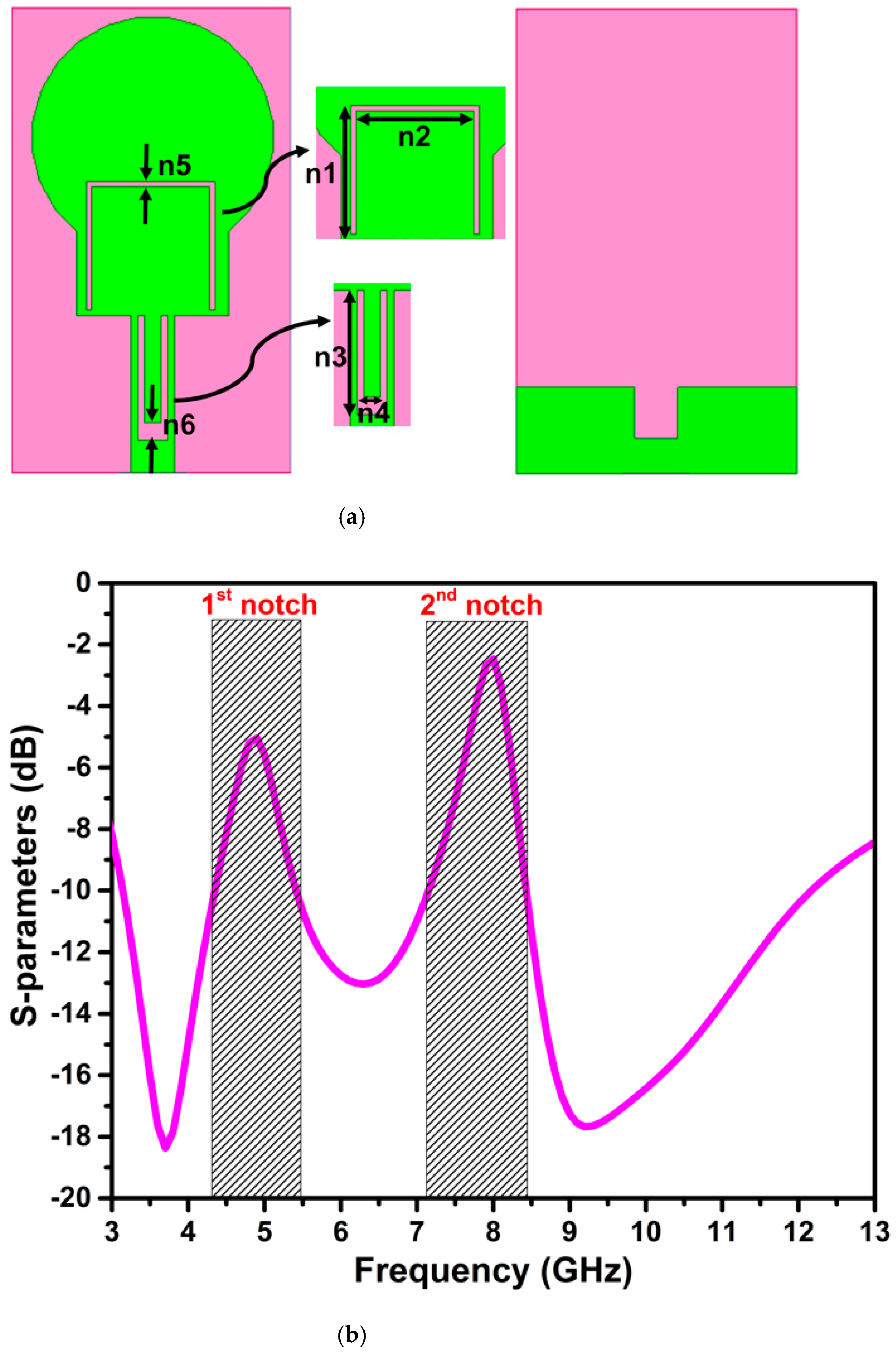
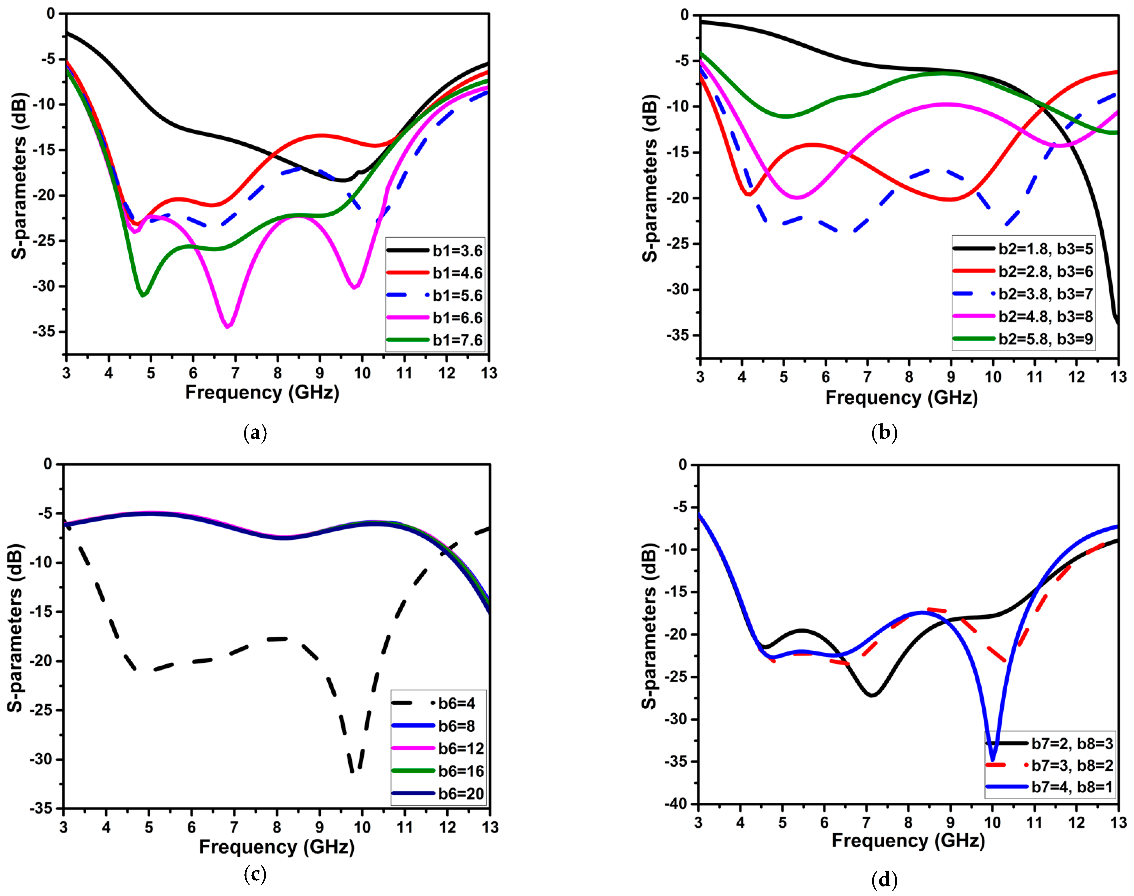
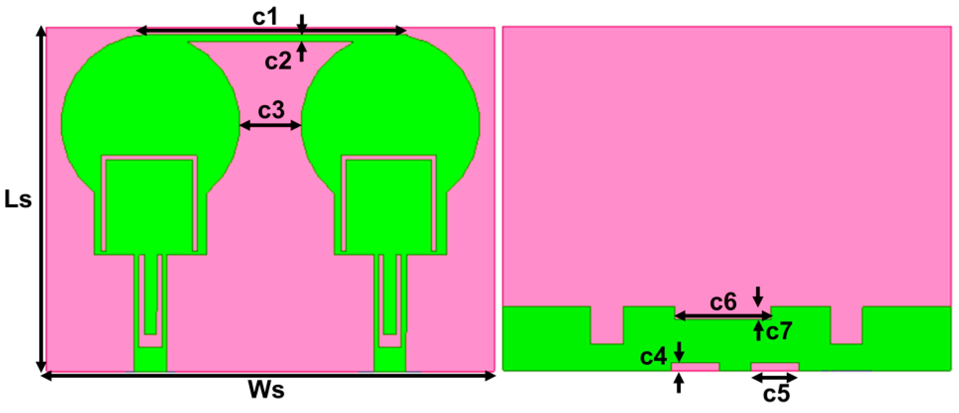
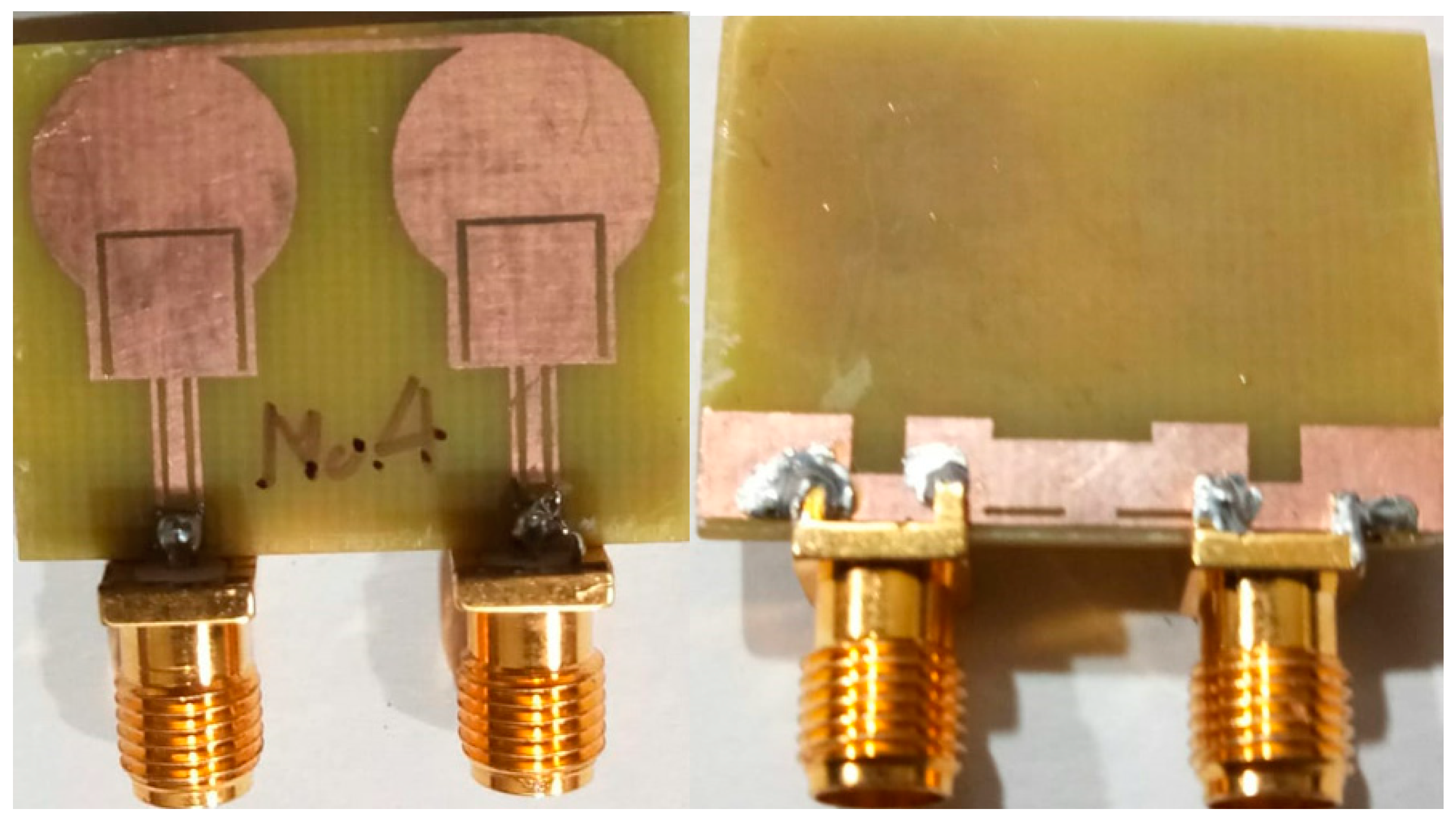
According to the literature, most MIMO antennas use DGS to improve isolation, and the interelement separation is rather large. This work describes a unique two-port UWB MIMO antenna with a decoupling mechanism as a neutralization line. Impedance matching for the UWB spectrum is performed using a hybrid structure composed of a circular monopole with a rectangle as a radiator and a decreased ground plane. The lowered ground plane creates a local current channel, which aids in achieving a broader impedance bandwidth. U-shape slots are carved on the radiator to accomplish dual band-notching at WLAN and X-band frequencies. The band-notched monopole UWB antenna is horizontally recreated with a much less than quarter wavelength separation (i.e., 3.8 mm or 0.04 λ, λ is computed using a lower frequency of 3.4 GHz). The coupling effect among the elements is reduced using a neutralization line. The projected antenna has physical dimensions of 21.5 × 28 × 1.6 mm3 (0.24 × 0.31 × 0.01 λ3) with an impedance bandwidth of 112% (3.4 to 12.2 GHz) and isolation greater than 16 dB throughout the operating frequencies. Furthermore, the projected antenna is investigated for characteristic mode analysis (CMA), MIMO diversity characteristics, and time-domain features. For experimental validation, the proposed design is printed on an FR4 substrate ().
Novelty and Contributions
The following are the significant contributions of this work:
The efficacious and simple UWB monopole design achieves a reflection coefficient curve of less than −17 dB throughout the entire working frequency range.
The controllable dual notch frequencies are achieved at the WLAN and complete X-band (uplink and downlink) satellite frequency bands.
To construct the two-port dual-notch UWB antenna, the intended dual-notched UWB antenna is reproduced with a minimum 3.8 mm separation parallelly.
The proposed MIMO antenna is evaluated for the characteristic mode analysis (CMA), MIMO diversity features, and time-domain characterization.
The remainder of the study is structured as follows: The detailed antenna design and its evolution are presented in
Section 2.
Section 3 outlines the decoupling mechanism designed to achieve the optimal isolation of the projected antenna.
Section 4 provides the findings of the CMA. The performance characteristics of the projected design are illustrated in
Section 5.
Section 6 provides concluding remarks.
3. Decoupling Mechanism
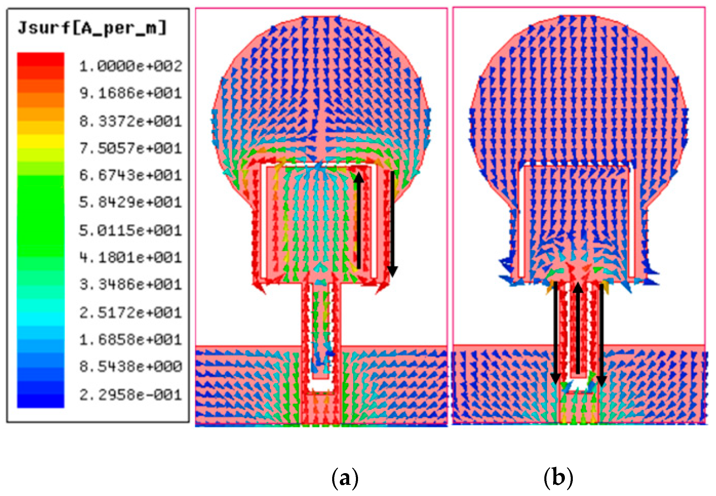
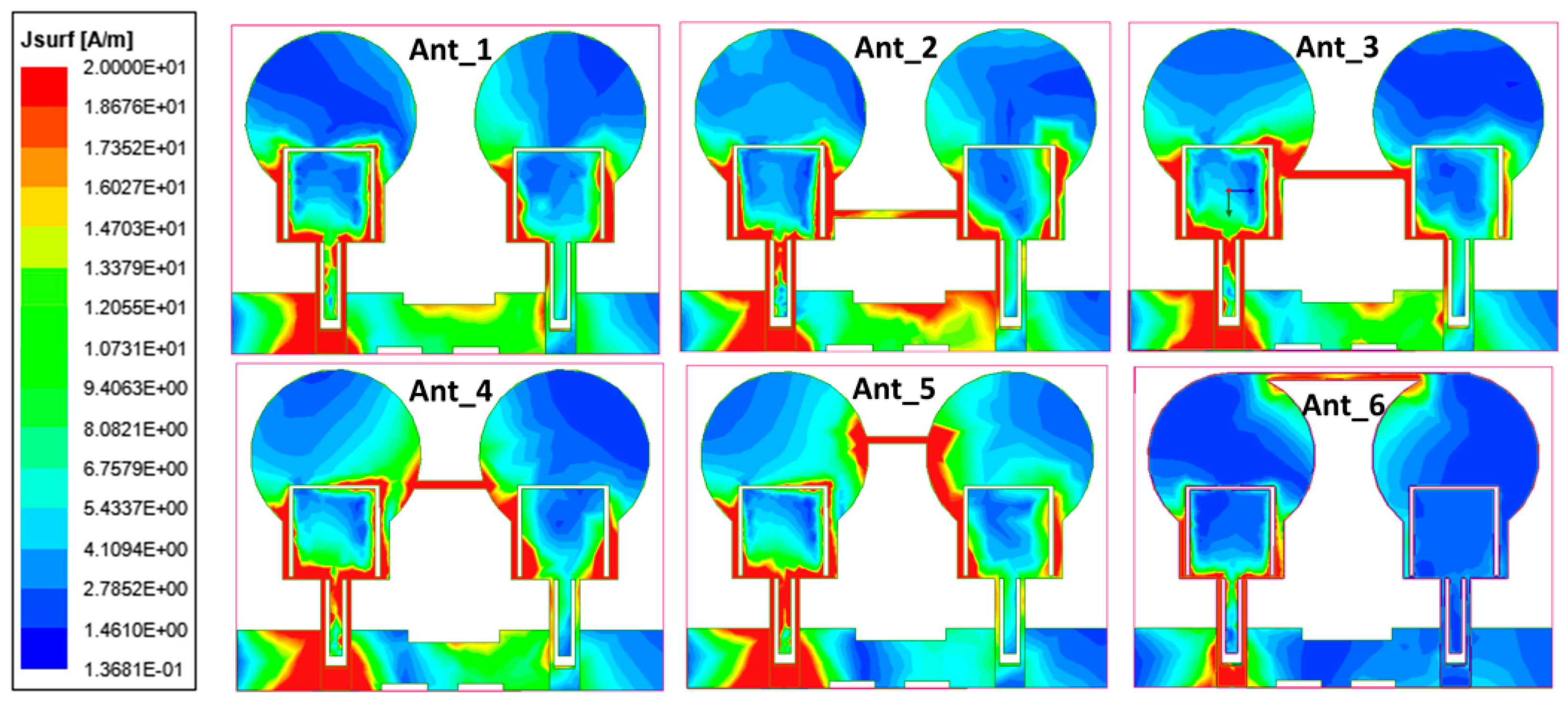
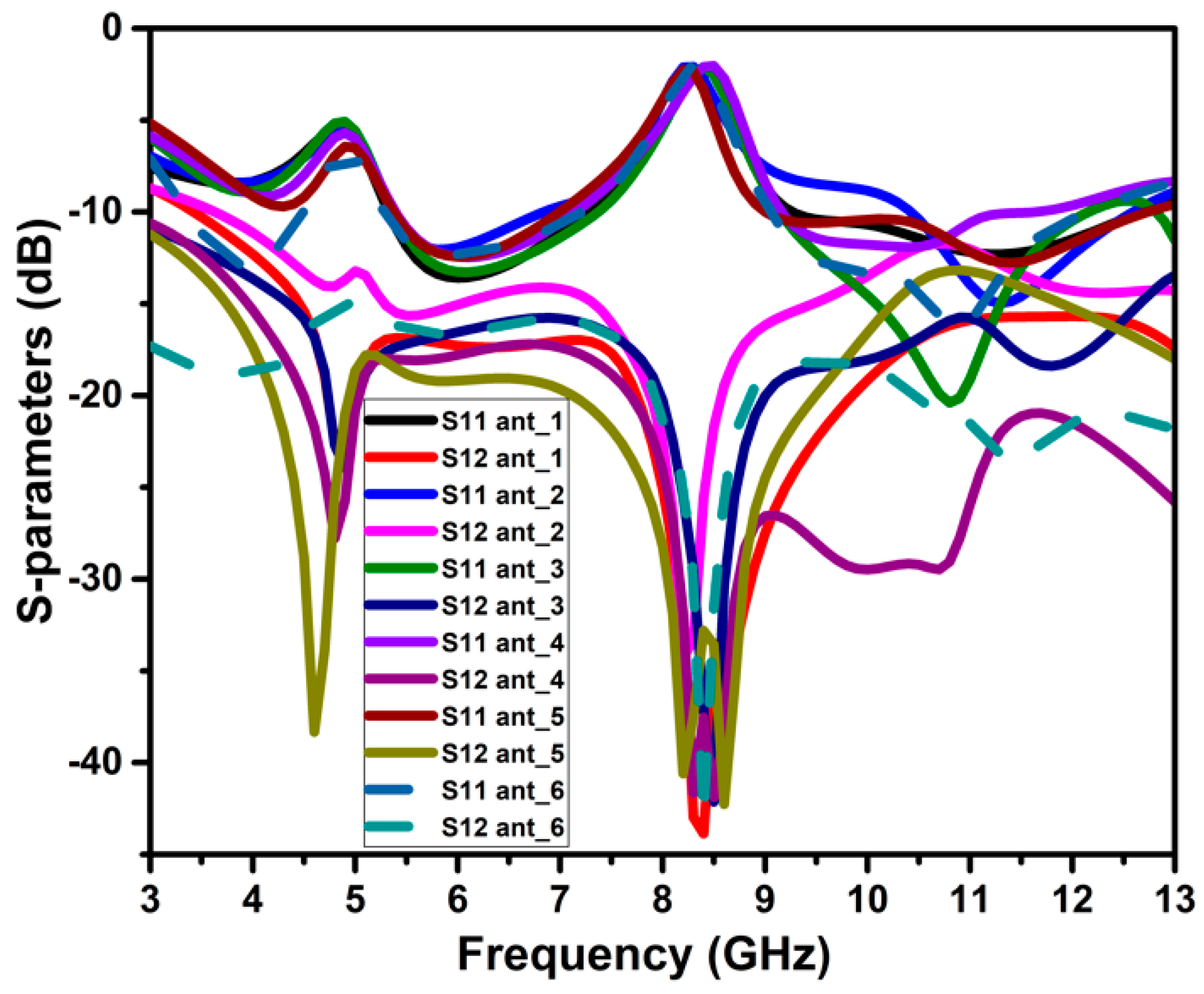
The isolation enhancement process is analyzed by plotting the surface current distribution of the projected antenna, as portrayed in
Figure 10. Current distribution graphs are obtained by stimulating one port and terminating the other port with matched conditions. The projected antenna without a neutralization line has a significant coupling effect on the neighboring element, as depicted in
Figure 10 ant_1. Positioning the neutralization line (NL) onto the radiator is the most challenging step in using the neutralization line as a decoupling element. NL is originally placed near the middle of the antenna where the largest current concentration is present, based on the current distribution in
Figure 10 ant_1. As in
Figure 10 ant_2-ant_6, the position of NL is shifted upwards by observing the current distribution plots and their S-parameter curve at a specific placement referred to as ant_1 to ant_6. The S-parameter curve for each arrangement is illustrated in
Figure 11. The ant_6 arrangement provides the out-of-phase current to that of the coupling current, resulting in improved isolation, as demonstrated in
Figure 12.
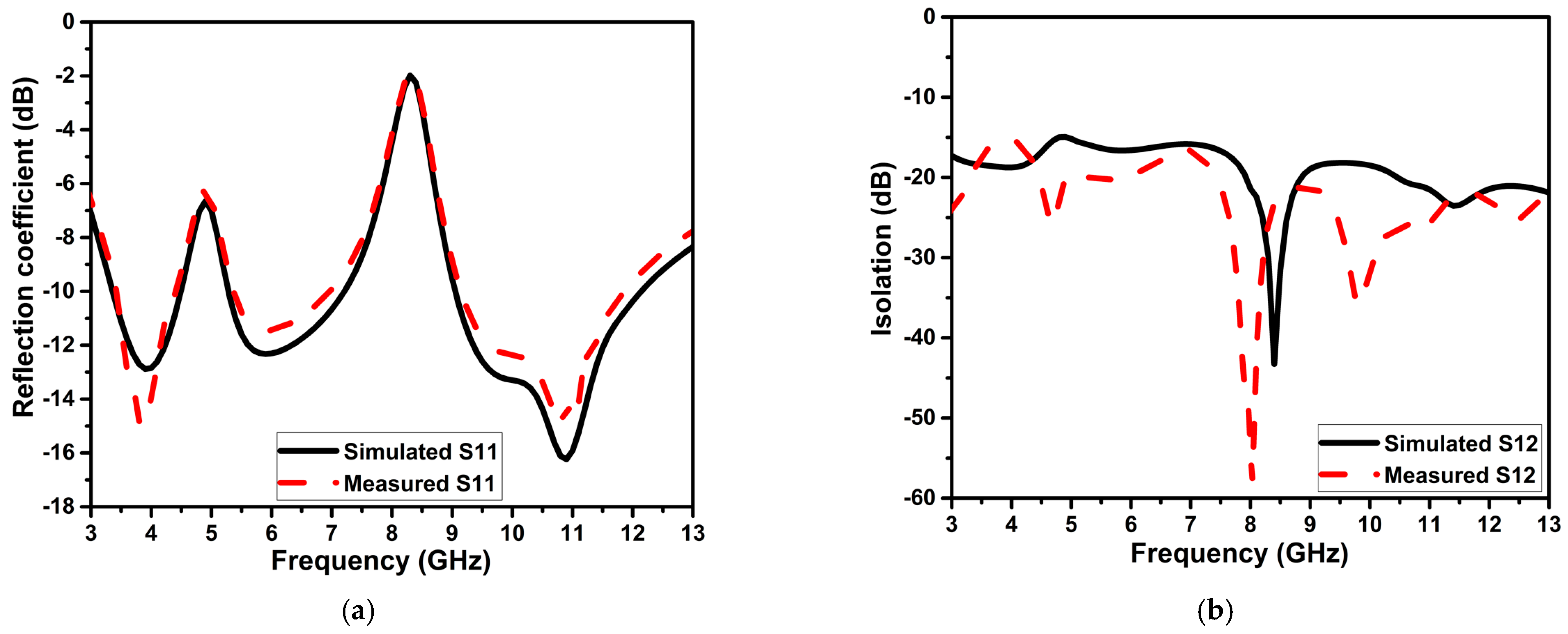
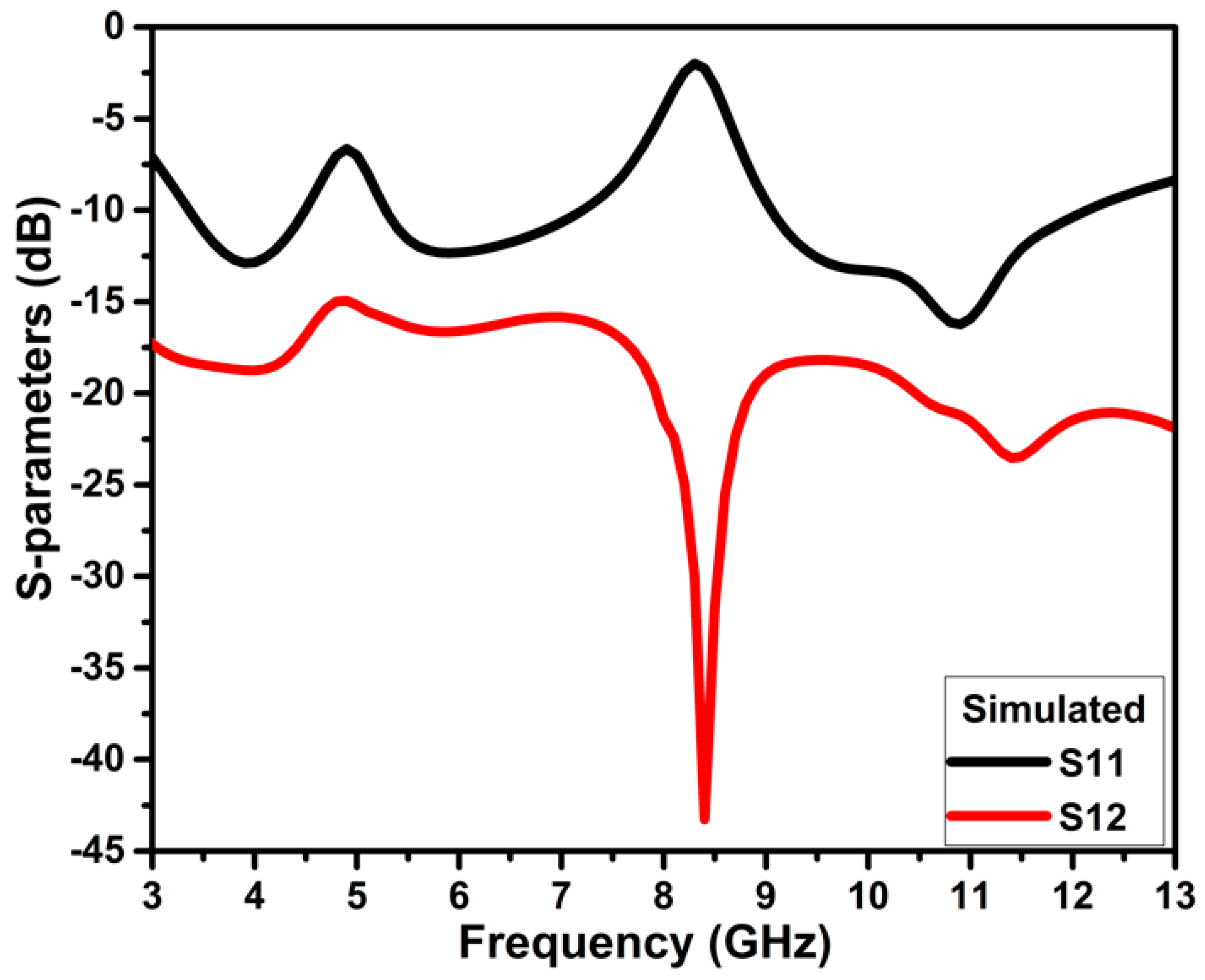
It is clear from
Figure 11 that ant_1 to ant_5 have poor isolation and reflection coefficient values, particularly at lower frequencies. The ant_6 arrangement provides isolation greater than 16 dB throughout the impedance bandwidth from 3.4–12.1 GHz.
4. CMA
Robert J. Garbacz’s 1965 study, “Introduction of modal expansion in electromagnetic scattering on resonance region”, was the first to examine the fundamental theory of CMA [
21,
22]. The total current that flows through a conducting or radiating structure generated by an incoming electromagnetic field may be described as the weighted sum of N transverse eigencurrents (
) that are geometrical and material reliant while being self-reliant on the excitation vector, according to a key concept of CMA theory [
23,
24]. The total current can be expressed as in Equation (6)
where
is modal weight coefficients that calculate the impact of each eigencurrent on the overall current. Because each eigencurrent generates its electric field, the overall current generates the total radiated electric field. The modal significance (
MS) is a significant metric of the CMA that determines each mode’s maximum normalized current strength and influences the radiation properties of that particular mode [
25]. The MS can be calculated using Equation (7)
where
is the eigenvalue of the
ith mode and is related to the eigencurrents using a method of moment matrix (
), as follows:
where
R and
X depict the real and imaginary part of the impedance
Z. The eigenvalues help analyze the capacitance and inductance values; their significance is listed in
Table 4. The phase difference in the electric field and surface current of the antenna is described by the characteristic angle (CA). The CA (
) can be computed using Equation (10)
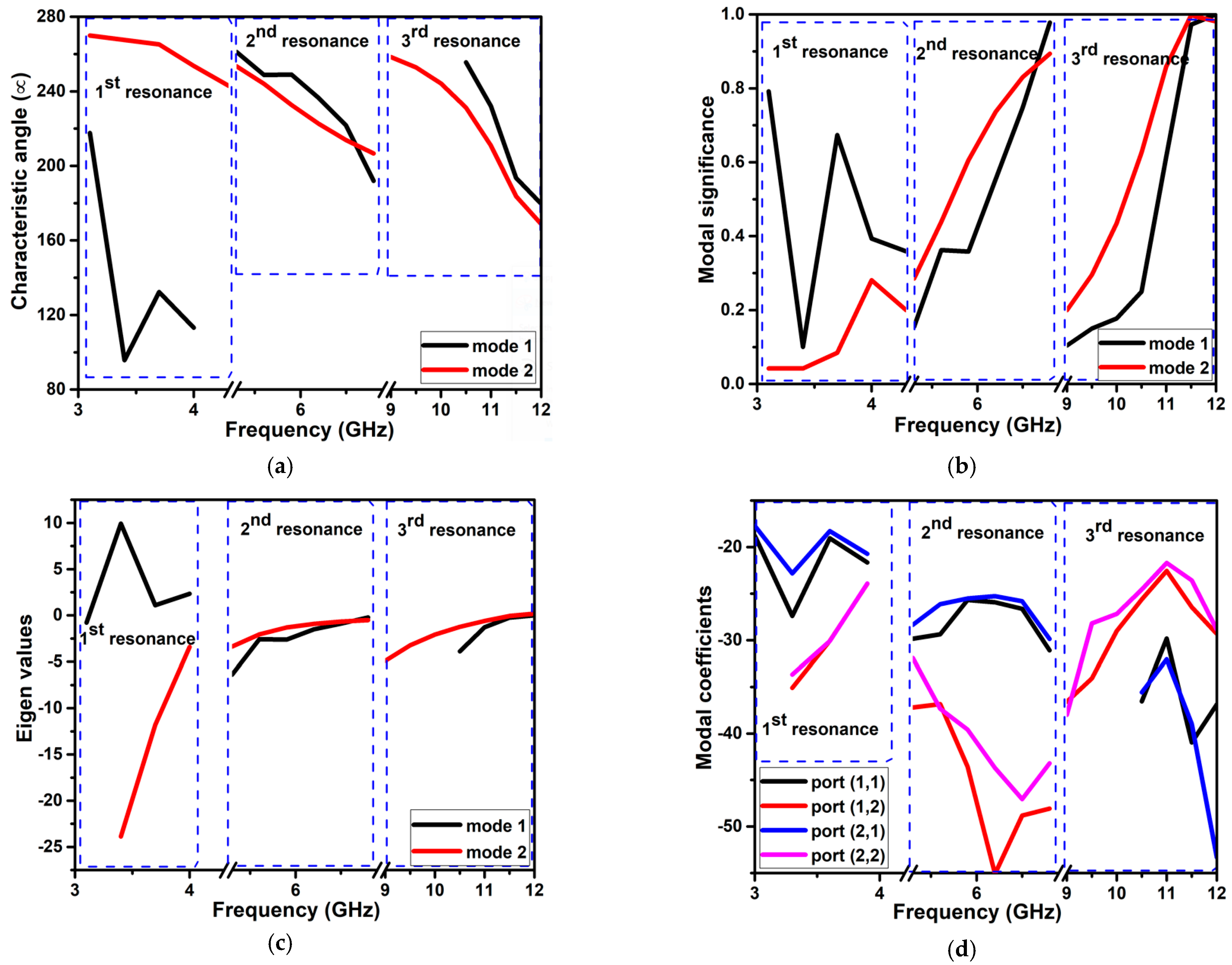
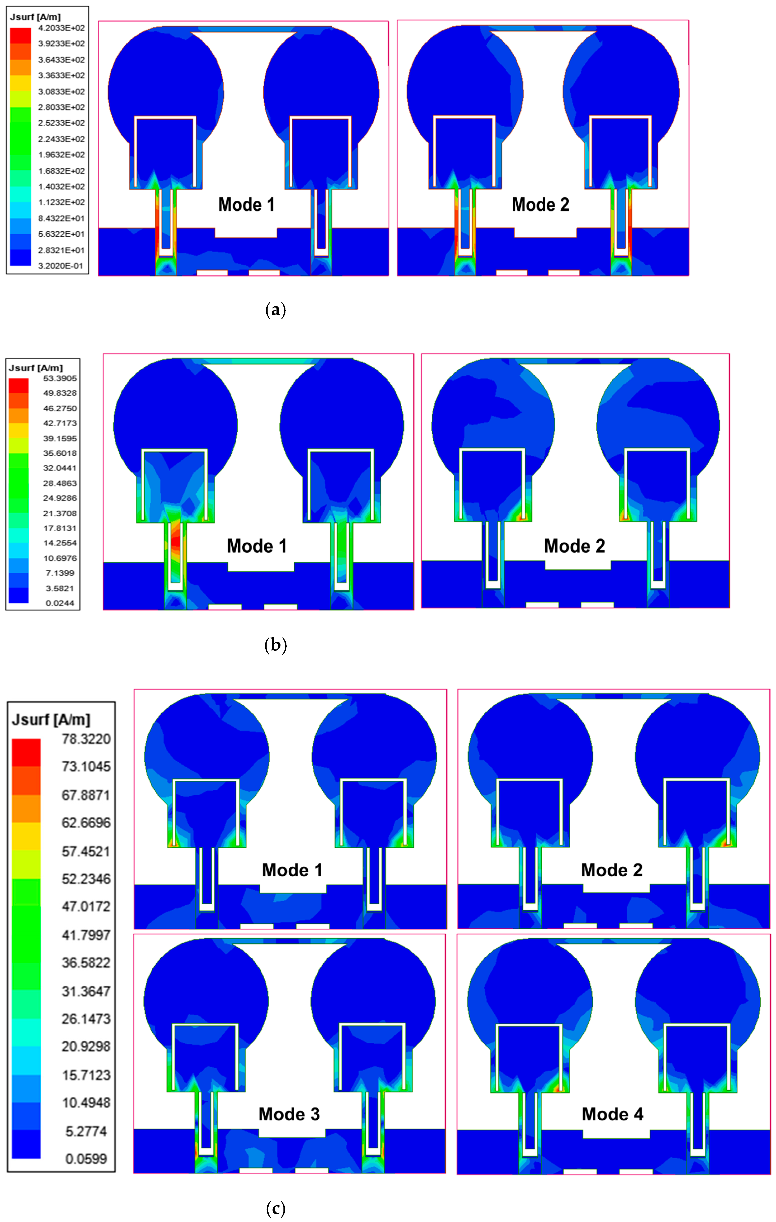
CMA was carried out on the projected two-port antenna. At the principal frequency resonance of 3.7 GHz, mode 1 has an MS of 0.7, eigenvalue of 1.09, and CA of 132 degrees. Other modes have lower significance values at this frequency, i.e., MS < 0.1. The nature of this induced mode is inductive. Similarly, at the second resonance frequency of 6.8 GHz, there are two significant modes, 1 and 2. Both the modes are capacitive in nature. Modes 1, 2, 3, and 4 are induced at the subsequent resonance frequency of 11.5 GHz. The first three modes are capacitive, and mode 4 is inductive. The CA, MS, eigenvalue, and modal coefficient curves of the projected design at the working band are illustrated in
Figure 13, and their values at the frequencies of 3.7 GHz, 6.8 GHz, and 11.5 GHz are listed in
Table 5.
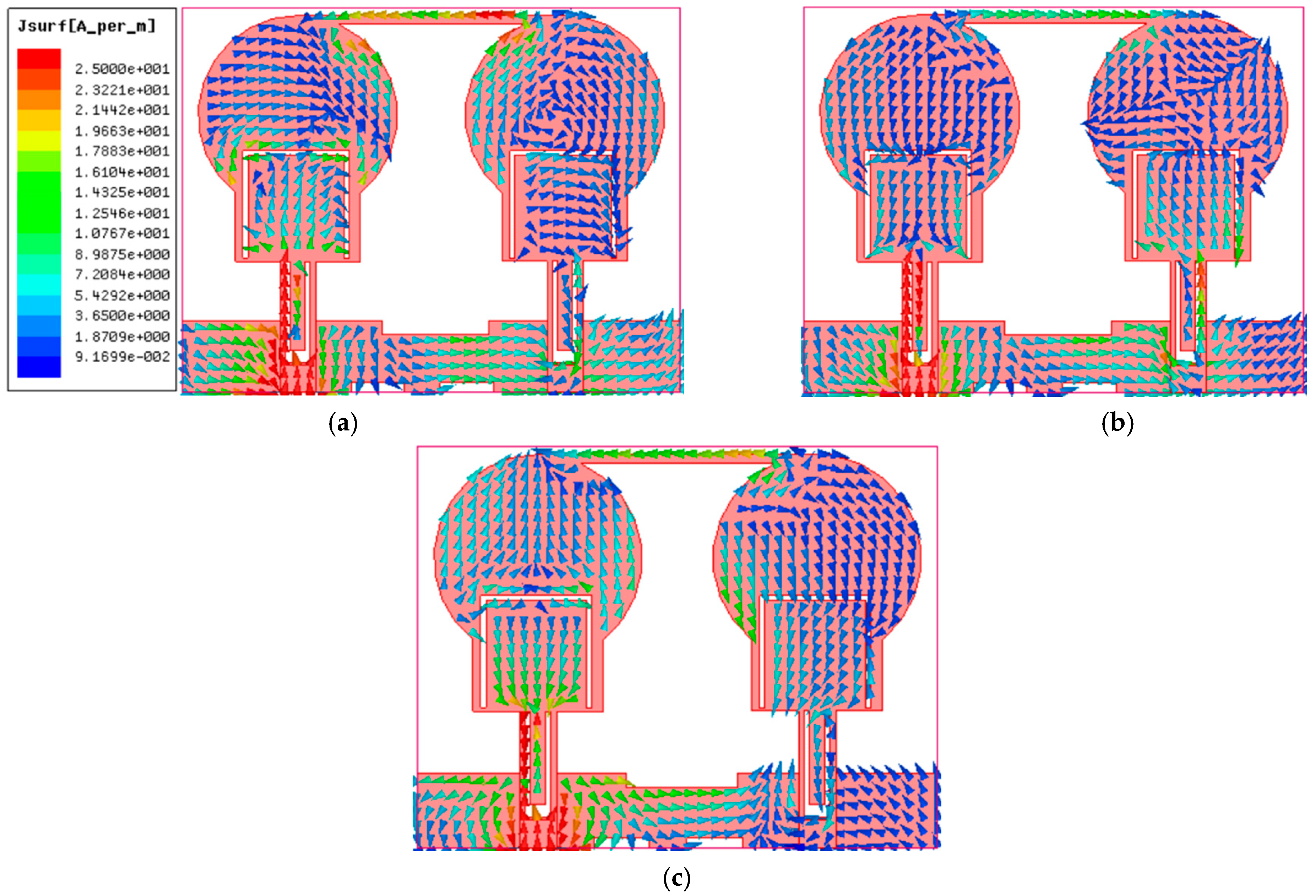
Figure 13d shows the modal coefficients between the ports. These coefficients influence the eigencurrent, which generates the overall current and the radiated electric field. The surface current distribution over these frequencies in different modes is illustrated in
Figure 14.
6. Conclusions
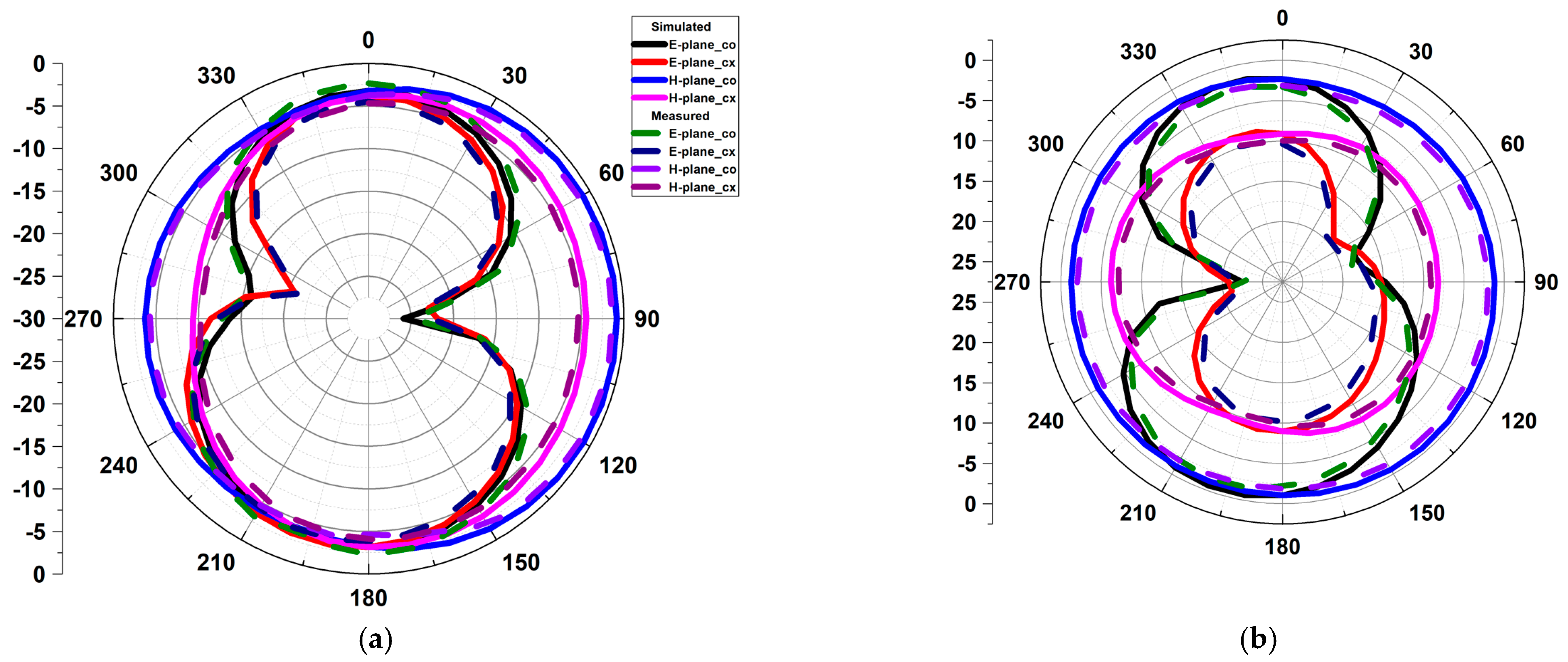
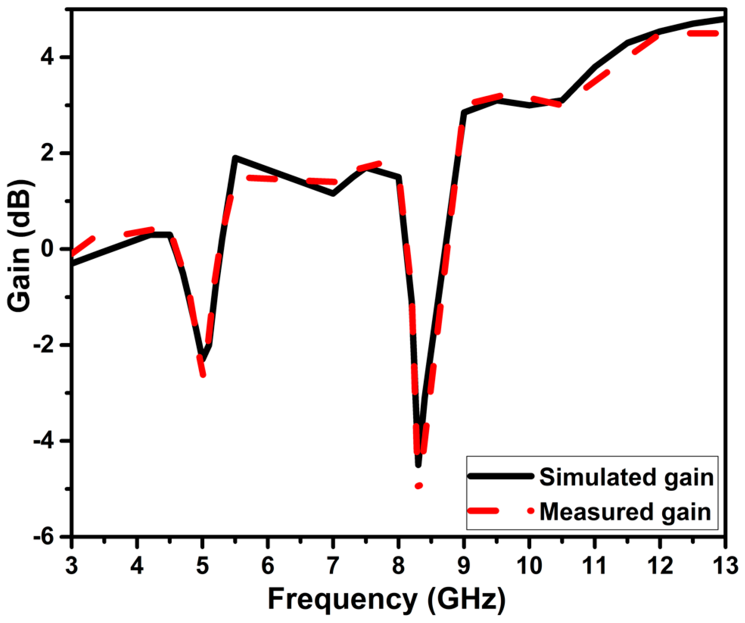
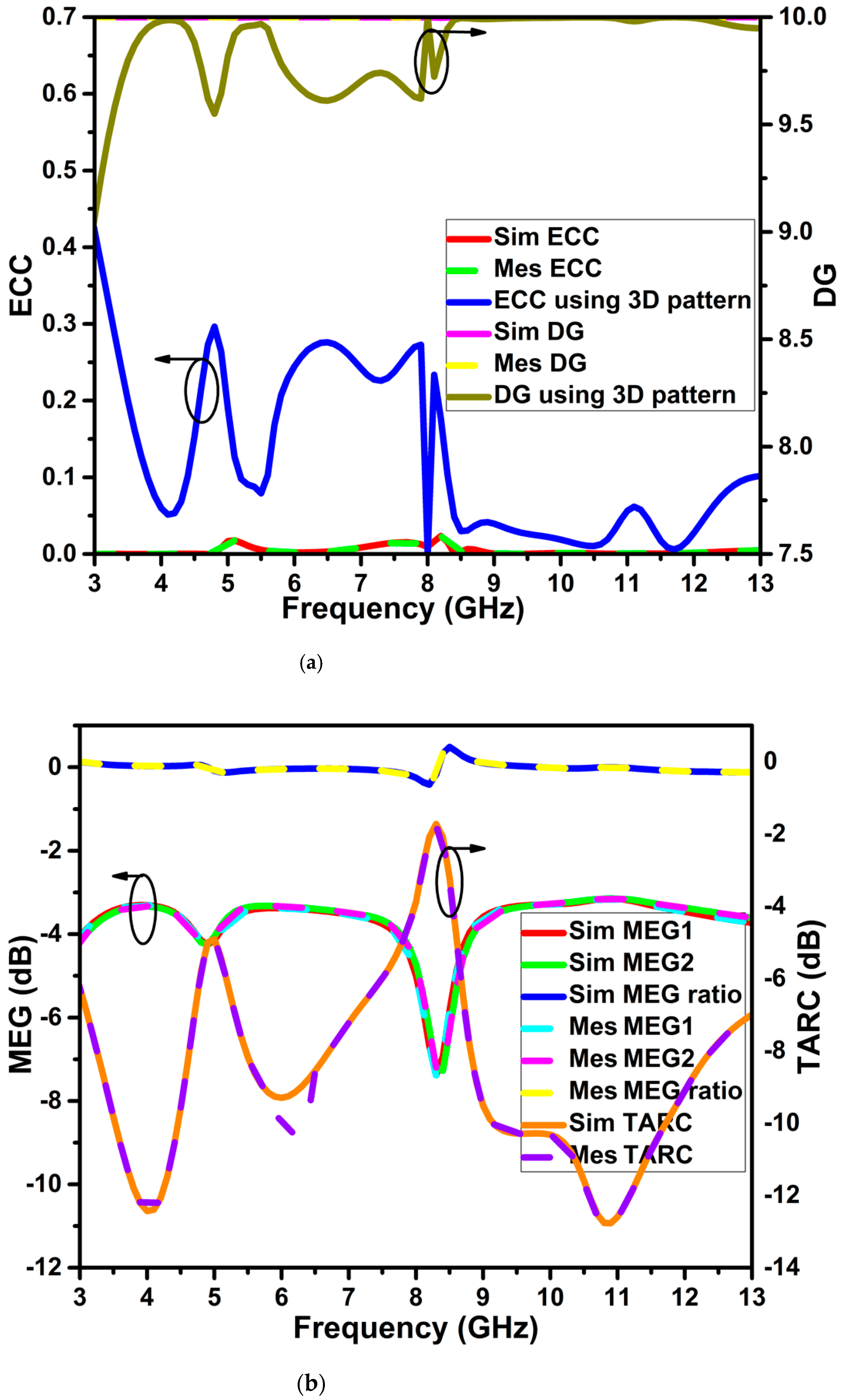
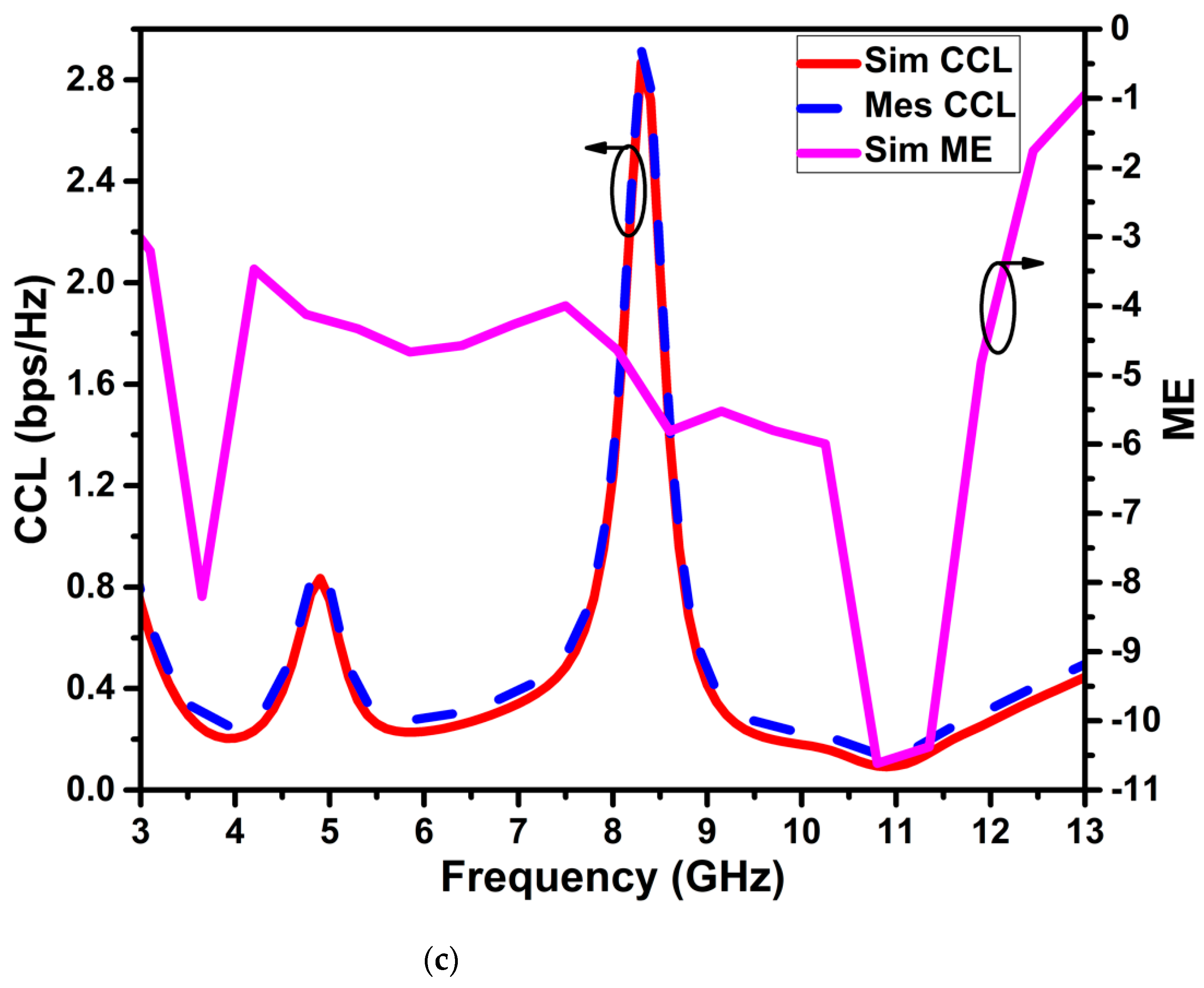
This study presents a two-port, dual band-notch UWB antenna based on neutralization line (NL). The NL serves as a decoupling device in the connection between the two similarly situated dual band-notch UWB antennas. The NL improves the MIMO system’s isolation between the antenna elements by producing the opposing current to the coupling current. The proposed design has a simple and effective structure with compact dimensions of 0.24 × 0.31 × 0.01 λ3, operating in the frequency range of 3.4 to 12.1 GHz, except for the frequency band notching of 4.5–5.3 GHz and 7.2–9 GHz. The port-to-port isolation is greater than 16 dB across the impedance bandwidth. The time-domain characteristics GD is less than 1 ns except for the notched frequency bands, and FF is greater than 0.96 in side-to-side and face-to-face orientation. The MIMO diversity parameters have ECC< 0.3, DG > 9.6 dB, MEG < −3 dB, TARC < −10 dB, CCL < 0.3 bps/Hz, and ME < −2 dB across the operational frequency, all other than the serrated bands, and characteristic mode analysis are also considered for the antenna design. The projected antenna is suitable for MIMO wireless communication, according to the numerical and experimental results. Future studies will concentrate on expanding the number of sending and receiving antennas to increase the channel capacity. The proposed decoupling approach can also be integrated with other ways as a hybrid decoupling structure to improve isolation among the antenna elements.


