
Compact Full Ka-Band Waveguide Directional Coupler Based on Rectangular Aperture Array with Stairs


Abstract
:
1. Introduction
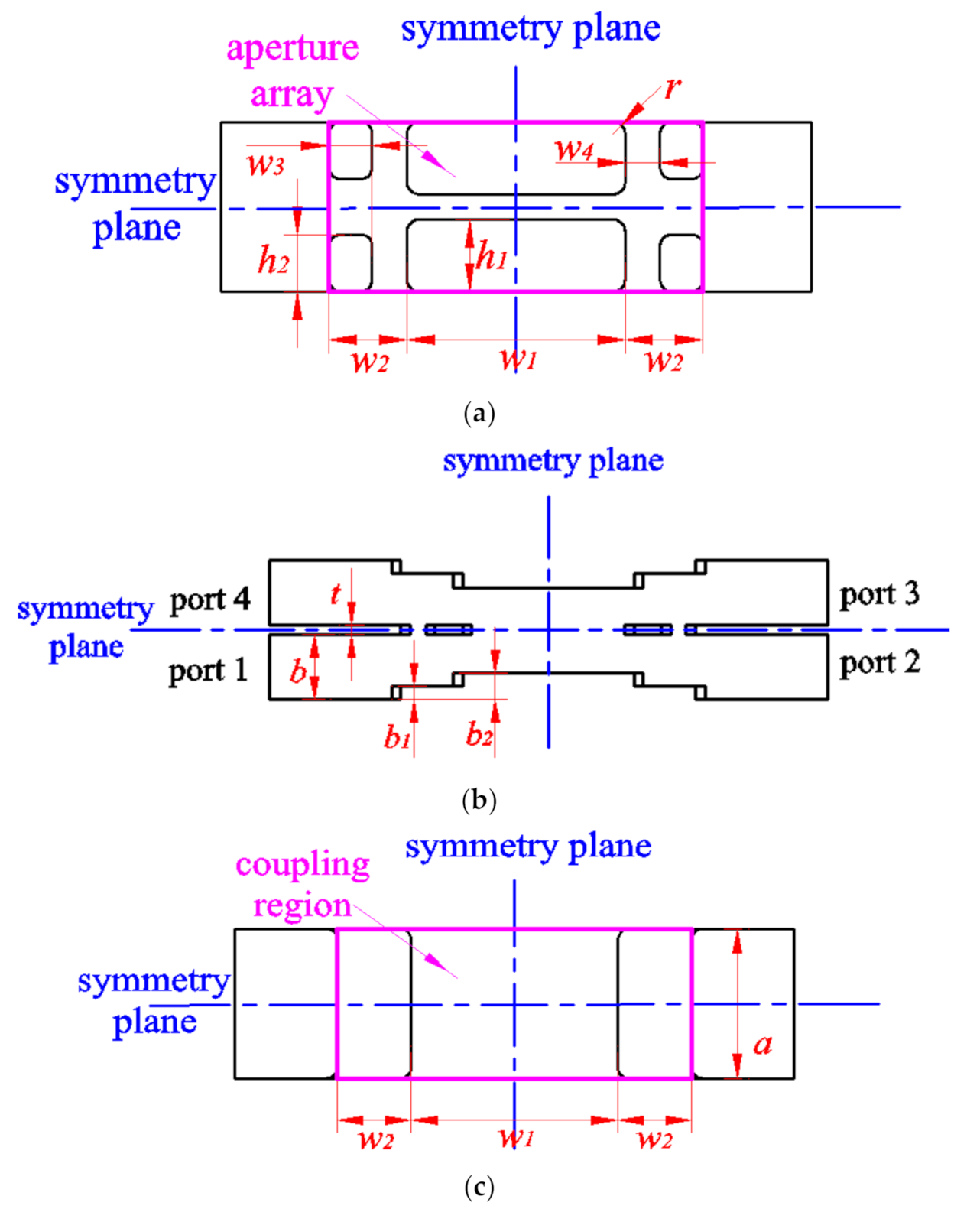
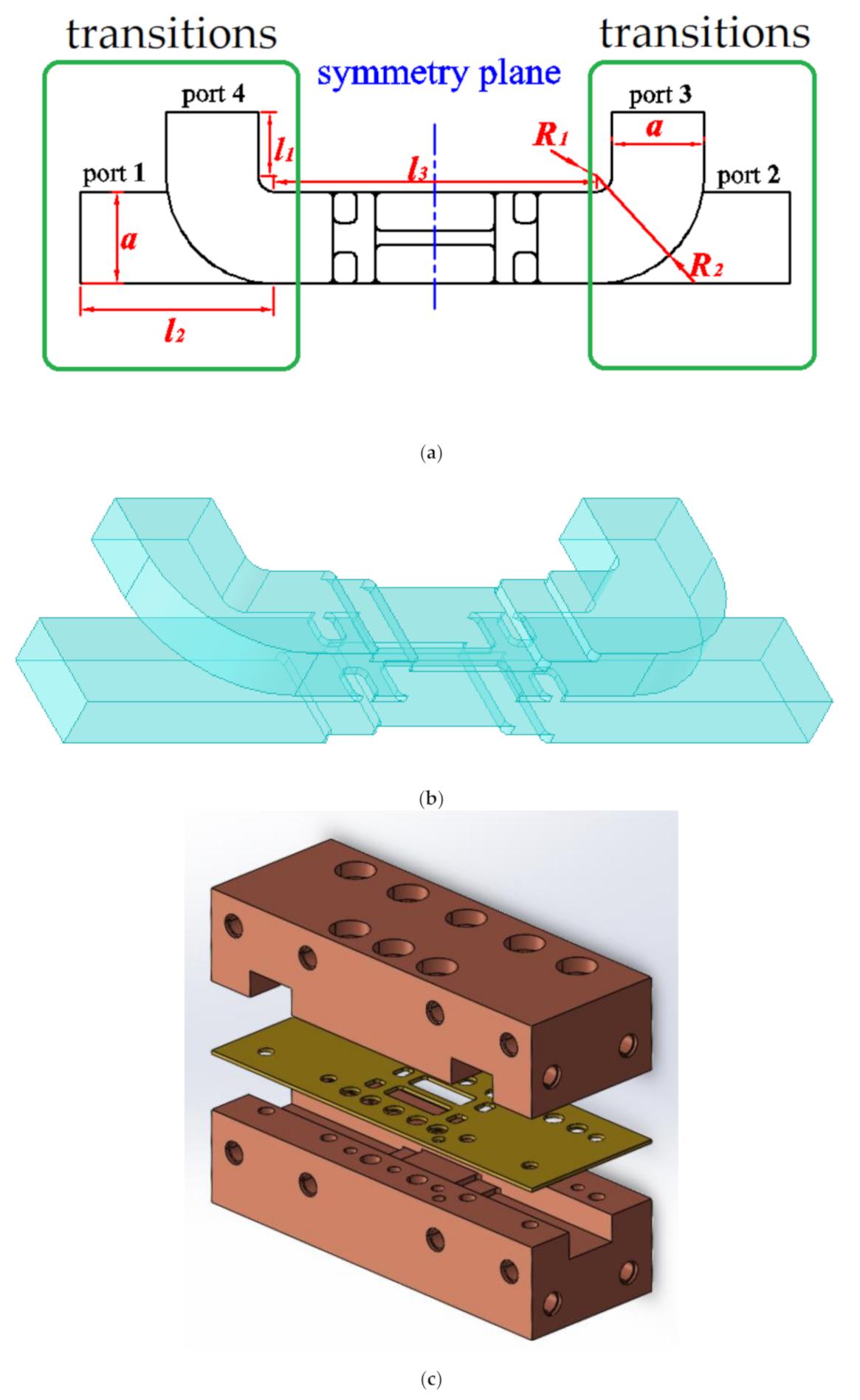
2. Coupler Configuration
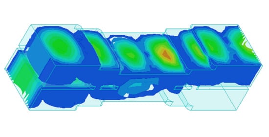
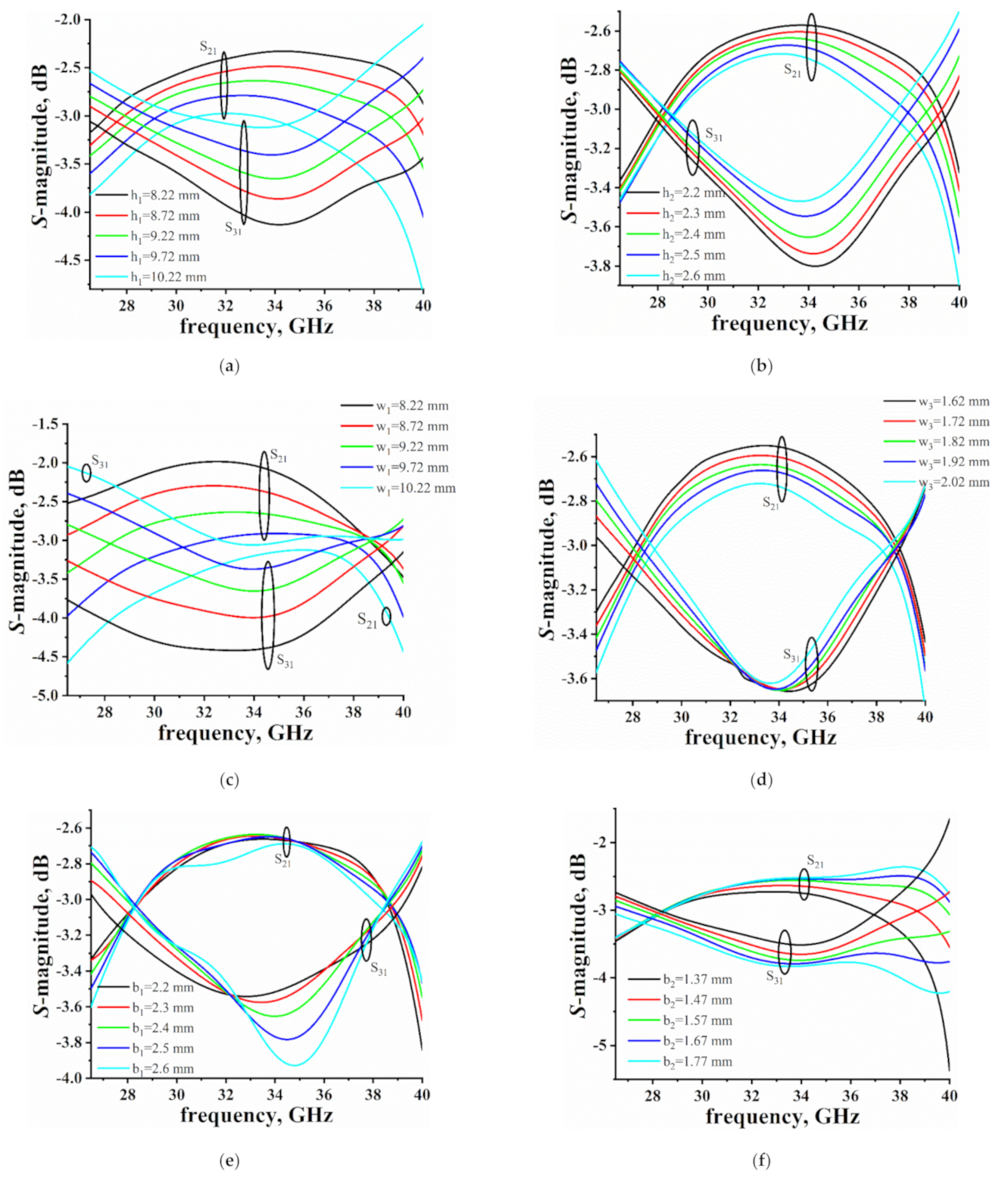
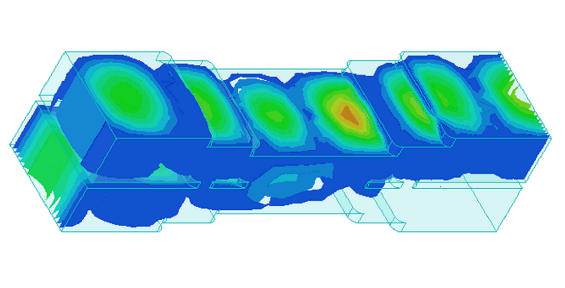
3. Coupler Design and Simulation Results
4. Results
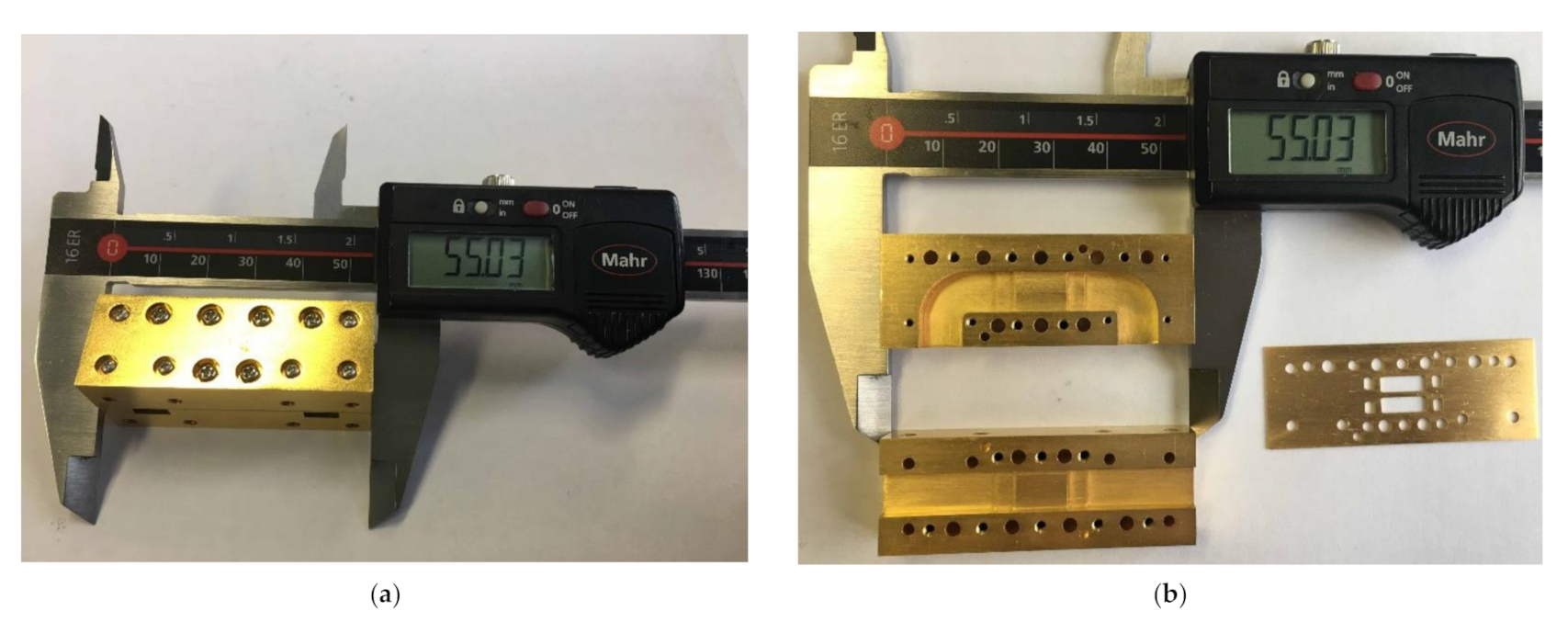
4.1. Fabrication
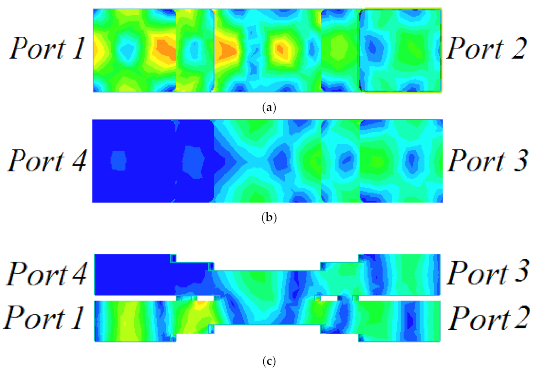
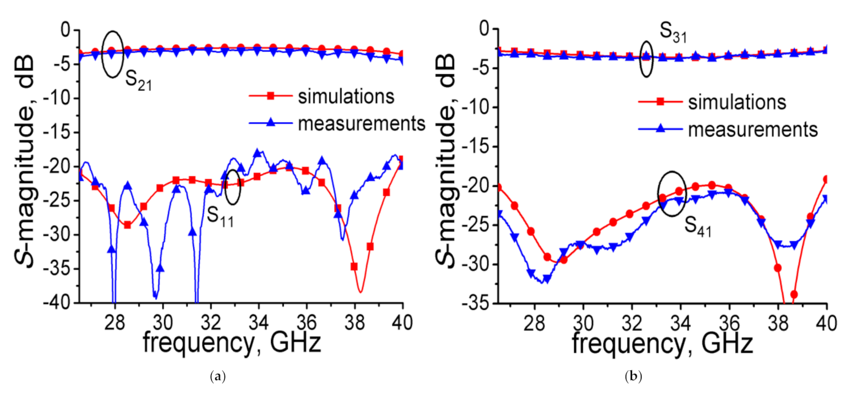
4.2. Measurement Results
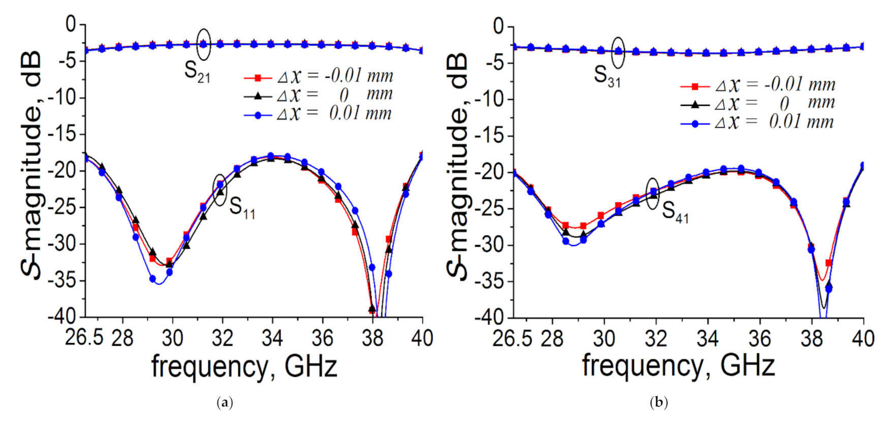
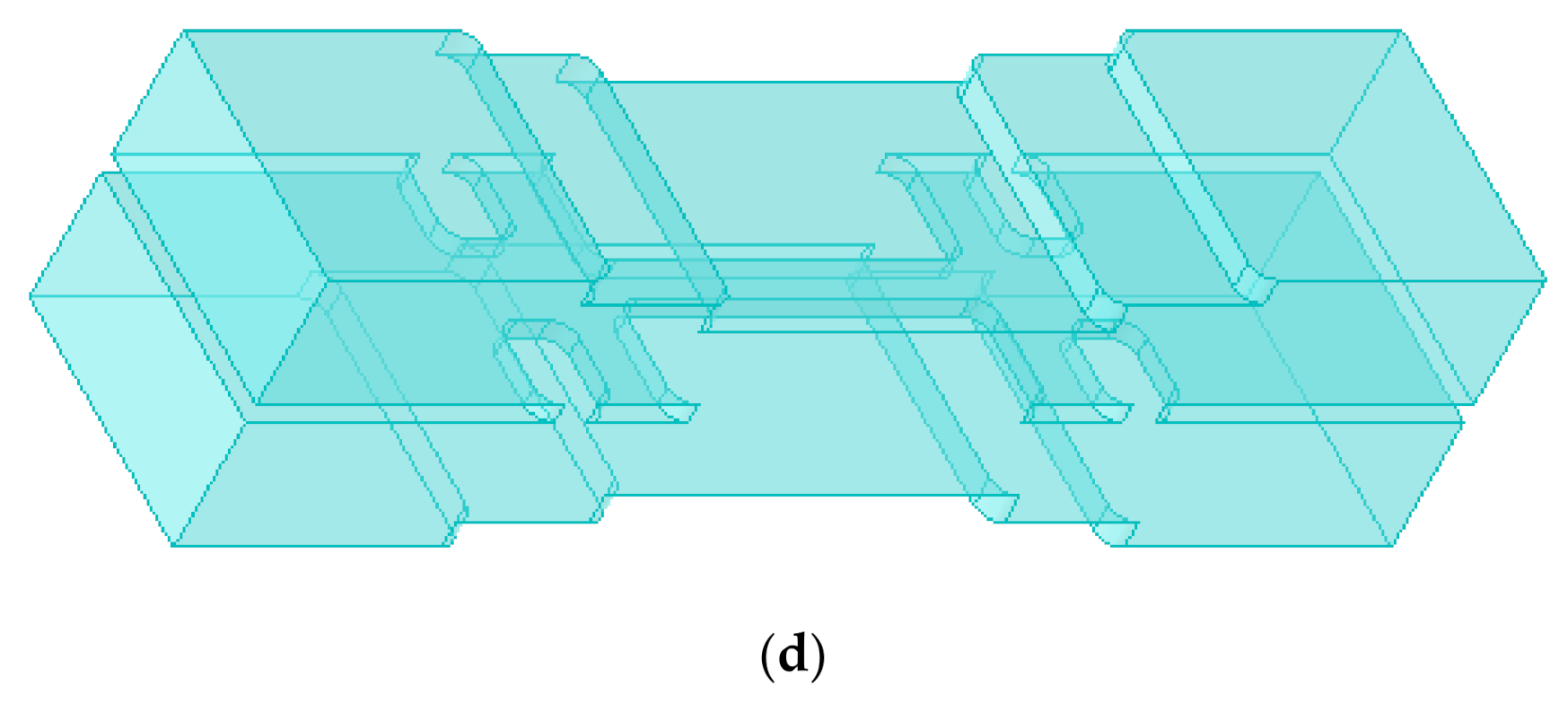
4.3. Sensitivity Analysis
5. Conclusions
6. Patents
Author Contributions
Funding
Institutional Review Board Statement
Informed Consent Statement
Data Availability Statement
Conflicts of Interest
References
- Bethe, H.A. Theory of diffraction by small holes. Phys. Rev. 1944, 66, 163. [Google Scholar] [CrossRef]
- Kawai, T.; Kishihara, M.; Kokubo, Y.; Ohta, T. Cavity-type directional couplers with simple structure. In Proceedings of the 1997 IEEE MTT-S International Microwave Symposium Digest, Denver, CO, USA, 8–13 June 1997; pp. 413–416. [Google Scholar]
- Riblet, H.J. The short-slot hybrid junction. Proc. IRE 1952, 40, 180–184. [Google Scholar] [CrossRef]
- Hildebrand, L.T. Results for a simple compact narrow-wall directional coupler. IEEE Microw. Guided Wave Lett. 2000, 10, 231–232. [Google Scholar] [CrossRef]
- Levy, R. Analysis and synthesis of waveguide multiaperture directional couplers. IEEE Trans. Microw. Theory Tech. 1968, 16, 995–1006. [Google Scholar] [CrossRef]
- Yeo, S.; Lee, K. Improvements in design of six-port reflectometer comprising symmetrical five-port waveguide junction and directional coupler. IEEE Trans. Instrum. Meas. 1990, 39, 184–188. [Google Scholar] [CrossRef]
- Niu, Z.; Zhang, B.; Ji, D.; Yang, Y.; Liu, Y.; Feng, Y.; Fan, Y.; Chen, Z.; Chen, X.; Li, D. A Novel 3-dB Waveguide Hybrid Coupler for Terahertz Operation. IEEE Microw. Wirel. Compon. Lett. 2019, 29, 273–275. [Google Scholar] [CrossRef]
- Liu, S.; Xu, F. Compact multilayer half mode substrate integrated waveguide 3-dB coupler. IEEE Microw. Wirel. Compon. Lett. 2018, 28, 564–566. [Google Scholar] [CrossRef]
- Wang, K.; Shea, D.; Zhang, X.; Yuan, H. Wideband 3-dB Coupler Based on Substrate Integrated Gap Waveguide. In Proceedings of the 2018 International Conference on Microwave and Millimeter Wave Technology (ICMMT), Chengdu, China, 7–11 May 2018; pp. 1–3. [Google Scholar]
- Longhi, M.; Galdeano, J.; Morini, A.; Baldelli, M.; Angeletti, P.; Toso, G.; Venanzoni, G. Dual-polarization beam forming networks based on high order directional couplers. In Proceedings of the 2017 11th European Conference on Antennas and Propagation (EUCAP), Paris, France, 19–24 March 2017; pp. 2820–2823. [Google Scholar]
- Doghri, A.; Djerafi, T.; Ghiotto, A.; Wu, K. Substrate integrated waveguide directional couplers for compact three-dimensional integrated circuits. IEEE Trans. Microw. Theory Tech. 2014, 63, 209–221. [Google Scholar] [CrossRef] [Green Version]
- Ali, M.M.M.; Shams, S.I.; Sebak, A. Ultra-wideband printed ridge gap waveguide hybrid directional coupler for millimetre wave applications. IET Microw. Antennas Propag. 2019, 13, 1181–1187. [Google Scholar]
- Miralles, E.; Belenguer, A.; Esteban, H.; Boria, V. Cross guide Moreno directional coupler in empty substrate integrated waveguide. Radio Sci. 2017, 52, 597–603. [Google Scholar] [CrossRef]
- Tavakoli, M.J.; Mallahzadeh, A.R. Wideband directional coupler for millimeter wave application based on substrate integrated waveguide. Emerg. Sci. J. 2018, 2, 93–99. [Google Scholar] [CrossRef] [Green Version]
- Veadesh, B.; Aswin, S.; Shambavi, K. Design and analysis of C-band SIW directional coupler. In Proceedings of the 2017 International conference on Microelectronic Devices, Circuits and Systems (ICMDCS), Vellore, India, 10–12 August 2017; pp. 1–5. [Google Scholar]
- Parment, F.; Ghiotto, A.; Vuong, T.-P.; Duchamp, J.-M.; Wu, K. Air-to-dielectric-filled two-hole substrate-integrated waveguide directional coupler. IEEE Microw. Wirel. Compon. Lett. 2017, 27, 621–623. [Google Scholar] [CrossRef]
- Chandrasekaran, K.; Alphones, A.; Karim, M. Graded index substrate integrated waveguide based directional coupler. In Proceedings of the 2017 IEEE International Symposium on Antennas and Propagation & USNC/URSI National Radio Science Meeting, San Diego, CA, USA, 9–14 July 2017; pp. 2255–2256. [Google Scholar]
- Zhang, Y.; Wang, Q.; Xin, H. A Compact 3 dB E-Plane Waveguide Directional Coupler With Full Bandwidth. IEEE Microw. Wirel. Compon. Lett. 2014, 24, 227–229. [Google Scholar] [CrossRef]
- Cheng, Y.J.; Hong, W.; Wu, K.; Fan, Y. A hybrid guided-wave structure of half mode substrate integrated waveguide and conductor-backed slotline and its application in directional couplers. IEEE Microw. Wirel. Compon. Lett. 2011, 21, 65–67. [Google Scholar] [CrossRef]
- Fernandez, M.D.; Ballesteros, J.A.; Belenguer, A. Design of a hybrid directional coupler in empty substrate integrated waveguide (ESIW). IEEE Microw. Wirel. Compon. Lett. 2015, 25, 796–798. [Google Scholar] [CrossRef]
- Li, T.; Dou, W. Substrate integrated waveguide 3 dB directional coupler based on air-filled vias. Electron. Lett. 2017, 53, 611–613. [Google Scholar] [CrossRef]


| Coupler | Frequency(GHz) | Coupling Strength Imbalance (dB) | Bandwidth (%) | Relative Length | Type |
|---|---|---|---|---|---|
| [11] | 31–36.7 | ±0.54 | 16.8 | 1.41 × λg | SIW |
| [18] | 6.57–9.99 | ±0.6 | 41.3 | 3.37 × λg | RW |
| [19] | 10.675–13.325 | ±0.5 | 22.08 | 1.66 × λg | HMSIW |
| [20] | 13–17 | ±0.5 | 26.67 | 1.41 × λg | ESIW |
| [21] | 33–37 | ±0.33 | 11.43 | 0.71 × λg | SIW |
| This work | 26.5–40 | ±0.53 | 40.6 | 1.35 × λg | RW |
| Number of Apertures | Coupling Imbalance (dB) | Through Flatness (dB) | Return Loss (dB) | Coupler Model |
|---|---|---|---|---|
| 3.17 ± 0.92 | 3.4 ± 1.2 | 15.19 |  | |
| 3.11 ± 0.7 | 3.23 ± 0.89 | 17.65 |  | |
| 3.14 ± 0.46 | 3.13 ± 0.48 | 18.68 |  |
Publisher’s Note: MDPI stays neutral with regard to jurisdictional claims in published maps and institutional affiliations. |
© 2021 by the authors. Licensee MDPI, Basel, Switzerland. This article is an open access article distributed under the terms and conditions of the Creative Commons Attribution (CC BY) license (https://creativecommons.org/licenses/by/4.0/).
Share and Cite
Deng, X.; Dong, G.; Dai, X.; Deng, J. Compact Full Ka-Band Waveguide Directional Coupler Based on Rectangular Aperture Array with Stairs. Micromachines 2021, 12, 745. https://doi.org/10.3390/mi12070745
Deng X, Dong G, Dai X, Deng J. Compact Full Ka-Band Waveguide Directional Coupler Based on Rectangular Aperture Array with Stairs. Micromachines. 2021; 12(7):745. https://doi.org/10.3390/mi12070745
Chicago/Turabian StyleDeng, Xida, Ge Dong, Xuan Dai, and Jinxiang Deng. 2021. "Compact Full Ka-Band Waveguide Directional Coupler Based on Rectangular Aperture Array with Stairs" Micromachines 12, no. 7: 745. https://doi.org/10.3390/mi12070745
APA StyleDeng, X., Dong, G., Dai, X., & Deng, J. (2021). Compact Full Ka-Band Waveguide Directional Coupler Based on Rectangular Aperture Array with Stairs. Micromachines, 12(7), 745. https://doi.org/10.3390/mi12070745