
Self-Controlled Cleaving Method for Silicon DRIE Process Cross-Section Characterization

 ,
,
Abstract
1. Introduction
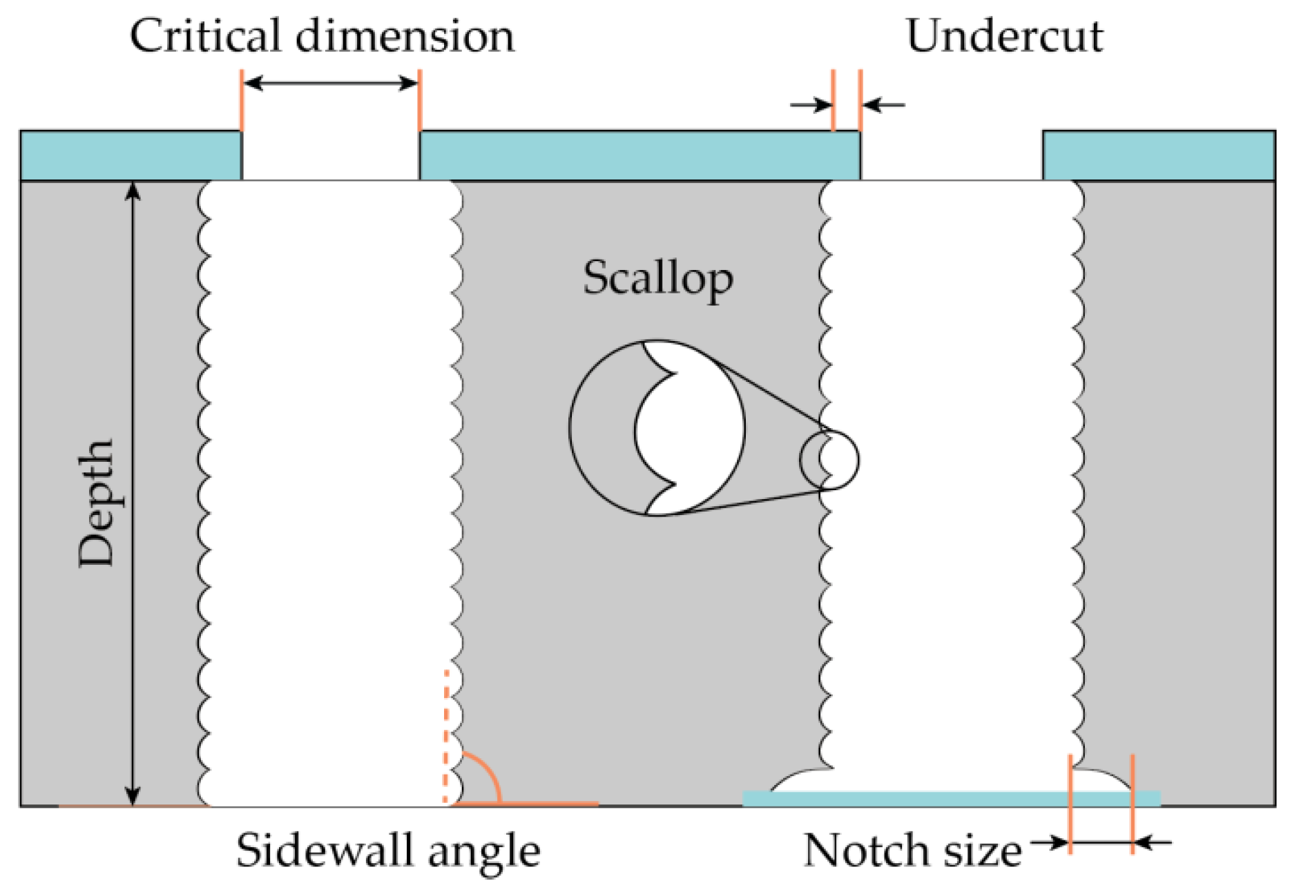
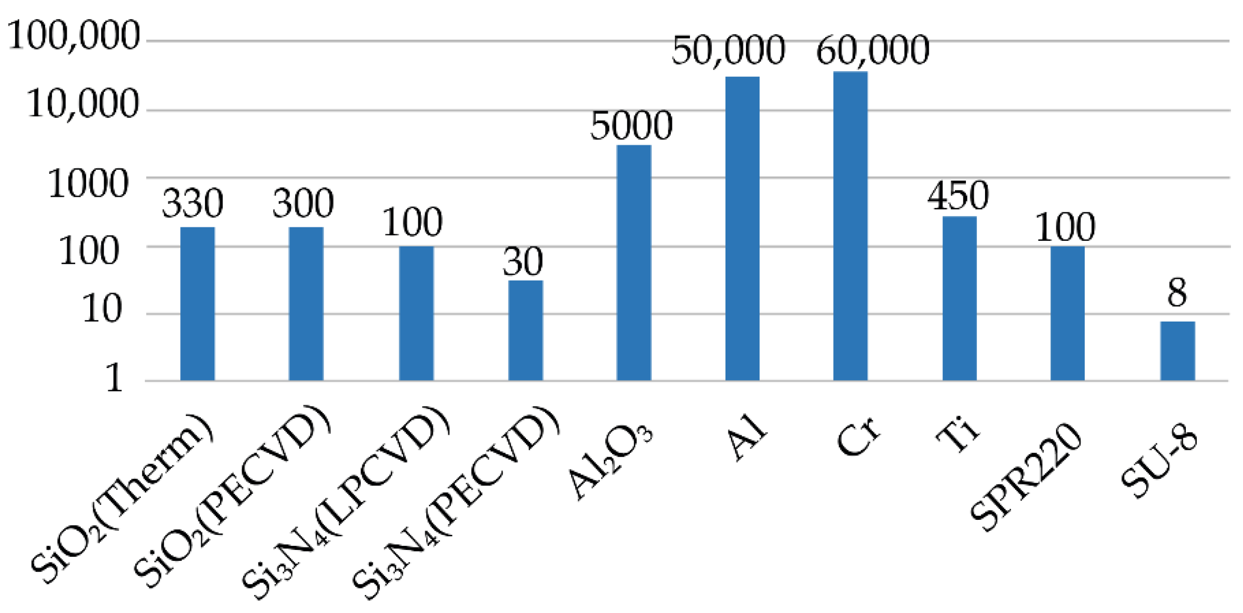
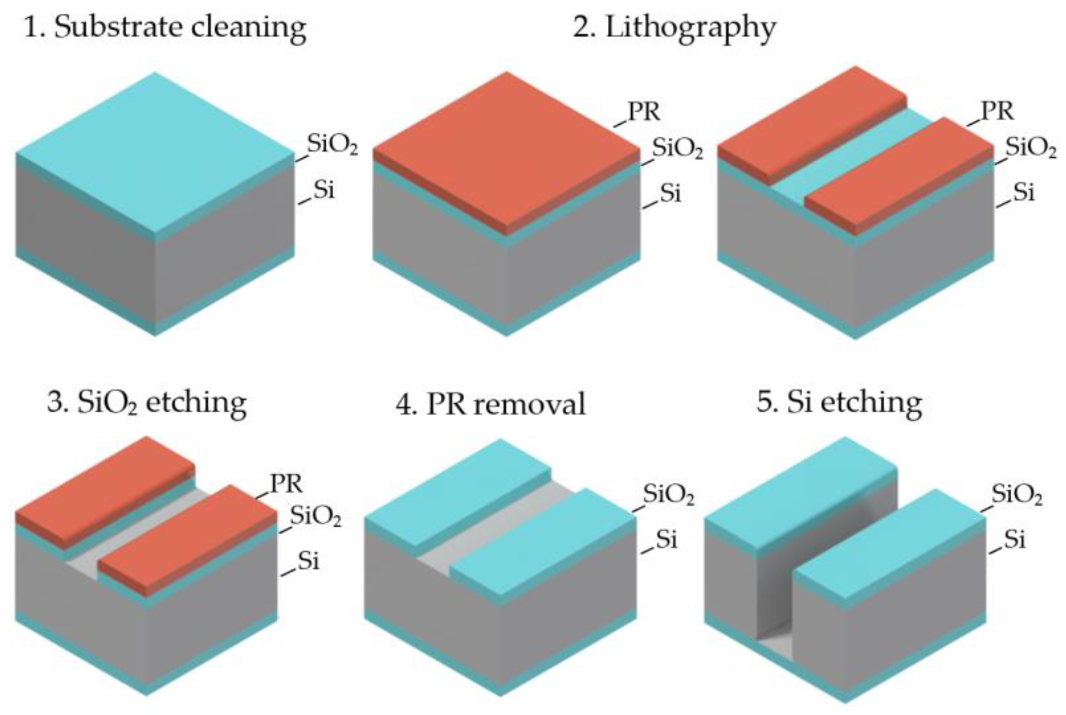
2. Materials and Methods
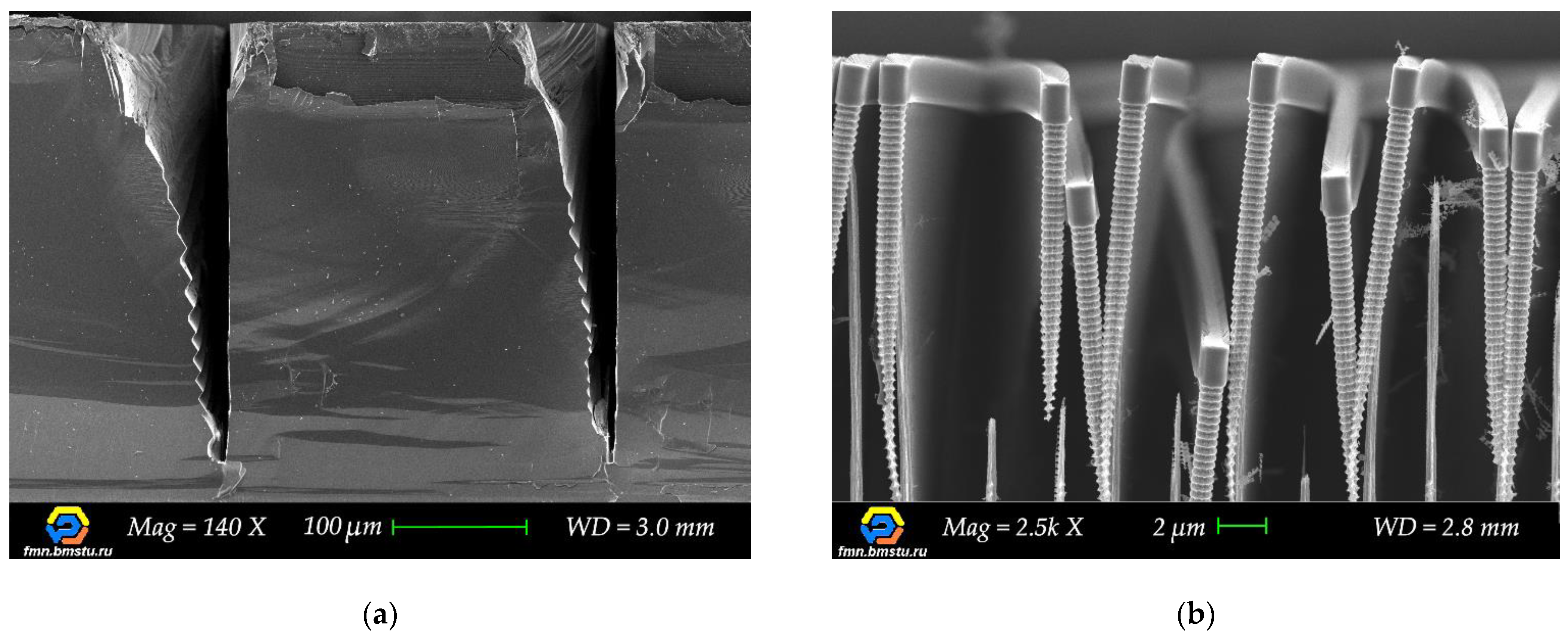
3. Results
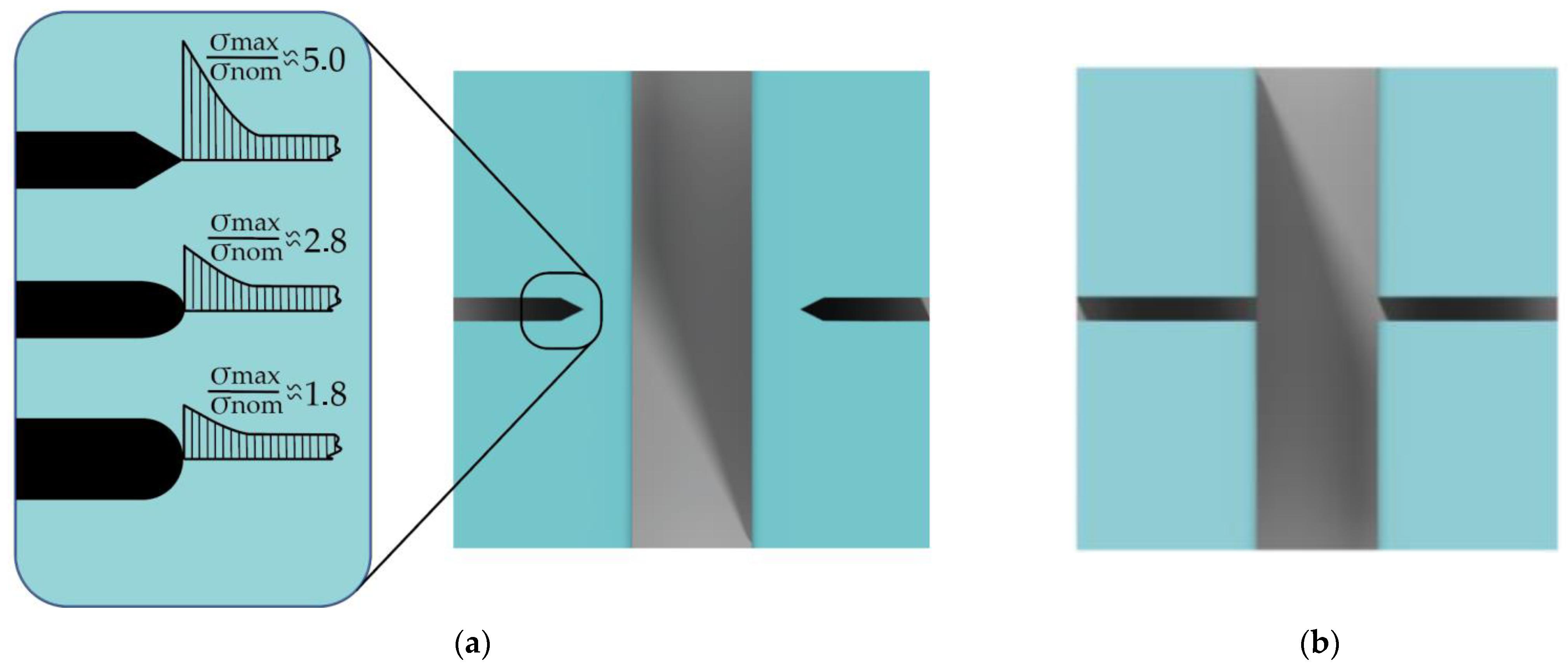
4. Discussion
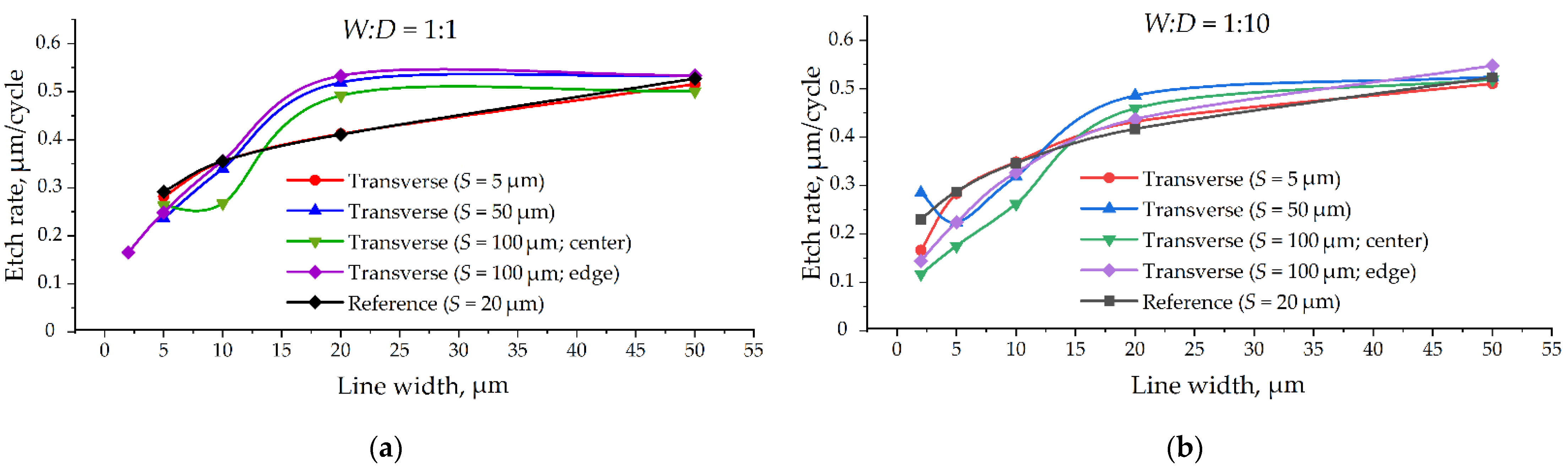
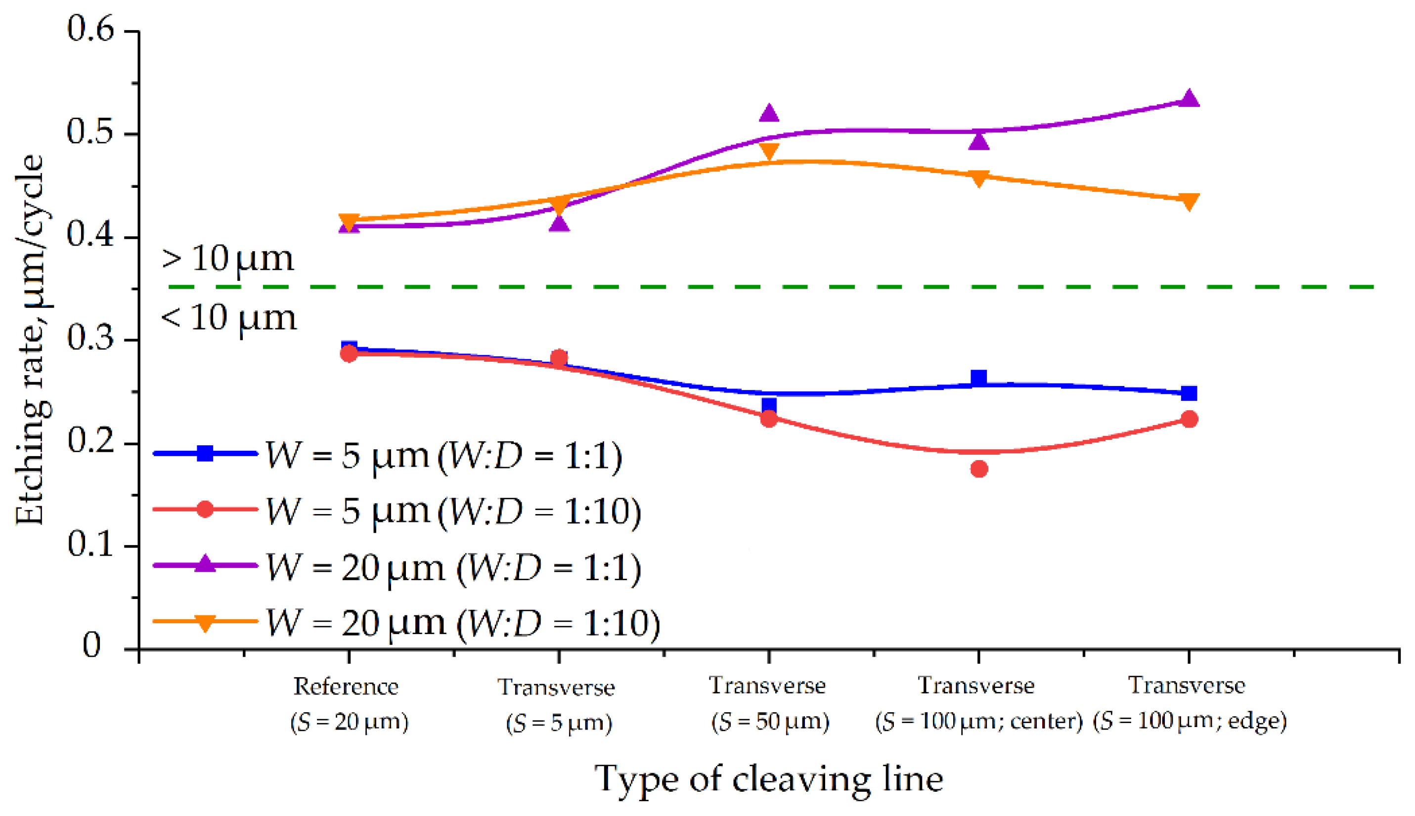
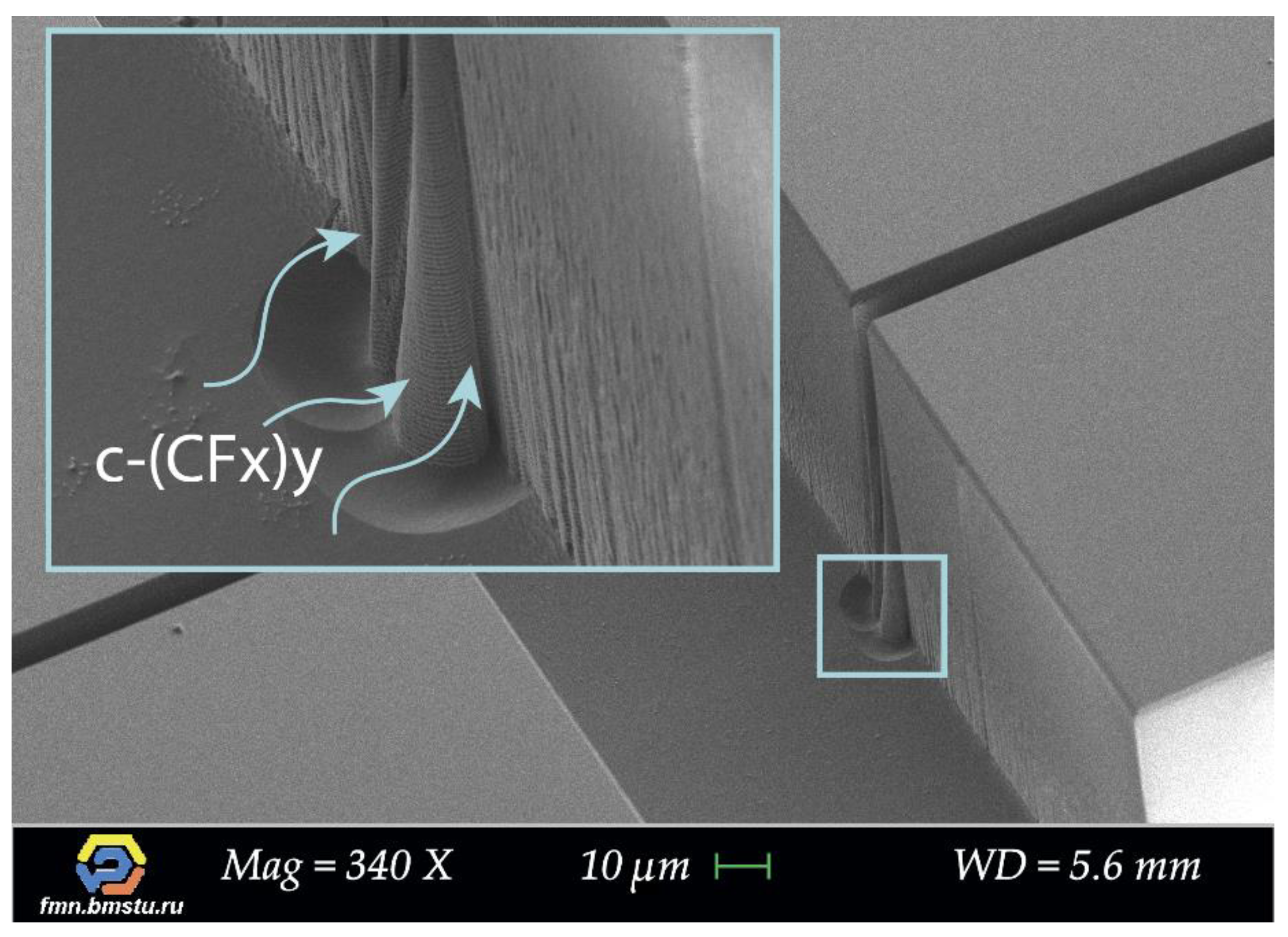
4.1. Influence of the Auxiliary Cleaving Lines on the Etching Rate
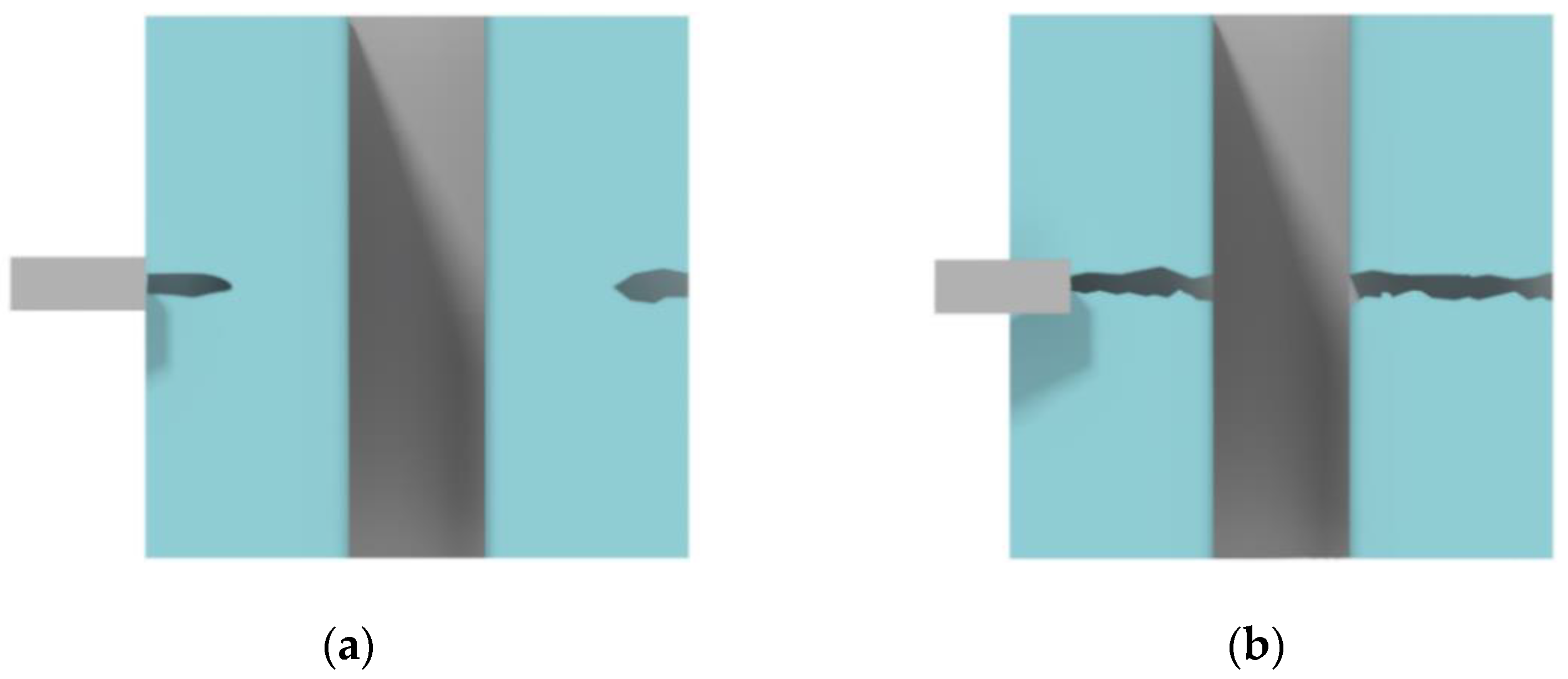
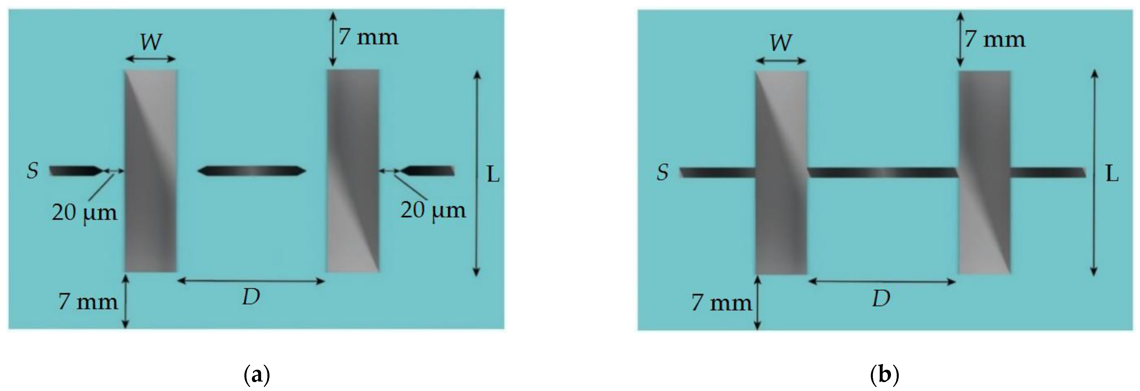
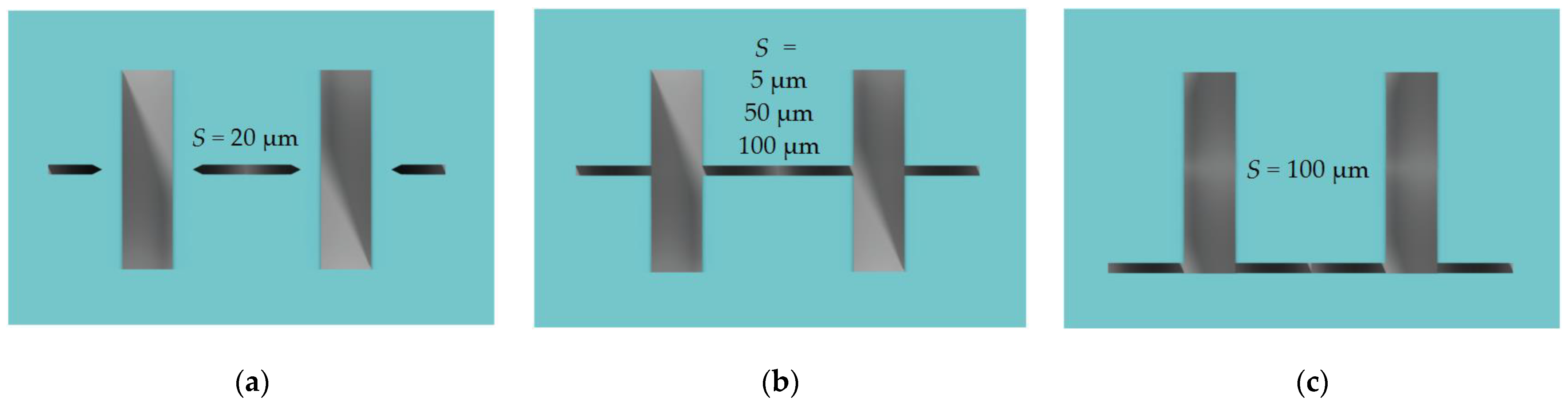
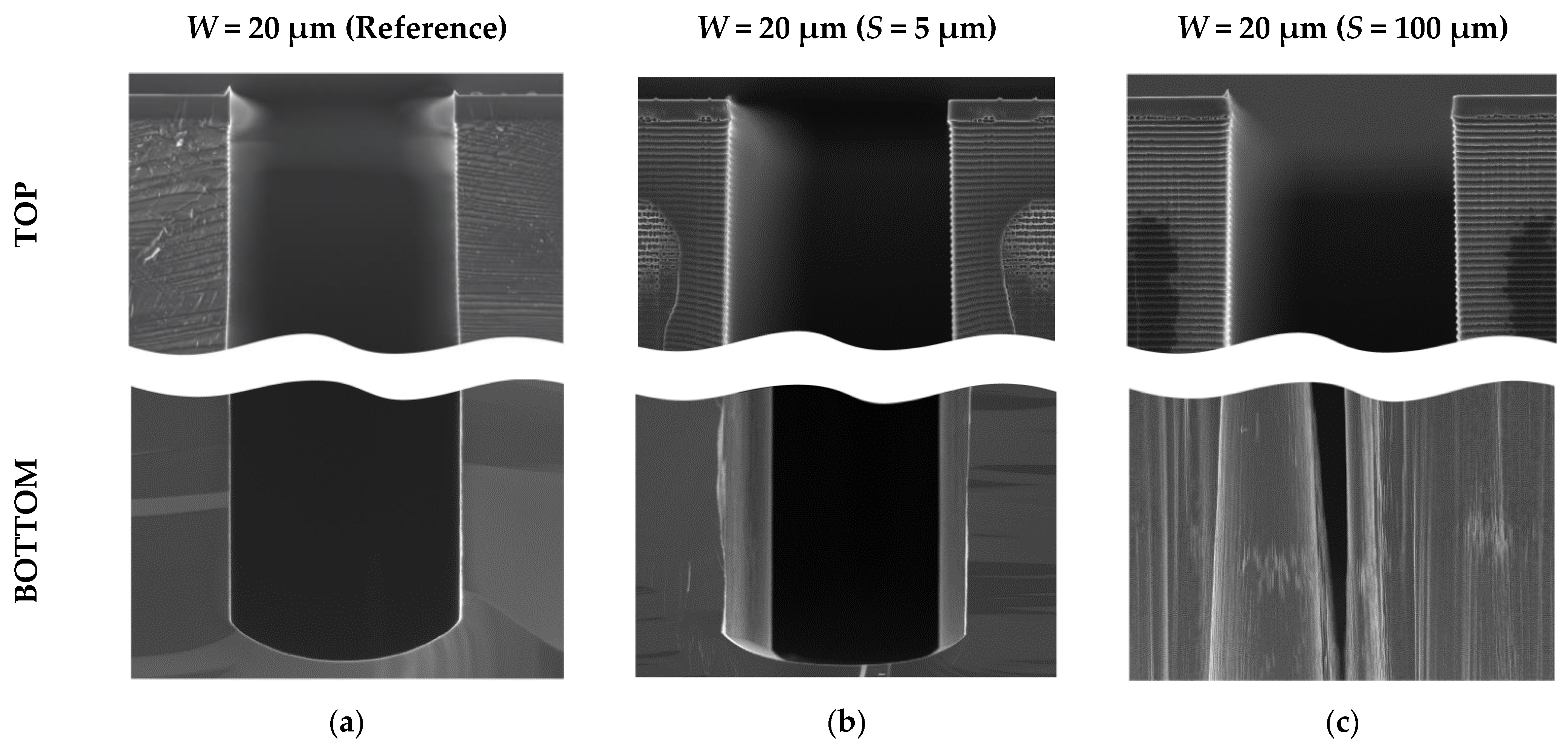
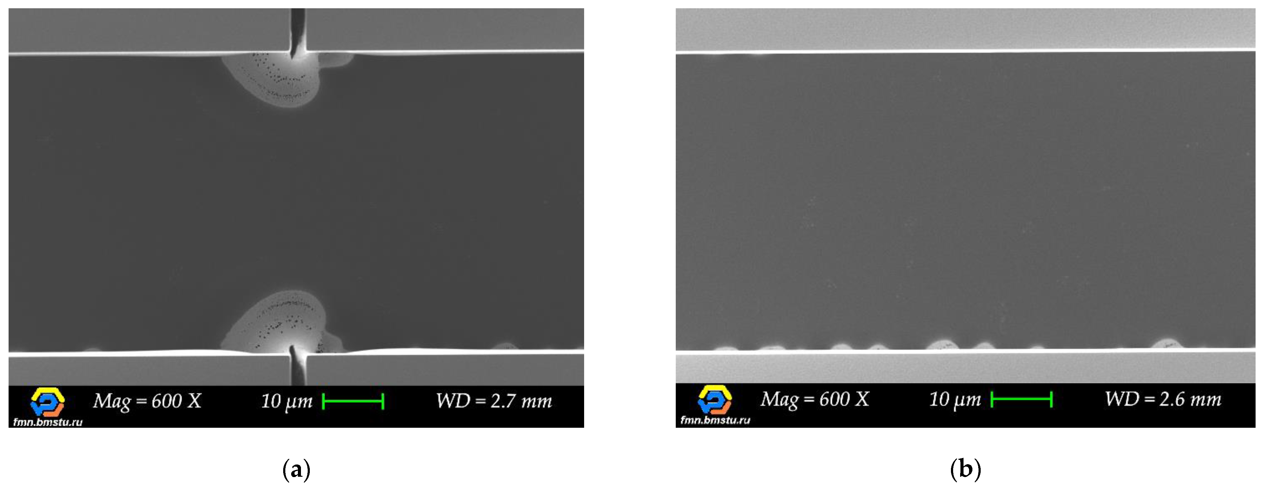
4.2. Influence of the Auxiliary Cleaving Lines on Etching Behavior
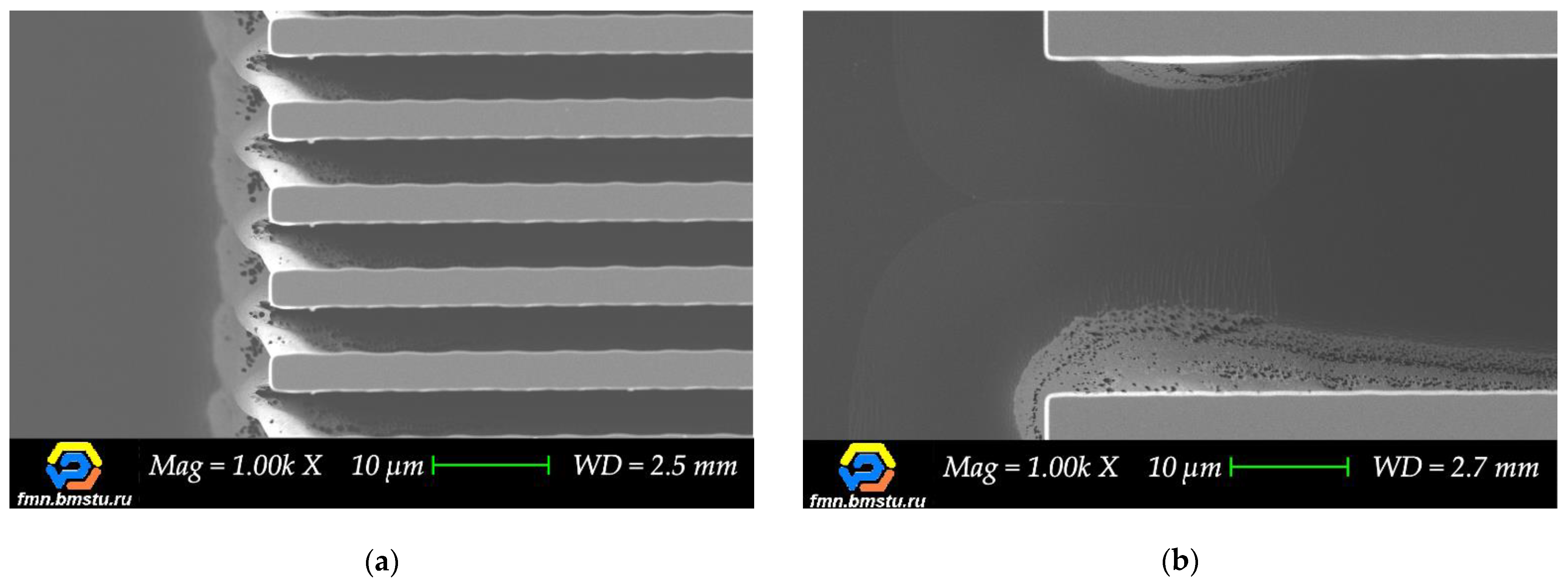
4.3. Influence of the Position of the Auxiliary Cleaving Lines
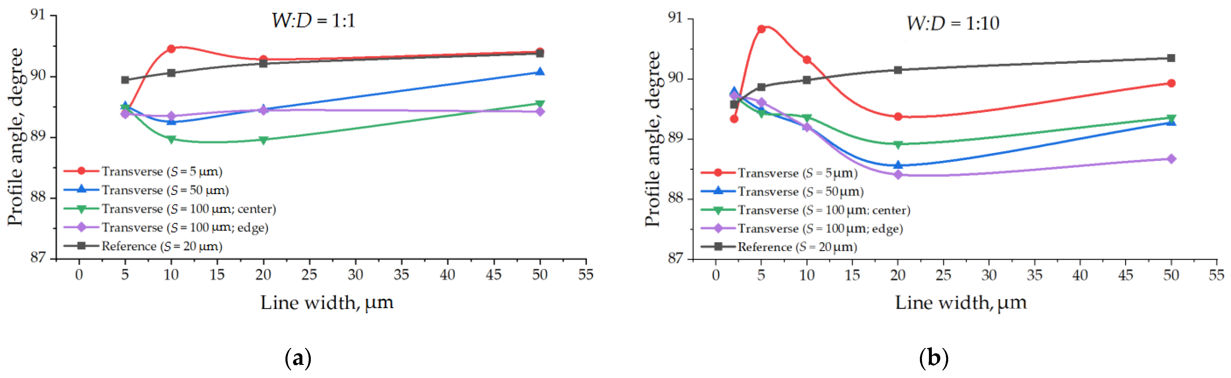
4.4. Influence of the Auxiliary Cleaving Lines on the Profile Angle
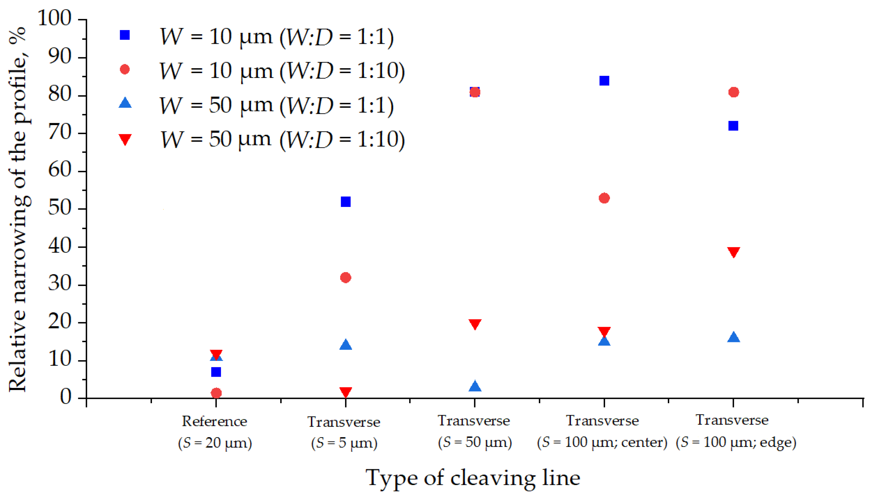
4.5. Influence of the Distance between Target Microstructures
5. Conclusions
Author Contributions
Funding
Acknowledgments
Conflicts of Interest
References
- Castañer, L. Understanding Mems: Principles and Applications; John Wiley & Sons: Hoboken, NJ, USA, 2015. [Google Scholar]
- Zhou, G.; Lee, C. Optical MEMS, Nanophotonics, and Their Applications; CRC Press: Boca Raton, FL, USA, 2017. [Google Scholar]
- Choudhary, V.; Iniewski, K.I. Mems: Fundamental Technology and Applications; CRC Press: Boca Raton, FL, USA, 2017. [Google Scholar]
- Androniс, M.M.; Rodionov, I.A.; Tsvetkov, Y.B. Digital design as a key approach to shortening MEMS development cycle. In Proceedings of the ITM Web of Conferences, Moscow, Russia, 28–29 November 2019. [Google Scholar]
- Bhardwaj, J.; Ashraf, H.; McQuarrie, A. Dry silicon etching for MEMS. Symp. Microstruct. Microfabr. Syst. 1997, 1–13. Available online: http://luxor.quantumlabs.co/home/admin/QUANTUMFAB1/PUBLICATIONS/Macropore%20Formation/dry_si_etching.pdf (accessed on 5 May 2020).
- Rangelow, I.W. Critical tasks in high aspect ratio silicon dry etching for microelectromechanical systems. J. Vac. Sci. Technol. A Vac. Surf. Films. 2003, 21, 1550–1562. [Google Scholar] [CrossRef]
- Laermer, F.; Andrea, U. MEMS at Bosch–Si plasma etch success story, history, applications, and products. Plasma Proc. Polym. 2019, 16, 1800207. [Google Scholar] [CrossRef]
- Chang, B.; Jensen, F.; Hübner, J.; Jansen, H. DREM2: A facile fabrication strategy for freestanding three dimensional silicon micro-and nanostructures by a modified Bosch etch process. J. Micromech Microeng. 2018, 28, 105012. [Google Scholar] [CrossRef]
- Westerman, R.; Martinez, L.; Pays-Volard, D.; Mackenzie, K.; Lazerand, T. Deep silicon etching: Current capabilities and future directions. Micromach. Microfabr. Proc. Technol. XIX Int. Soc. Optics Photonics 2014, 8973, 897309. [Google Scholar]
- Marty, F.; Rousseau, L.; Saadany, B.; Mercier, B.; Français, O.; Mita, Y.; Bourouina, T. Advanced etching of silicon based on deep reactive ion etching for silicon high aspect ratio microstructures and three-dimensional micro-and nanostructures. Microelectron. J. 2005, 36, 673–677. [Google Scholar] [CrossRef]
- Ranganathan, N.; Lee, D.Y.; Youhe, L.; Lo, G.Q.; Prasad, K.; Pey, K.L. Influence of Bosch etch process on electrical isolation of TSV structures. IEEE Trans. Components Packaging Manuf. Technol. 2011, 1, 1497–1507. [Google Scholar] [CrossRef]
- Gao, F.; Ylinen, S.; Kainlauri, M.; Kapulainen, M. Smooth silicon sidewall etching for waveguide structures using a modified Bosch process. J. Micro/Nanolithogr. MEMS MOEMS 2014, 13, 013010. [Google Scholar] [CrossRef]
- Fu, J.; Li, J.; Yu, J.; Liu, R.; Li, J.; Wang, W.; Chen, D. Improving sidewall roughness by combined RIE-Bosch process. Mater. Sci. Semiconduct. Process. 2018, 83, 186–191. [Google Scholar] [CrossRef]
- Mohammed, Z.A.S.; Olimpo, M.A.S.; Poenar, D.P.; Aditya, S. Smoothening of scalloped DRIE trench walls. Mater. Sci. Semiconduct. Process. 2017, 63, 83–89. [Google Scholar] [CrossRef]
- Etching, B. A Deep Silicon RIE Primer Bosch Etching of Deep Structures in Silicon. Power 2009. Available online: https://www.nanofab.ualberta.ca/wp-content/uploads/2009/03/primer_deepsiliconrie.pdf (accessed on 5 May 2021).
- Shearn, M.; Sun, X.; Henry, M.D.; Yariv, A.; Scherer, A. Advanced plasma processing: Etching, deposition, and wafer bonding techniques for semiconductor applications. In Semiconductor Technologies; Grym, J., Ed.; Intech: Rijeka, Croatia, 2010; pp. 79–104. [Google Scholar]
- Huber, R.; Conrad, J.; Schmitt, L.; Hecker, K.; Scheurer, J.; Weber, M. Fabrication of multilevel silicon structures by anisotropic deep silicon etching. Microelectron. Eng. 2003, 67, 410–416. [Google Scholar] [CrossRef]
- Bagolini, A.; Ronchin, S.; Bellutti, P.; Chistè, M.; Verotti, M.; Belfiore, N.P. Fabrication of novel MEMS microgrippers by deep reactive ion etching with metal hard mask. J. Microelectromech. Syst. 2017, 26, 926–934. [Google Scholar] [CrossRef]
- Rahiminejad, S.; Cegielski, P.; Abassi, M.; Enoksson, P. A four level silicon microstructure fabrication by DRIE. J. Micromech. Microeng. 2016, 26, 084003. [Google Scholar] [CrossRef]
- Ganji, B.A.; Majlis, B.Y. Deep trenches in silicon structure using DRIE method with aluminum as an etching mask. In Proceedings of the 2006 IEEE International Conference on Semiconductor Electronics, Kuala Lumpur, Malaysia, 29 October–1 December 2006; pp. 41–47. [Google Scholar]
- Aydinoglu, F.; Saffih, F.; Dey, R.K.; Cui, B. Chromium oxide as a hard mask material better than metallic chromium. J. Vac. Sci. Technol. B Nanotechnol. Microelectron. Mater. Process. Meas. Phenomena. 2017, 35, 06GB01. [Google Scholar] [CrossRef]
- Grigoras, K.; Sainiemi, L.; Tiilikainen, J.; Säynätjoki, A.; Airaksinen, V.; Franssila, S. Application of ultra-thin aluminum oxide etch mask made by atomic layer deposition technique. J. Physics Conf. Series IOP Publ. 2007, 61, 369. [Google Scholar] [CrossRef]
- Liu, Z.; Iltanen, K.; Chekurov, N.; Grigoras, K.; Tittonen, I. Aluminum oxide mask fabrication by focused ion beam implantation combined with wet etching. Nanotechnology 2013, 24, 175304. [Google Scholar] [CrossRef]
- Henry, M.D. Alumina etch masks for fabrication of high-aspect-ratio silicon micropillars and nanopillars. Nanotechnology 2009, 20, 255–305. [Google Scholar] [CrossRef] [PubMed]
- Hayashi, S.; Yamanaka, M.; Nakagawa, H.; Kubota, M.; Ogura, M. SiO2 etching using inductively coupled plasma. Electron. Comm. Jpn. 1998, 81, 21–29. [Google Scholar] [CrossRef]
- Alam, A.K. Etching Process Development of SiO2 Etching Using Inductively Coupled Plasma. Master’s Thesis, University of Eastern Finland, Department of Physics, Joensuu, Kuopio, Finland, 2015. [Google Scholar]
- Gaboriau, F.; Cartry, G.; Peignon, M.C.; Cardinaud, C. Selective and deep plasma etching of SiO2: Comparison between different fluorocarbon gases (CF4, C2F6, CHF3) mixed with CH4 or H2 and influence of the residence time. J. Vac. Sci. Technol. B Microelectron. Nanometer Struct. Process. Meas. Phenomena 2002, 20, 1514–1521. [Google Scholar] [CrossRef]
- Chung, C.K. Geometrical pattern effect on silicon deep etching by an inductively coupled plasma system. J. Micromech. Microeng. 2004, 14, 656. [Google Scholar] [CrossRef]
- Xu, T.; Tao, Z.; Li, H.; Tan, X.; Li, H. Effects of deep reactive ion etching parameters on etching rate and surface morphology in extremely deep silicon etch process with high aspect ratio. Adv. Mech. Eng. 2017, 9, 1687814017738152. [Google Scholar] [CrossRef]
- Yeom, J.; Wu, Y.; Selby, J.C.; Shannon, M.A. Maximum achievable aspect ratio in deep reactive ion etching of silicon due to aspect ratio dependent transport and the microloading effect. J. Vac. Sci. Technol. B Microelectron. Nanometer Struct. Process. Meas. Phenomena 2005, 23, 2319–2329. [Google Scholar] [CrossRef]
- Lai, S.; Srinivasan, S.; Westerman, R.J.; Johnson, D.; Nolan, J.J. Notch reduction in silicon on insulator (SOI) structures using a time division multiplex etch processes. In Proceedings of the MOEMS-MEMS Micro and Nanofabrication, San Jose, CA, USA, 22–27 January 2005; pp. 33–38. [Google Scholar]
- Kim, K.H.; Kim, S.C.; Park, K.Y.; Yang, S.S. DRIE fabrication of notch-free silicon structures using a novel silicon-on-patterned metal and glass wafer. J. Micromech. Microeng. 2011, 21, 045018. [Google Scholar] [CrossRef]
- Hong, P.; Guo, Z.; Yang, Z.; Yan, G. A method to reduce notching effect on the anchors of a micro-gyroscope. In Proceedings of the 6th IEEE International Conference on Nano/Micro Engineered and Molecular Systems, Kaohsiung, Taiwan, 20–23 February 2011; pp. 338–341. [Google Scholar]
- Summanwar, A.; Neuilly, F.; Bourouina, T. Elimination of notching phenomenon which occurs while performing deep silicon etching and stopping on an insulating layer. In Proceedings of the 2008 Ph.D. Research in Microelectronics and Electronics, Istanbul, Turkey, 22 June–25 April 2008; pp. 129–132. [Google Scholar]
- Jensen, S.; Hansen, O. Characterization of the microloading effect in deep reactive ion etching of silicon. Micromach. Microfabr. Process. Technol. IX Int. Soc. Optics Photonics 2003, 5342, 111–118. [Google Scholar]
- Taylor, H.K.; Sun, H.; Hill, T.F.; Farahanchi, A.; Boning, D.S. Characterizing and predicting spatial nonuniformity in the deep reactive ion etching of silicon. J. Electrochem. Soc. 2006, 153, 575. [Google Scholar] [CrossRef]
- Karttunen, J.; Kiihamaki, J.; Franssila, S. Loading effects in deep silicon etching. Micromach. Microfabr. Process. Technol. VI Int. Soc. Optics Photonics 2000, 4147, 90–97. [Google Scholar]
- Yeom, J.; Wu, Y.; Shannon, M.A. Critical aspect ratio dependence in deep reactive ion etching of silicon. In Proceedings of the 12th International Conference on Solid-State Sensors, Actuators and Microsystems. Digest of Technical Papers, Boston, MA, USA, 8–12 June 2003; pp. 1631–1634. [Google Scholar]
- Blauw, M.A. Deep Anisotropic Dry Etching of Silicon Microstructures by High-Density Plasmas, 2004. Available online: https://www.narcis.nl/publication/RecordID/oai:tudelft.nl:uuid:dbb050db-a834-47df-970e-208d6caf8bb3 (accessed on 5 May 2021).
- Tang, Y.; Sandoughsaz, A.; Owen, K.J.; Najafi, K. Ultra deep reactive ion etching of high aspect-ratio and thick silicon using a ramped-parameter process. J. Microelectromech. Syst. 2018, 27, 686–697. [Google Scholar] [CrossRef]
- Farahanchi, A. Characterization and Modeling of Pattern Dependencies and Time Evolution in Plasma Etching. Master’s Thesis, Deptartment of Electrical Engineering and Computer Science, Massachusetts Institute of Technology, Cambridge, MA, USA, June 2009. [Google Scholar]
- Slabbekoorn, J.; Schepers, B.; Gavan, K.B.; Sardo, S.; Van Huylenbroeck, S.; Vandeweyer, T.; Ranjan, M. Bosch process characterization for donut TSV’s. In Proceedings of the Eleventh International Wafer-Level Packaging Conference, San Jose, CA, USA, 11–13 November 2014. [Google Scholar]
- Lai, S.L.; Johnson, D.; Westerman, R. Aspect ratio dependent etching lag reduction in deep silicon etch processes. J. Vac. Sci. Technol. A Vac. Surf. Films 2006, 24, 1283–1288. [Google Scholar] [CrossRef]
- Abdolvand, R.; Ayazi, F. An advanced reactive ion etching process for very high aspect-ratio sub-micron wide trenches in silicon. Sens. Actuators A Phys. 2008, 144, 109–116. [Google Scholar] [CrossRef]
- Meng, L.; Yan, J. Effect of process parameters on sidewall damage in deep silicon etch. J. Micromech. Microeng. 2015, 25, 035024. [Google Scholar] [CrossRef]
- Saman, A.M.; Furumoto, T.; Ueda, T.; Hosokawa, A. A study on separating of a silicon wafer with moving laser beam by using thermal stress cleaving technique. J. Mater. Process. Technol. 2015, 223, 252–261. [Google Scholar] [CrossRef]
- Lee, J.H.; Nam-Seung, K.; Jung-Hee, L. Development of chip separation technique for InGaN-based light emitting diodes. IEEE J. Q. Electron. 2011, 47, 1493–1498. [Google Scholar]
- Haupt, O.; Schuetz, V.; Schoonderbeek, A.; Richter, L.; Kling, R. High quality laser cleaving process for mono-and polycrystalline silicon. Laser Based Micro Nanopackaging Assembly III Int. Soc. Optics Photonics 2009, 7202, 72020G. [Google Scholar]
- Figueroa, V. Designing a Mechanism to Cleave Silicon Wafers. Bachelor’s Thesis, Department of Mechanical Engineering, Massachusetts Institute of Technology, Cambridge, MA, USA, 2004. [Google Scholar]
- Volosukhin, V.A.; Logvinov, V.B.; Evtushenko, S.I. Strength of Materials: A Textbook; RIOR Publishing Center: Moscow, Russia, 1967; ISBN 978-5369011591. [Google Scholar]
- Johnson, C.W.; Johnson, D.; Martinez, L.; Plumhoff, J. Systematic approach to time division multiplexed Si etch process development. ECS Trans. 2013, 50, 11. [Google Scholar] [CrossRef]
- Saraf, I.R.; Goeckner, M.J.; Goodlin, B.E.; Kirmse, K.H.; Nelson, C.T.; Overzet, L.J. Kinetics of the deposition step in time multiplexed deep silicon etches. J. Vac. Sci. Technol. B Nanotechnol. Microelectron. Mater. Process. Meas. Phenomena 2013, 31, 011208. [Google Scholar] [CrossRef]
- Labelle, C.B.; Donnelly, V.M.; Bogart, G.R.; Opila, R.L.; Kornblit, A. Investigation of fluorocarbon plasma deposition from c-C 4 F 8 for use as passivation during deep silicon etching. J. Vac. Sci. Technol. A Vac. Surf. Films 2004, 22, 2500–2507. [Google Scholar]


| Step | Inductively Coupled Plasma (ICP) (W) | Radiofrequency (RF) (W) | Pressure (mTorr) | Process Gases |
|---|---|---|---|---|
| Passivation | 1200–1500 | 5 | 20 | C4F8/SF6/O2 mixture |
| Breakthrough | 50 | 30 | ||
| Etching | 5 | 40 |
| Type of Cleaving Lines | Cleaving Lines Width (S), μm | Target Line Width (W), μm | Target Line Length (L), μm | ||||||
|---|---|---|---|---|---|---|---|---|---|
| Dashed auxiliary lines | 20 | 2 | 5 | 10 | 20 | 50 | 1000 | ||
| Transverse crossing auxiliary lines | 5 | 50 | 100 | ||||||
| Type of Cleaving Auxiliary Lines | Process Parameter | Target Lines Width | ||||
|---|---|---|---|---|---|---|
| 2 μm * | 5 μm | 10 μm | 20 μm | 50 μm | ||
| Dashed auxiliary lines (Reference) (S = 20 μm) | V, μm/cycle | - | 0.292 | 0.356 | 0.411 | 0.527 |
| Selectivity | - | 126 | 154 | 178 | 243 | |
| A, degree | - | 89.94 | 90.06 | 90.21 | 90.38 | |
| Transverse auxiliary lines (S = 5 μm) | V, μm/cycle | - | 0.282 | 0.355 | 0.412 | 0.516 |
| Selectivity | - | 122 | 153 | 178 | 223 | |
| A, degree | - | 89.39 | 90.45 | 90.28 | 90.41 | |
| Transverse auxiliary lines (S = 50 μm) | V, μm/cycle | - | 0.237 | 0.340 | 0.519 | 0.533 |
| Selectivity | - | 102 | 147 | 225 | 231 | |
| A, degree | - | 89.51 | 89.26 | 89.46 | 90.07 | |
| Transverse auxiliary lines (S = 100 μm, center) | V, μm/cycle | - | 0.263 | 0.268 | 0.492 | 0.501 |
| Selectivity | - | 114 | 116 | 213 | 217 | |
| A, degree | - | 89.49 | 88.98 | 88.96 | 89.56 | |
| Transverse auxiliary lines (S = 100 μm, edge) | V, μm/cycle | 0.165 | 0.249 | 0.356 | 0.533 | 0.534 |
| Selectivity | 72 | 108 | 154 | 231 | 231 | |
| A, degree | - | 89.38 | 89.35 | 89.44 | 89.43 | |
| Type of Cleaving Line | Process Parameter | Target Lines Width | ||||
|---|---|---|---|---|---|---|
| 2 μm | 5 μm | 10 μm | 20 μm | 50 μm | ||
| Dashed auxiliary lines (Reference) (S = 20 μm) | V, μm/cycle | 0.230 | 0.287 | 0.346 | 0.417 | 0.523 |
| Selectivity | 93 | 116 | 140 | 168 | 211 | |
| A, degree | 89.58 | 89.87 | 89.98 | 90.15 | 90.35 | |
| Transverse auxiliary lines (S = 5 μm) | V, μm/cycle | 0.167 | 0.283 | 0.349 | 0.432 | 0.510 |
| Selectivity | 72 | 123 | 151 | 187 | 221 | |
| A, degree | 89.34 | 90.83 | 90.32 | 89.38 | 89.93 | |
| Transverse auxiliary lines (S = 50 μm) | V, μm/cycle | 0.285 | 0.224 | 0.319 | 0.486 | 0.524 |
| Selectivity | 123 | 97 | 138 | 210 | 227 | |
| A, degree | 89.80 | 89.49 | 89.20 | 88.57 | 89.28 | |
| Transverse auxiliary lines (S = 100 μm, center) | V, μm/cycle | 0.117 | 0.175 | 0.262 | 0.459 | 0.519 |
| Selectivity | 51 | 76 | 113 | 199 | 225 | |
| A, degree | 89.72 | 89.44 | 89.36 | 88.92 | 89.36 | |
| Transverse auxiliary lines (S = 100 μm, edge) | V, μm/cycle | 0.145 | 0.224 | 0.327 | 0.437 | 0.548 |
| Selectivity | 63 | 97 | 141 | 189 | 237 | |
| A, degree | 89.72 | 89.61 | 89.20 | 88.41 | 88.68 | |
Publisher’s Note: MDPI stays neutral with regard to jurisdictional claims in published maps and institutional affiliations. |
© 2021 by the authors. Licensee MDPI, Basel, Switzerland. This article is an open access article distributed under the terms and conditions of the Creative Commons Attribution (CC BY) license (https://creativecommons.org/licenses/by/4.0/).
Share and Cite
Baklykov, D.A.; Andronic, M.; Sorokina, O.S.; Avdeev, S.S.; Buzaverov, K.A.; Ryzhikov, I.A.; Rodionov, I.A. Self-Controlled Cleaving Method for Silicon DRIE Process Cross-Section Characterization. Micromachines 2021, 12, 534. https://doi.org/10.3390/mi12050534
Baklykov DA, Andronic M, Sorokina OS, Avdeev SS, Buzaverov KA, Ryzhikov IA, Rodionov IA. Self-Controlled Cleaving Method for Silicon DRIE Process Cross-Section Characterization. Micromachines. 2021; 12(5):534. https://doi.org/10.3390/mi12050534
Chicago/Turabian StyleBaklykov, Dmitry A., Mihail Andronic, Olga S. Sorokina, Sergey S. Avdeev, Kirill A. Buzaverov, Ilya A. Ryzhikov, and Ilya A. Rodionov. 2021. "Self-Controlled Cleaving Method for Silicon DRIE Process Cross-Section Characterization" Micromachines 12, no. 5: 534. https://doi.org/10.3390/mi12050534
APA StyleBaklykov, D. A., Andronic, M., Sorokina, O. S., Avdeev, S. S., Buzaverov, K. A., Ryzhikov, I. A., & Rodionov, I. A. (2021). Self-Controlled Cleaving Method for Silicon DRIE Process Cross-Section Characterization. Micromachines, 12(5), 534. https://doi.org/10.3390/mi12050534