
Wafer-Level 3D Integration Based on Poly (Diallyl Phthalate) Adhesive Bonding


Abstract
:1. Introduction
2. Materials and Experiment Methods
2.1. 3D Integration Materials
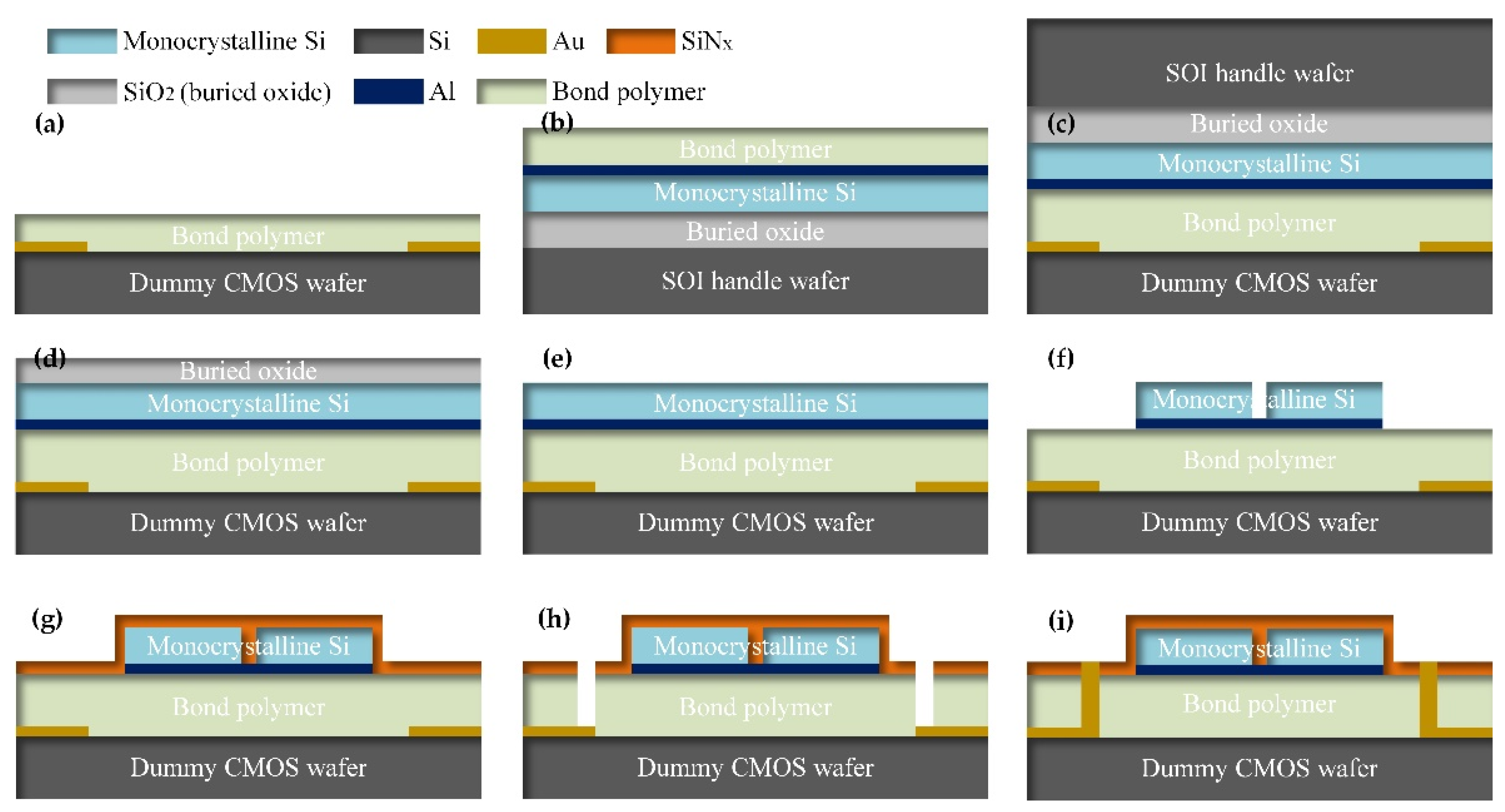
2.2. 3D-Integration Procedure
- First, clean the wafers in a standard acetone–isopropanol clean procedure (acetone ultrasonic cleaning 10 min, isopropanol ultrasonic cleaning 10 min, and deionized water rinse 2 min) and blow dry the wafers with N2. The wafers should then be baked in a vacuum oven at temperatures higher than 100 °C for 1 h in order to completely remove any remaining moisture.
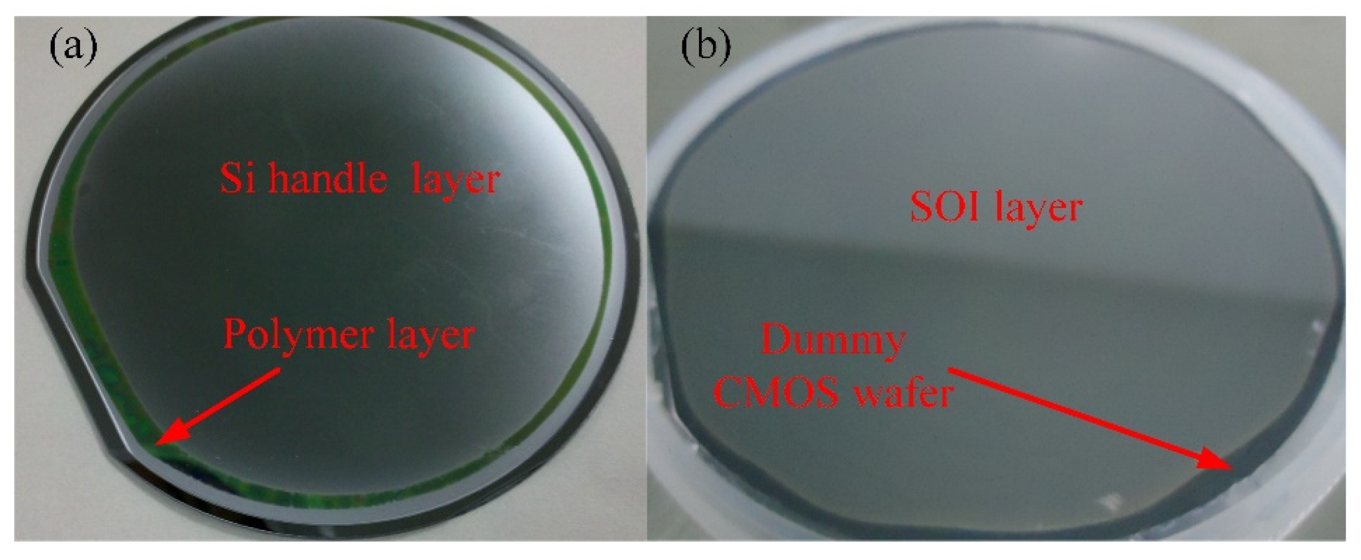
- Second, the adhesive polymer is spin-coasted on the wafer surfaces in order for it to be bonded (as shown in Figure 1a,b). Then, the polymer-coated wafers are baked and pre-cured on a hot plate for a few minutes in order to remove the solvent in the polymer, making the polymer become partially crosslinked. In addition, oxygen plasma treatment is an option step that can be implemented after pre-curing to create a stronger bond.
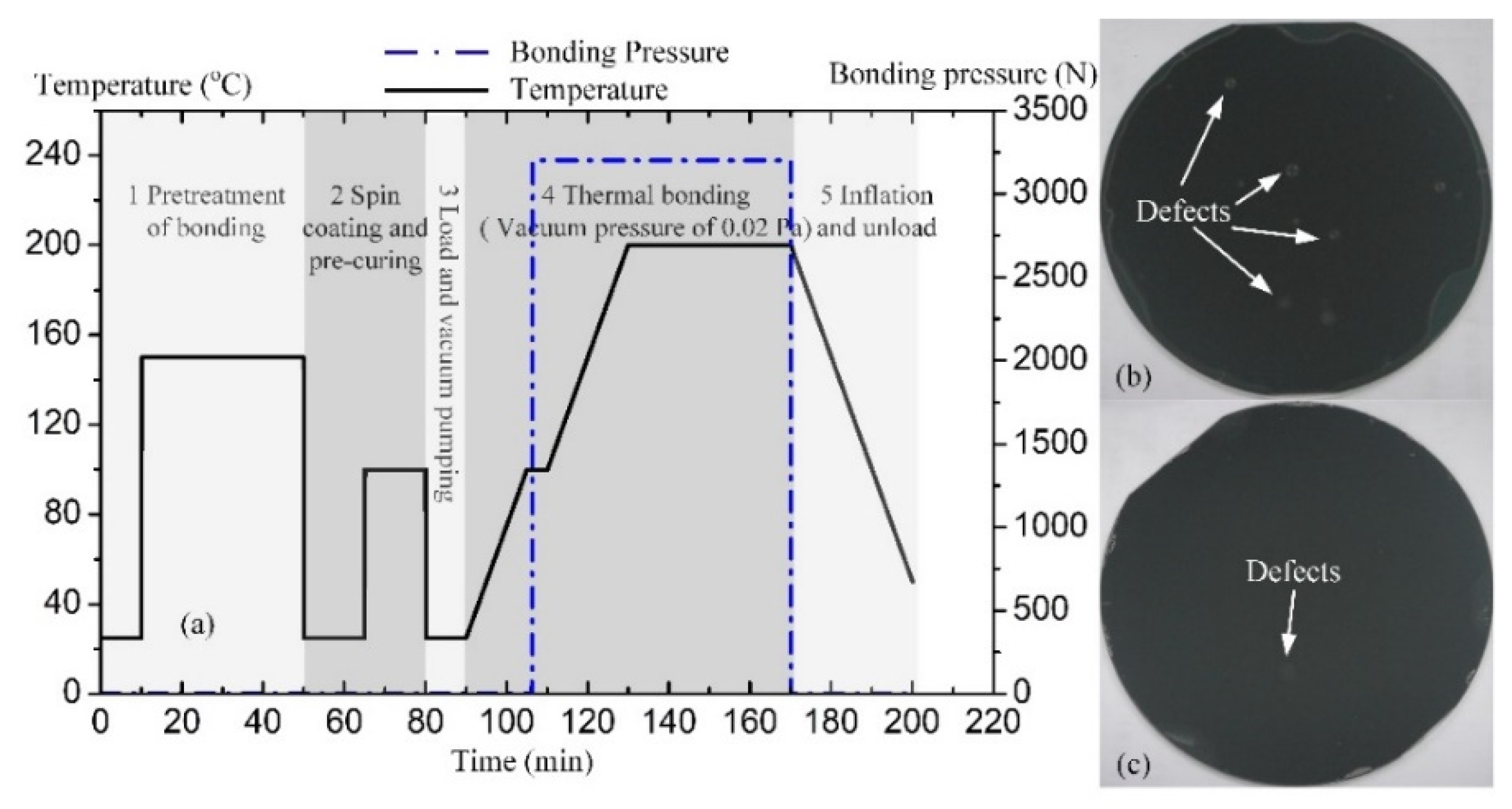
- Third, the wafers are placed in a bonder fixture so that they can be manually aligned, a process that is conducted by clamping with a BA6 aligner. The pair of wafers are separated by three bonder fixture spacers. After that, the fixture with the wafer pairs is moved into the CB6L bonder chamber, which is then closed and sealed. The chamber is pumped to a pressure of less than 0.02 Pa, and this pressure is maintained for 5 min.
- Forth, the spacers should be removed, which can be achieved using the drive mechanism of the bonder, and the wafers will then be in contact with each other. Then, bonding pressure is applied to the backside of wafers by up-pressing chuck and down-pressing chuck. After that, the wafers are heated to the polymer-curing temperature with a temperature ramping speed of 5 °C/min, which is carried out using the hot plate within the up-pressing chuck and the down-pressing chuck. The curing temperature should be maintained for 40 min in order to ensure that the polymer is completely cross-linked. The temperature of the plate should then be decreased to 40 °C by blowing N2 with a temperature speed of about 5 °C/min.
- Finally, the bonder chamber is inflated to atmospheric pressure, and the bonding pressure is unloaded. The wafer pair should be removed from the chamber, and at this point, adhesive wafer bonding has been achieved (as shown in Figure 1c).
3. Results and Discussion
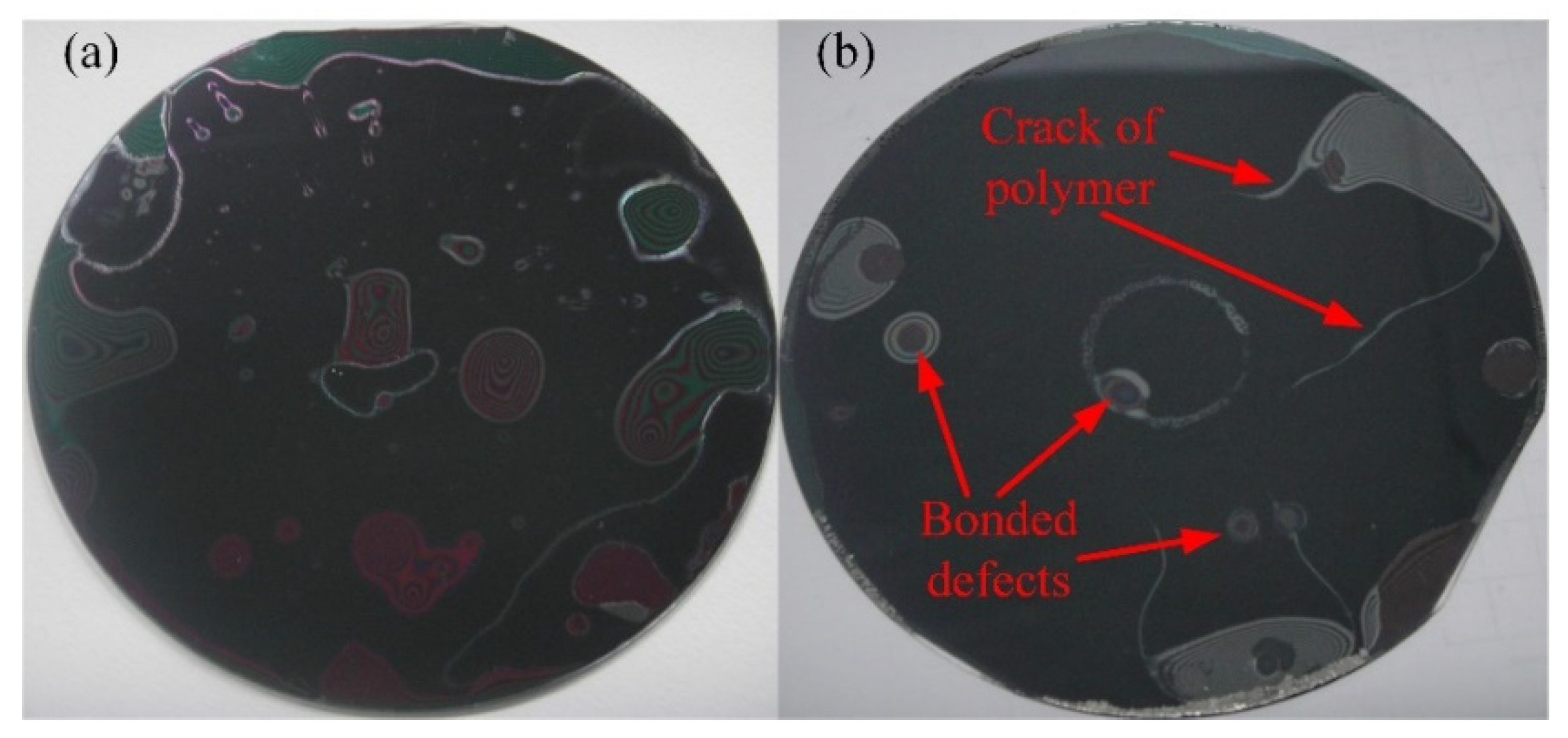
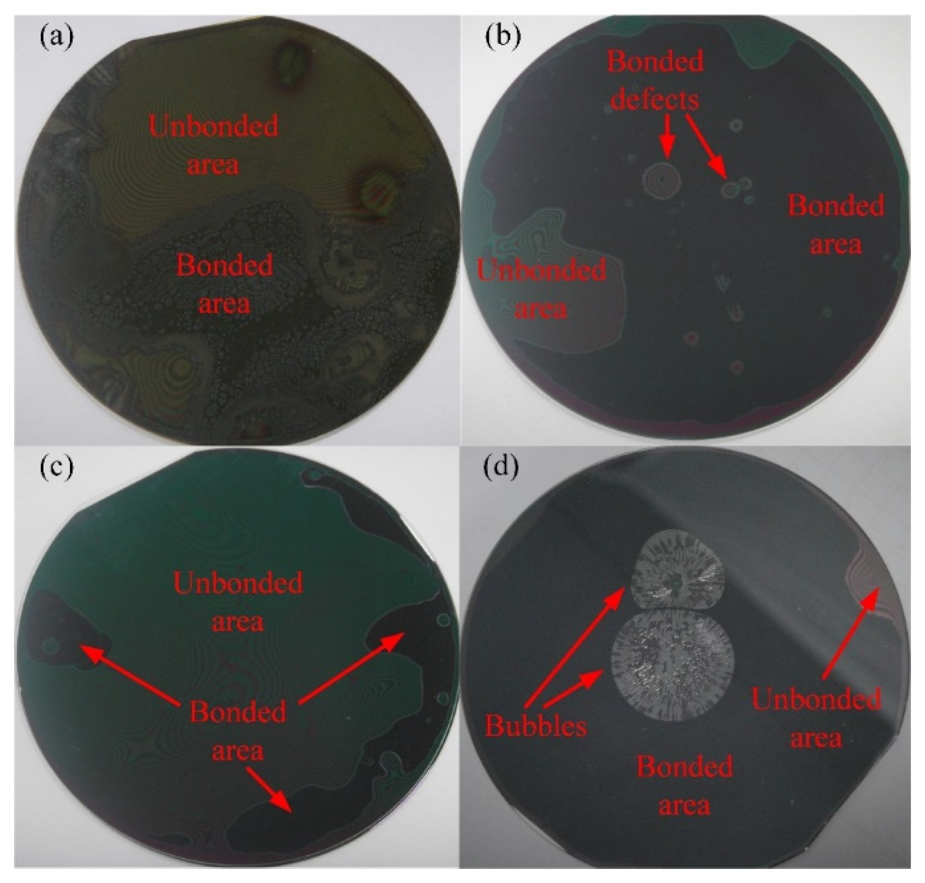
3.1. Adhesive Wafer Bonding Results and Analysis
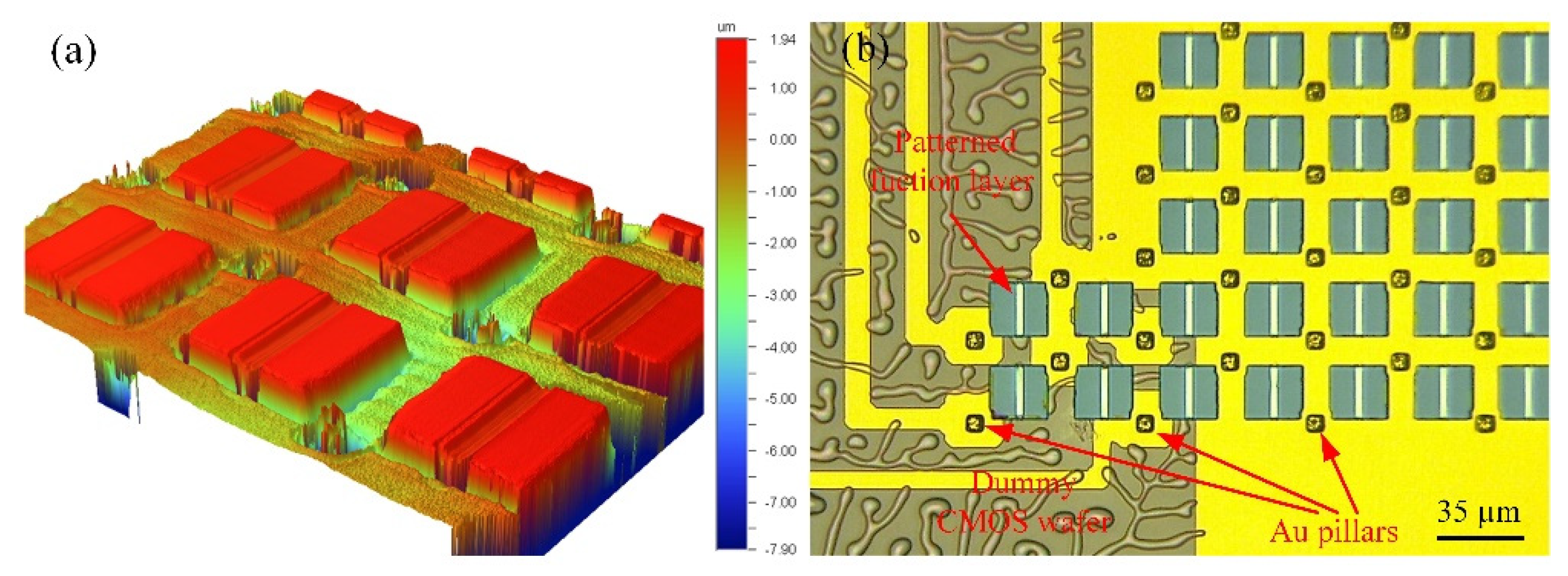
3.2. 3D Integration Results and Applications
4. Conclusions
Author Contributions
Funding
Conflicts of Interest
References
- Ko, C.T.; Chen, K.N. Low temperature bonding technology for 3D integration. Microelectron. Reliab. 2012, 52, 302–311. [Google Scholar] [CrossRef]
- Jiang, J.; Parto, K.; Cao, W.; Banerjee, K. Ultimate monolithic-3D integration with 2D materials: Rationale, prospects, and challenges. IEEE J. Electron. Devices Soc. 2019, 7, 878–887. [Google Scholar] [CrossRef]
- Koester, S.J.; Young, A.M.; Yu, R.R.; Purushothaman, S.; Chen, K.N.; La Tulipe, D.C.; Rana, N.; Shi, L.; Wordeman, M.R.; Sprogis, E.J. Wafer-level 3D integration technology. IBM J. Res. Dev. 2008, 52, 583–597. [Google Scholar] [CrossRef]
- Koyanagi, M. Recent progress in 3D integration technology. IEICE Electron. Express 2015, 12, 20152001. [Google Scholar] [CrossRef] [Green Version]
- Reda, S. 3D integration advances computing. Nature 2017, 547, 38–39. [Google Scholar] [CrossRef] [PubMed]
- Kim, S.E.; Kim, S. Wafer level Cu–Cu direct bonding for 3D integration. Microelectron. Eng. 2015, 137, 158–163. [Google Scholar] [CrossRef]
- Higurashi, E.; Suga, T. Review of low-temperature bonding technologies and their application in optoelectronic devices. Electron. Commun. Jpn. 2016, 99, 63–71. [Google Scholar] [CrossRef]
- Higurashi, E. Low-temperature bonding technologies for photonics applications. ECS Trans. 2013, 50, 351. [Google Scholar] [CrossRef]
- Niklaus, F.; Stemme, G.; Lu, J.Q.; Gutmann, R.J. Adhesive wafer bonding. J. Appl. Phys. 2006, 99, 2. [Google Scholar] [CrossRef]
- Niklaus, F.; Kumar, R.J.; McMahon, J.J.; Yu, J.; Lu, J.Q.; Cale, T.S.; Gutmann, R.J. Adhesive wafer bonding using partially cured benzocyclobutene for three-dimensional integration. J. Electrochem. Soc. 2006, 153, G291. [Google Scholar] [CrossRef]
- Forsberg, F.; Lapadatu, A.; Kittilsland, G.; Martinsen, S.; Roxhed, N.; Fischer, A.C.; Stemme, G.; Samel, B.; Ericsson, P.; Høivik, N.; et al. CMOS-integrated Si/SiGe quantum-well infrared microbolometer focal plane arrays manufactured with very large-scale heterogeneous 3-D integration. IEEE J. Sel. Top. Quantum Electron. 2015, 21, 30–40. [Google Scholar] [CrossRef] [Green Version]
- Niklaus, F.; Kälvesten, E.; Stemme, G. Wafer-level membrane transfer bonding of polycrystalline silicon bolometers for use in infrared focal plane arrays. J. Micromech. Microeng. 2001, 11, 509. [Google Scholar] [CrossRef]
- Zimmer, F.; Lapisa, M.; Bakke, T.; Bring, M.; Stemme, G.; Niklaus, F. One-megapixel monocrystalline-silicon micromirror array on CMOS driving electronics manufactured with very large-scale heterogeneous integration. J. Microelectromech. Syst. 2011, 20, 564–572. [Google Scholar] [CrossRef]
- Schmidt, J.U.; Friedrichs, M.; Bakke, T.; Voelker, B.; Rudloff, D.; Lakner, H. Technology development for micromirror arrays with high optical fill factor and stable analogue deflection integrated on CMOS substrates. In Proceedings of the MEMS, MOEMS, and Micromachining III, International Society for Optics and Photonics, Strasbourg, France, 25 April 2008; p. 69930D. [Google Scholar]
- Guerre, R.; Drechsler, U.; Bhattacharyya, D.; Rantakari, P.; Stutz, R.; Wright, R.V.; Milosavljevic, Z.D.; Vaha, H.T.; Kirby, P.B.; Despont, M. Wafer-level transfer technologies for PZT-based RF MEMS switches. J. Microelectromech. Syst. 2010, 19, 548–560. [Google Scholar] [CrossRef]
- Makihata, M.; Tanaka, S.; Muroyama, M.; Matsuzaki, S.; Yamada, H.; Nakayama, T.; Yamaguchi, U.; Mima, K.; Nonomura, Y.; Esashi, M. Adhesive wafer bonding using a molded thick benzocyclobutene layer for wafer-level integration of MEMS and LSI. J. Micromech. Microeng. 2011, 21, 085002. [Google Scholar] [CrossRef]
- Agirregabiria, M.; Blanco, F.J.; Berganzo, J.; Arroyo, M.T.; Fullaondo, A.; Mayora, K.; Ruano-Lopez, J.M. Fabrication of SU-8 multilayer microstructures based on successive CMOS compatible adhesive bonding and releasing steps. Lab Chip 2005, 5, 545–552. [Google Scholar] [CrossRef] [PubMed]
- Bleiker, S.J.; Dubois, V.; Schröder, S.; Stemme, G.; Niklaus, F. Adhesive wafer bonding with ultra-thin intermediate polymer layers. Sens. Actuators A Phys. 2017, 260, 16–23. [Google Scholar] [CrossRef]
- Niklaus, F.; Decharat, A.; Forsberg, F.; Roxhed, N.; Lapisa, M.; Populin, M.; Stemme, G. Wafer bonding with nano-imprint resists as sacrificial adhesive for fabrication of silicon-on-integrated-circuit (SOIC) wafers in 3D integration of MEMS and ICs. Sens. Actuators A Phys. 2009, 154, 180–186. [Google Scholar] [CrossRef]
- Micro Resist Technology. Available online: https://www.microresist.de/ (accessed on 17 October 2016).
- Zhong, F.; Dong, T.; Yong, H.; Yan, S.; Wang, K. Void-free wafer-level adhesive bonding utilizing modified poly (diallyl phthalate). J. Micromech. Microeng. 2013, 23, 125021. [Google Scholar] [CrossRef]
- Giurlani, W.; Zangari, G.; Gambinossi, F.; Passaponti, M.; Salvietti, E.; Di Benedetto, F.; Caporali, S.; Innocenti, M. Electroplating for decorative applications: Recent trends in research and development. Coatings 2018, 8, 260. [Google Scholar] [CrossRef] [Green Version]


| Material | Curing Temperature (°C) | Thickness @ 3000 rpm | Thermal Stability (°C) |
|---|---|---|---|
| MR-I 9100M | 150–225 | 1000 nm | 260 |
| MR-I 9150XP | 150–225 | 1500 nm | 260 |
| MA-N 1410 | 100–120 | 1000 nm | 160 |
| Metal | γ (g/cm3) | v (nm/min) | K (g/Ah) | η | De (A/dm2) | Se (dm2) | I (mA) |
|---|---|---|---|---|---|---|---|
| Au | 19.3 | 150 | 7.349 | 0.95 | 0.249 | 0.04 | 10 |
| Cu | 8.93 | 100 | 1.186 | 0.95 | 0.476 | 0.04 | 19 |
| No | Label | RPM | Pre-Curing Temperature (°C) | Pre-Curing Time (min) | Bonding Pressure (N) | Bonding Temperature (°C) |
|---|---|---|---|---|---|---|
| 1 | MA-N 1410 | 3000 | 100 | 3 | 1500 | 120 |
| 2 | MR-I 9100M | 1330 | 100 | 15 | 1500 | 200 |
| 3 | MR-I 9150XP | 3000 | 150 | 15 | 1500 | 200 |
| 4 | MR-I 9100M | 1330 | 100 | 5 | 3200 | 200 |
| 5 | MR-I 9100M 1 | 3000 | 100 | 10 | 3200 | 200 |
| 6 | MR-I 9150XP 2 | 3000 | 100 | 5 | 3200 | 200 |
| 7 | MR-I 9100M | 3000 | 100 | 15 | 3200 | 200 |
| 8 | MR-I 9150XP | 3000 | 100 | 15 | 3200 | 200 |
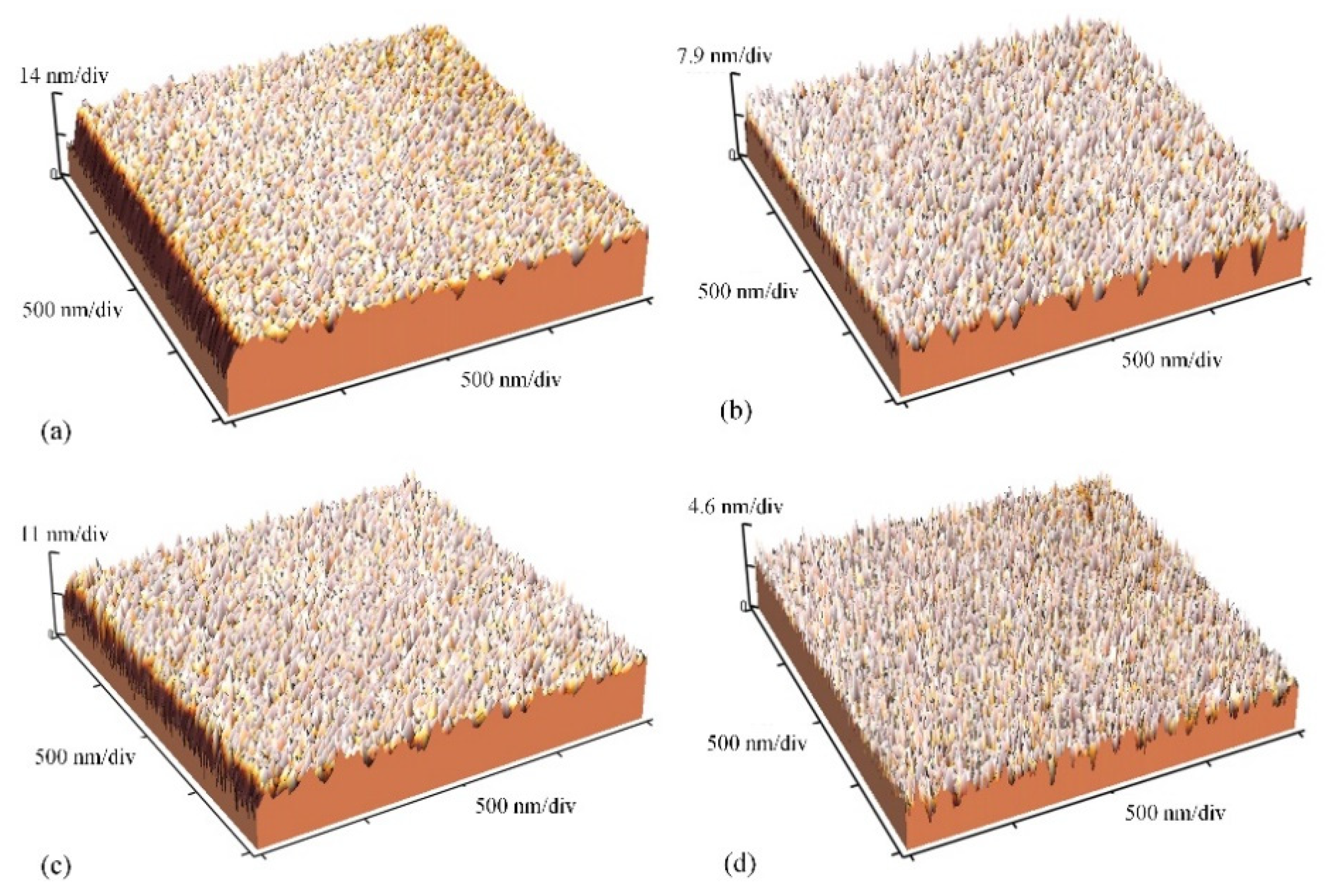
| Label | Ra (nm) | Rz (nm) | Rt (nm) | Rq (nm) |
|---|---|---|---|---|
| Figure 5a | 1.85 | 27.43 | 20.27 | 2.75 |
| Figure 5b | 1.33 | 13.55 | 8.96 | 1.66 |
| Figure 5c | 1.73 | 21.13 | 13.42 | 2.25 |
| Figure 5d | 0.86 | 9.28 | 4.33 | 1.08 |
| No | Background Vacuum Degree | RF Power | Reaction Gas Ration (sccm) | Assistant Gas Ration (sccm) | Reaction Pressure | Etch Rate (nm/min) |
|---|---|---|---|---|---|---|
| 1 | 0.002 Pa | 200 W | 40 | 0 | 2.66 Pa | 410 |
| 2 | 0.005 Pa | 200 W | 40 | 10 | 3.99 Pa | 580 |
Publisher’s Note: MDPI stays neutral with regard to jurisdictional claims in published maps and institutional affiliations. |
© 2021 by the authors. Licensee MDPI, Basel, Switzerland. This article is an open access article distributed under the terms and conditions of the Creative Commons Attribution (CC BY) license (https://creativecommons.org/licenses/by/4.0/).
Share and Cite
Fang, Z.; You, P.; Jia, Y.; Pan, X.; Shi, Y.; Jiao, J.; He, Y. Wafer-Level 3D Integration Based on Poly (Diallyl Phthalate) Adhesive Bonding. Micromachines 2021, 12, 1586. https://doi.org/10.3390/mi12121586
Fang Z, You P, Jia Y, Pan X, Shi Y, Jiao J, He Y. Wafer-Level 3D Integration Based on Poly (Diallyl Phthalate) Adhesive Bonding. Micromachines. 2021; 12(12):1586. https://doi.org/10.3390/mi12121586
Chicago/Turabian StyleFang, Zhong, Peng You, Yijie Jia, Xuchao Pan, Yunlei Shi, Junjie Jiao, and Yong He. 2021. "Wafer-Level 3D Integration Based on Poly (Diallyl Phthalate) Adhesive Bonding" Micromachines 12, no. 12: 1586. https://doi.org/10.3390/mi12121586
APA StyleFang, Z., You, P., Jia, Y., Pan, X., Shi, Y., Jiao, J., & He, Y. (2021). Wafer-Level 3D Integration Based on Poly (Diallyl Phthalate) Adhesive Bonding. Micromachines, 12(12), 1586. https://doi.org/10.3390/mi12121586