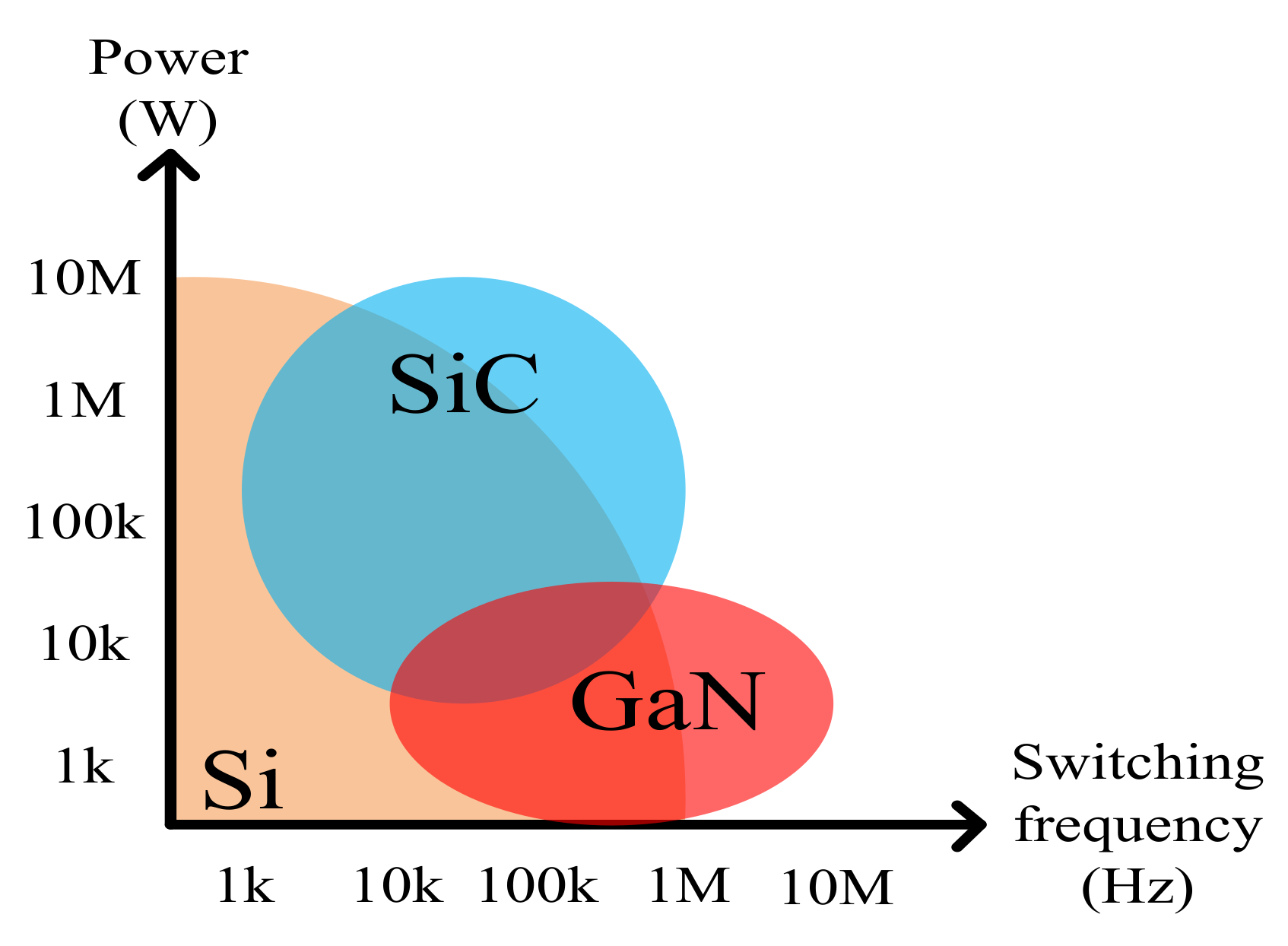
Figure 1.
Comparison of Si, gallium nitride (GaN), and silicon carbide (SiC).
Figure 1.
Comparison of Si, gallium nitride (GaN), and silicon carbide (SiC).
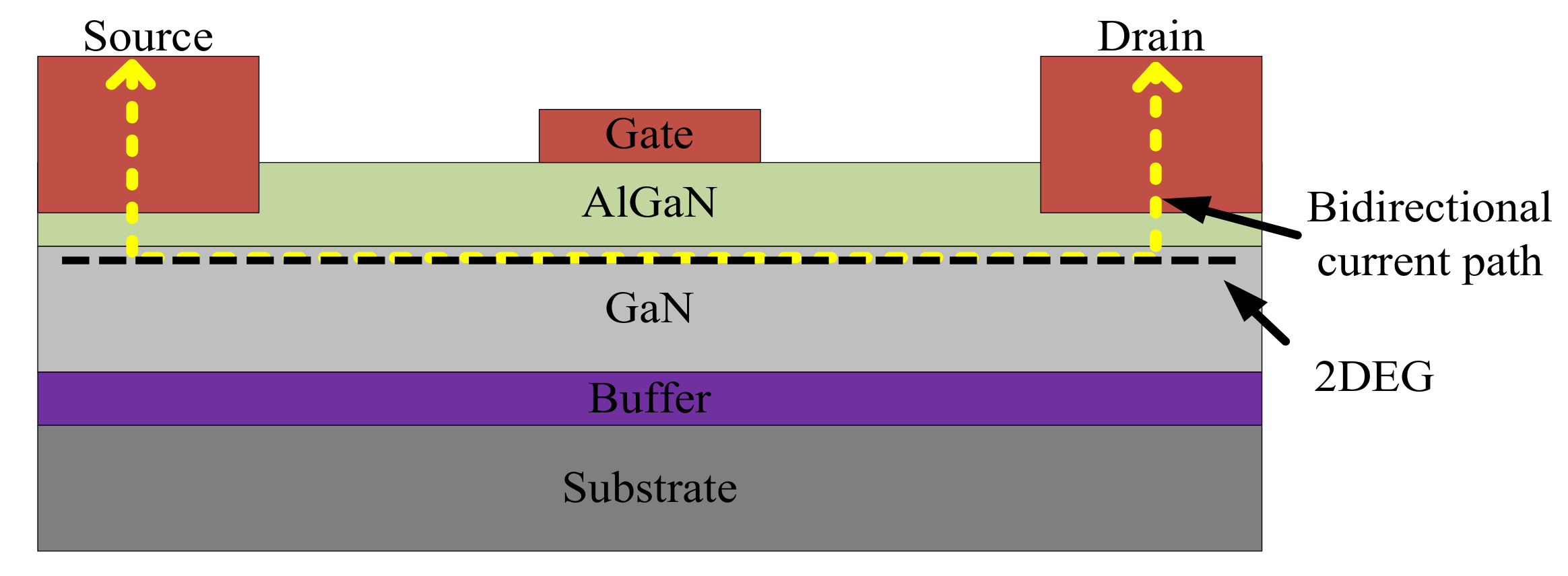
Figure 2.
D-mode GaN high electron mobility transistors (HEMT).
Figure 2.
D-mode GaN high electron mobility transistors (HEMT).
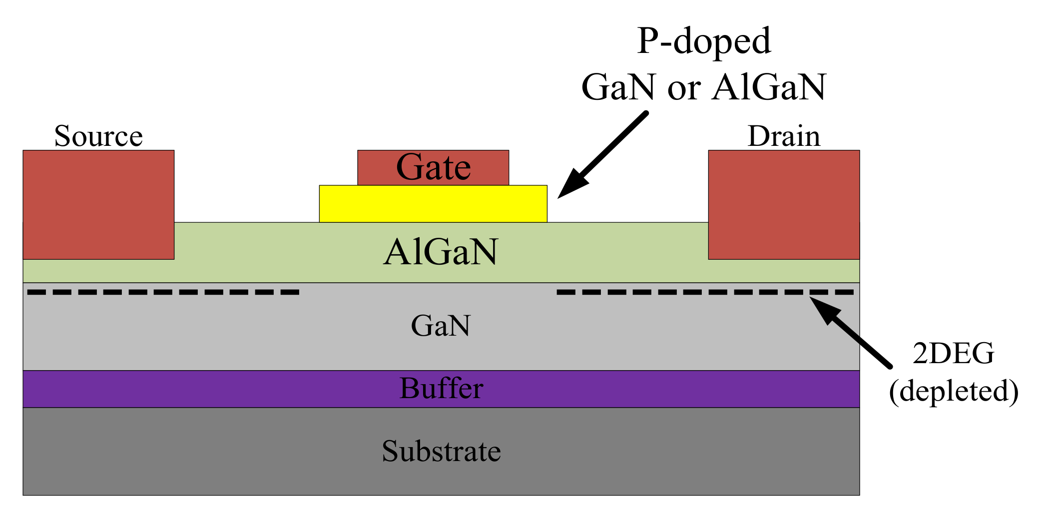
Figure 3.
E-mode GaN HEMT.
Figure 3.
E-mode GaN HEMT.
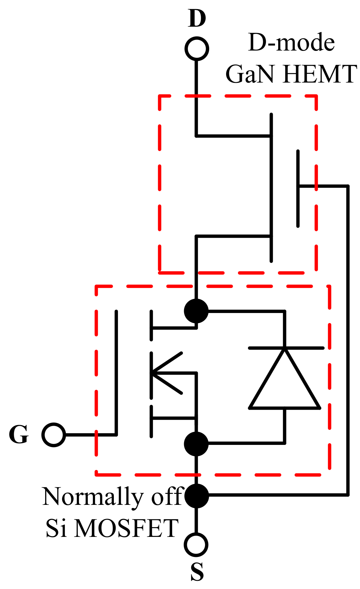
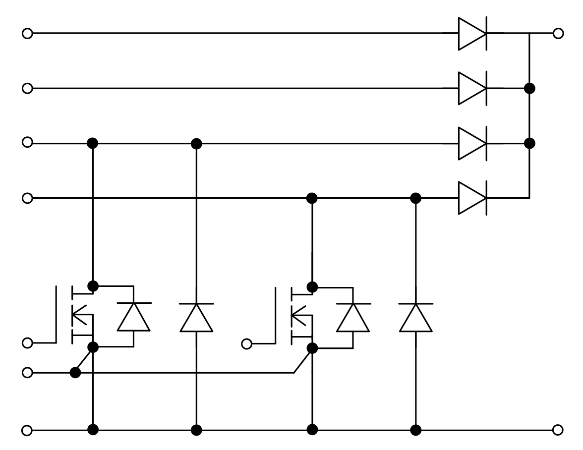
Figure 4.
Cascode GaN HEMT.
Figure 4.
Cascode GaN HEMT.
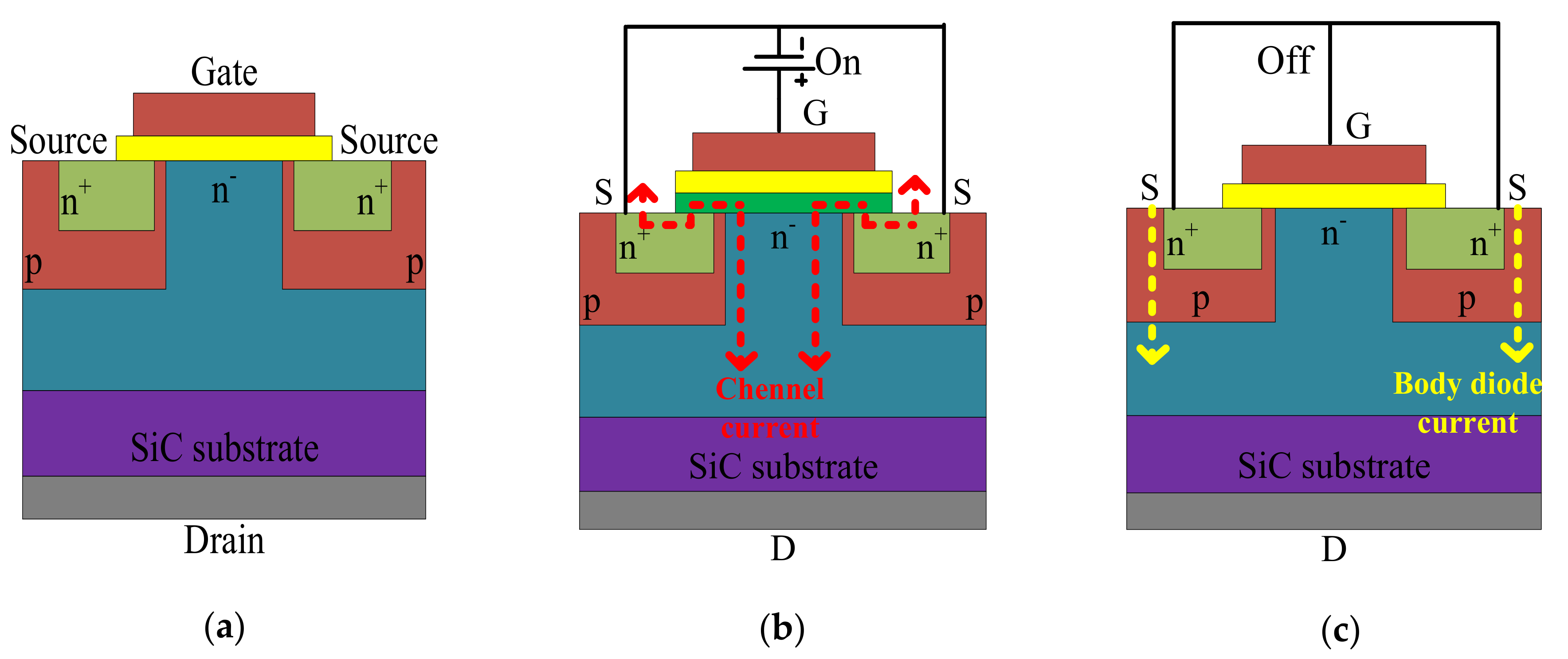
Figure 5.
Schematic diagrams of a SiC MOSFET, (a) basic structure, (b) the gate-source voltage and current path in on-state, (c) the gate-source voltage and current path in off-state.
Figure 5.
Schematic diagrams of a SiC MOSFET, (a) basic structure, (b) the gate-source voltage and current path in on-state, (c) the gate-source voltage and current path in off-state.
Figure 6.
Applications fields of Si, SiC, and GaN switching devices [
13].
Figure 6.
Applications fields of Si, SiC, and GaN switching devices [
13].
Figure 7.
Configurations of Infineon Technologies SiC switching modules DF23MR12W1M1P_B11, DF23MR12W1M1_B11, DF11MR12W1M1P_B11, and DF11MR12W1M1_B11 [
13].
Figure 7.
Configurations of Infineon Technologies SiC switching modules DF23MR12W1M1P_B11, DF23MR12W1M1_B11, DF11MR12W1M1P_B11, and DF11MR12W1M1_B11 [
13].
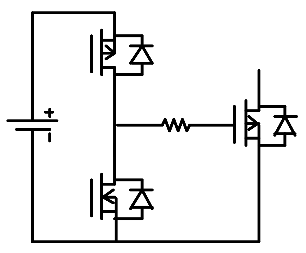
Figure 8.
Conventional totem-pole gate driver.
Figure 8.
Conventional totem-pole gate driver.
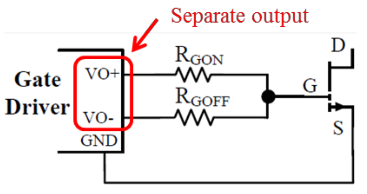
Figure 9.
Gate driver with separate high and low outputs [
31].
Figure 9.
Gate driver with separate high and low outputs [
31].
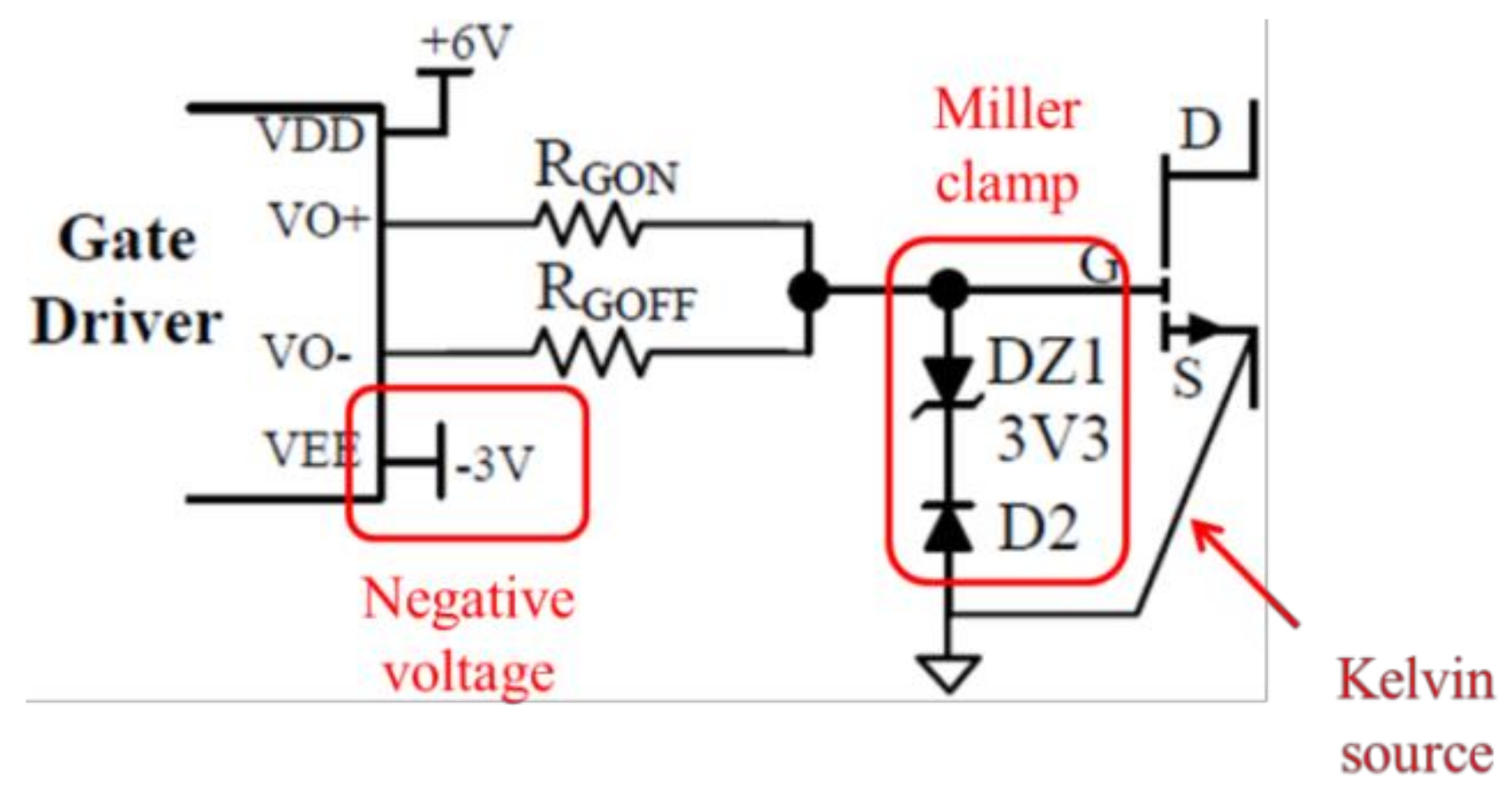
Figure 10.
Driving loop with active Miller clamp, Kelvin source connection, and negative turn-off voltage [
31].
Figure 10.
Driving loop with active Miller clamp, Kelvin source connection, and negative turn-off voltage [
31].
Table 1.
General comparison of normally off GaN high electron mobility transistors (HEMTs).
Table 1.
General comparison of normally off GaN high electron mobility transistors (HEMTs).
| Device | Driving Voltage Threshold | Driving Voltage Range | Operating Temperature | On Resistance | Body Diode |
|---|
| E-mode | <2 V | −10 V~7 V | Higher | Lower | X |
| Cascode | ~4 V | ±20 V | Lower | Higher | O |
Table 2.
General comparison of Si metal-oxide-semiconductor field-effect transistors (MOSFET), normally off GaN HEMTs, and SiC MOSFET.
Table 2.
General comparison of Si metal-oxide-semiconductor field-effect transistors (MOSFET), normally off GaN HEMTs, and SiC MOSFET.
| Device | Driving Voltage Strictness | Power Rating | Switching Speed | On Resistance | Operating Temperature | Body Diode |
|---|
| Si MOSFET | 4th | 2nd | 4th | 4th | 3rd | O |
| E-GaN | Highest | 3rd | Fastest | Lowest | 2nd | X |
| Cascode-GaN | 2nd | 4th | 2nd | 2nd | 3rd | O |
| SiC MOSFET | 3rd | Highest | 3rd | 3rd | Highest | O |
Table 3.
Commercial GaN HEMTs above 600 V.
Table 3.
Commercial GaN HEMTs above 600 V.
| Manufacturer | Type | Vds (V) | Ids (A) | VTH (V) | Vgs (V) | Rds(on) (mΩ) | Ciss (pF) |
|---|
| Infineon Technologies | E-mode | 600 | 10 | 1.2 | −10~5 | 140 | 157 |
| 12.5 |
| 15 | 55 | 380 |
| 31 |
| GaN Systems | 650 | 3.5 | 1.4 | −10~7 | 500 | 30 |
| 7.5 | 1.3 | 200 | 65 |
| 8 | 1.4 | 225 | 52 |
| 11 | 1.5 | 150 | 74 |
| 15 | 1.3 | 100 | 130 |
| 22 | 67 | 195 |
| 30 | 1.7 | 50 | 260 |
| 60 | 1.3 | 25 | 520 |
| 80 | - | - | 18 | - |
| 150 | 10 |
| Panasonic | 600 | 15 | 3.5 | −10~5 | 140 | 160 |
| 31 | 56 | 405 |
| 650 | 9.4 | 270 | 80 |
| Nexperia | Cascode | 650 | 34.5 | 3.9 | ±20 | 50 | 1000 |
| 47.2 | 35 | 1500 |
| Transphorm | 650 | 6.5 | 4 | ±18 | 240 | 760 |
| 15 | ±20 | 150 | 576 |
| 16 | 2.1 | ±18 | 720 |
| 20 | 130 | 760 |
| 25 | 4 | ±20 | 72 | 600 |
| 28 | 2.6 | ±18 | 1130 |
| 34 | 4 | ±20 | 50 | 1000 |
| 60 |
| 36 | 50 |
| 46.5 | 35 | 1500 |
| 47 |
| 900 | 15 | 2.1 | ±18 | 205 | 780 |
| 34 | 3.9 | ±20 | 50 | 980 |
Table 4.
Commercial 600~1200 V SiC MOSFETs by On Semiconductor.
Table 4.
Commercial 600~1200 V SiC MOSFETs by On Semiconductor.
| Vds (V) | Ids (A) | VTH (V) | Vgs (V) | Rds(on) (mΩ) | Ciss (pF) |
|---|
| 900 | 44 | 2.7 | −10~19 | 60 | 1800 |
| 46 | −10~20 | 1770 |
| 112 | 2.6 | −10~19 | 20 | 4415 |
| 118 | 2.7 |
| 1200 | 17 | 3.1 | −15~25 | 160 | 665 |
| 17.3 |
| 19.5 | 3 | 678 |
| 29 | 2.75 | 80 | 1112 |
| 30 | 3 | 1154 |
| 31 | 2.7 | 1112 |
| 58 | 3 | 40 | 1762 |
| 60 | 3 | 1789 |
| 2.97 | 1781 |
| 98 | 2.7 | 20 | 2943 |
| 102 |
| 103 | 2890 |
Table 5.
Commercial 600~1200 V SiC MOSFETs by Littelfuse.
Table 5.
Commercial 600~1200 V SiC MOSFETs by Littelfuse.
| Vds (V) | Ids (A) | VTH (V) | Vgs (V) | Rds(on) (mΩ) | Ciss (pF) |
|---|
| 600 | 15 | 3 | ±20 | 150 | 2000 |
| 1200 | 22 | 2.8 | −10~25 | 160 | 870 |
| 27 | 120 | 1125 |
| 39 | 80 | 1825 |
| 47 | 2.6 | 40 | 1900 |
| 48 | 2.8 | 1895 |
| 68 | 2.6 | 25 | 2790 |
| 90 |
Table 6.
Commercial 600~1200 V SiC MOSFETs by Infineon Technologies.
Table 6.
Commercial 600~1200 V SiC MOSFETs by Infineon Technologies.
| Vds (V) | Ids (A) | VTH (V) | Vgs (V) | Rds(on) (mΩ) | Ciss (pF) |
|---|
| 650 | 20 | 4.5 | −5~23 | 107 | 496 |
| 26 | 72 | 744 |
| 28 |
| 39 | 48 | 1118 |
| 47 | 27 | 2131 |
| 59 |
| 1200 | 4.7 | −7~23 | 350 | 182 |
| 13 | 220 | 289 |
| 19 | 140 | 454 |
| 26 | 90 | 707 |
| 36 | 60 | 1060 |
| 52 | −7~20 | 45 | 2130 |
| −10~20 | 1900 |
| 56 | 4.5 | −7~23 | 30 | 2120 |
Table 7.
Commercial600~1200 V SiC MOSFETs by Cree.
Table 7.
Commercial600~1200 V SiC MOSFETs by Cree.
| Vds (V) | Ids (A) | VTH (V) | Vgs (V) | Rds(on) (mΩ) | Ciss (pF) |
|---|
| 650 | 36 | 2.3 | −8~19 | 60 | 1020 |
| 37 |
| 120 | 15 | 5011 |
| 900 | 11.5 | 2.1 | −8~18 | 280 | 150 |
| 22 | −8~19 | 120 | 350 |
| 23 | −8~18 |
| 35 | −8~19 | 65 | 760 |
| 660 |
| 36 | −8~18 | 760 |
| 63 | 2.4 | −8~19 | 30 | 1747 |
| 1000 | 22 | 2.1 | −8~19 | 120 | 350 |
| 35 | 65 | 660 |
| 1200 | 7.2 | 2.5 | −8~19 | 350 | 345 |
| 7.6 |
| 10 | 2.6 | −10~25 | 280 | 259 |
| 17 | 2.8 | −8~19 | 160 | 632 |
| 18 | 2.9 | −10~25 | 606 |
| 30 | 2.5 | −8~19 | 75 | 1350 |
| 1390 |
| 36 | 2.9 | −10~25 | 80 | 1130 |
| 60 | 2.6 | 40 | 1893 |
| 63 | 2.5 | −8~19 | 32 | 3357 |
| 90 | 2.6 | −10~25 | 25 | 2788 |
| 100 | 2.5 | −8~19 | 21 | 4818 |
| 115 | 16 | 6085 |
Table 8.
Commercial 600~1200 V SiC MOSFETs by Rohm Semiconductor.
Table 8.
Commercial 600~1200 V SiC MOSFETs by Rohm Semiconductor.
| Vds (V) | Ids (A) | VTH (V) | Vgs (V) | Rds(on) (mΩ) | Ciss (pF) |
|---|
| 650 | 21 | 2.7 | −4~26 | 120 | 460 |
| 29 | 2.8 | −10~26 | 120 | 1200 |
| 30 | 2.7 | −4~26 | 80 | 571 |
| 39 | 60 | 852 |
| 70 | 30 | 1526 |
| 93 | 22 | 2208 |
| 118 | 17 | 2884 |
Table 9.
Commercial 600~1200 V SiC MOSFETs by STMicroelectronics.
Table 9.
Commercial 600~1200 V SiC MOSFETs by STMicroelectronics.
| Vds (V) | Ids (A) | VTH (V) | Vgs (V) | Rds(on) (mΩ) | Ciss (pF) |
|---|
| 650 | 45 | 3.2 | −10~22 | 45 | 1370 |
| 55 |
| 75 |
| 90 | 18 | 3300 |
| 95 | 3.1 | 20 | 3315 |
| 100 |
| 116 | 3.2 | 15 | 3380 |
| 119 | 18 |
| 1200 | 12 | 3.5 | −10~25 | 520 | 290 |
| 300 |
| 20 | 189 | 650 |
| 33 | 3.2 | −10~22 | 75 | 1230 |
| 45 | 3.5 | −10~25 | 90 | 1700 |
| 52 | 3.1 | −10~22 | 45 | 2086 |
| 65 | 3 | −10~25 | 59 | 1900 |
| 75 | 3.1 | −10~22 | 30 | 3400 |
| 91 | 3.45 | 21 | 3540 |
Table 10.
Commercial 600~1200 V SiC MOSFETs by United Silicon Carbide.
Table 10.
Commercial 600~1200 V SiC MOSFETs by United Silicon Carbide.
| Vds (V) | Ids (A) | VTH (V) | Vgs (V) | Rds(on) (mΩ) | Ciss (pF) |
|---|
| 650 | 18 | 5 | ±25 | 34 | 1500 |
| 45 |
| 25 | 80 |
| 111 |
| 31 | 80 |
| 41 | 42 |
| 54 |
| 65 | 27 |
| 85 |
| 120 | 4.7 | ±20 | 6.7 | 8360 |
| 1200 | 7.6 | 4.7 | ±25 | 410 | 740 |
| 18.4 | 4.4 | 150 | 738 |
| 33 | 5 | 80 | 1500 |
| 34.5 | 70 |
| 65 | 35 |
| 107 | 4.7 | ±20 | 16 | 7824 |
| 120 | 8.6 | 8512 |
Table 11.
Commercial 600~1200 V SiC MOSFETs by Microchip.
Table 11.
Commercial 600~1200 V SiC MOSFETs by Microchip.
| Vds (V) | Ids (A) | VTH (V) | Vgs (V) | Rds(on) (mΩ) | Ciss (pF) |
|---|
| 700 | 25 | 2.4 | −10~23 | 90 | 785 |
| 28 | 86 |
| 37 | 60 | 1175 |
| 39 |
| 65 | 2.7 | 35 | 2010 |
| 77 |
| 126 | 2.4 | 15 | 4500 |
| 140 | −10~25 |
| 1200 | 35 | 2.8 | −10~23 | 80 | 838 |
| 37 |
| 53 | −10~25 | 40 | 1990 |
| 64 | 2.6 | −10~23 | 40 | 1990 |
| 66 | 2.7 |
| 77 | 2.8 | −10~25 | 25 | 3020 |
| 89 | −10~23 |
| 103 |
Table 12.
Commercial 600~1200 V SiC MOSFETs by GeneSiC.
Table 12.
Commercial 600~1200 V SiC MOSFETs by GeneSiC.
| Vds (V) | Ids (A) | VTH (V) | Vgs (V) | Rds(on) (mΩ) | Ciss (pF) |
|---|
| 1200 | 8 | 3 | −10~25 | 350 | 225 |
| 16 | 160 | 493 |
| 32 | 75 | 1053 |
| 33 |
| 57 | 40 | 1974 |
| 59 |
| 74 | 30 | 2633 |
| 78 |
| 95 | 20 | 3949 |
| 107 |
Table 13.
Commercial GaN HEMT modules by EPC.
Table 13.
Commercial GaN HEMT modules by EPC.
| Configuration | Voltage Rating (V) | Current Rating (A) |
|---|
| HB | 30 | 10/40 |
| 16 |
| 60 | 10/40 |
| 30 |
| 80 | 10/40 |
| 30 |
| 100 | 1.7 |
| 30 |
| HB + bootstrap | 60 | 1.7/0.5 |
| 100 |
| Dual common source | 120 | 3.4 |
Table 14.
Commercial SiC MOSFET modules by Infineon Technologies.
Table 14.
Commercial SiC MOSFET modules by Infineon Technologies.
| Configuration | Voltage Rating (V) | Current Rating (A) |
|---|
| HB | 1200 | 25 |
| 50 |
| 100 |
| 150 |
| 200 |
| 250 |
| 375 |
| 500 |
| FB | 50 |
| HB (3-arm) | 25 |
| Figure 7 | 25 |
| 50 |
Vienna rectifier
phase leg | 75 |
| 100 |
Table 15.
Commercial SiC MOSFET modules by Cree.
Table 15.
Commercial SiC MOSFET modules by Cree.
| Configuration | Voltage Rating (V) | Current Rating (A) |
|---|
| HB | 1200 | 20 |
| 50 |
| 120 |
| 225 |
| 300 |
| 325 |
| 400 |
| 425 |
| 450 |
| Three-phase | 20 |
| 50 |
Table 16.
Commercial SiC MOSFET modules by Rohm Semiconductor.
Table 16.
Commercial SiC MOSFET modules by Rohm Semiconductor.
| Configuration | Voltage Rating (V) | Current Rating (A) |
|---|
| HB | 1200 | 80 |
| 134 |
| 180 |
| 204 |
| 250 |
| 300 |
| 358 |
| 397 |
| 576 |
| Chopper | 134 |
| 180 |
| 204 |
| 300 |
| 358 |
| 576 |
Table 17.
Commercial SiC MOSFET modules by Microchip.
Table 17.
Commercial SiC MOSFET modules by Microchip.
| Configuration | Voltage Rating (V) | Current Rating (A) |
|---|
| HB | 700 | 124 |
| 241 |
| 353 |
| 1200 | 55 |
| 89 |
| 173 |
| 254 |
| 337 |
| 495 |
| 733 |
| 805 |
| 947 |
| 1700 | 50 |
| 100 |
| 280 |
| FB | 700 | 98 |
| 1200 | 55 |
| 89 |
| 173 |
| HB (3-arm) | 700 | 98 |
| 189 |
| 278 |
| 1200 | 89 |
| 171 |
| 251 |
| Chopper | 700 | 98 |
| 1200 | 55 |
| 89 |
| 173 |
| 254 |
| Vienna rectifier phase leg | 700 | 124 |
| 238 |
Table 18.
Commercial SiC MOSFET modules by Powerex.
Table 18.
Commercial SiC MOSFET modules by Powerex.
| Configuration | Voltage Rating (V) | Current Rating (A) |
|---|
| Split dual SiC MOSFET | 1200 | 100 |
| Dual MOSFET | 1700 | 540 |
Table 19.
Commercial SiC MOSFET modules by SemiQ.
Table 19.
Commercial SiC MOSFET modules by SemiQ.
| Configuration | Voltage Rating (V) | Current Rating (A) |
|---|
| HB | 1200 | 160 |
| 200 |
| 240 |
| 320 |
| HB (2-arm) | 40 |
| 80 |
| FB | 20 |
| HB (3-arm) | 20 |
Table 20.
Commercial GaN HEMT drivers by Infineon Technologies.
Table 20.
Commercial GaN HEMT drivers by Infineon Technologies.
| Num. of Channels | Peak Source Current (A) | Peak Sink Current (A) | Supply Voltage (V) | Rise Time (ns) | Fall Time (ns) | Prop. Delay (ns) |
|---|
| 1 | 4 | 8 | 3~20 | 6.5 | 4.5 | 41 |
| 2 | 1 | 2 | 37 |
| 4 | 8 |
Table 21.
Commercial GaN HEMT driver by On Semiconductor.
Table 21.
Commercial GaN HEMT driver by On Semiconductor.
| Num. of Channels | Peak Source Current (A) | Peak Sink Current (A) | Supply Voltage (V) | Rise Time (ns) | Fall Time (ns) | Prop. Delay (ns) |
|---|
| 2 | 1 | 1.3 | 9~17 | 1 | 1 | 25 |
Table 22.
Commercial GaN HEMT drivers by Maxim Integrated.
Table 22.
Commercial GaN HEMT drivers by Maxim Integrated.
| Num. of Channels | Peak Source Current (A) | Peak Sink Current (A) | Supply Voltage (V) | Rise Time (ns) | Fall Time (ns) | Prop. Delay (ns) |
|---|
| 1 | 3 | 7 | 4~14 | 4~37 | 4~18 | 8 |
| 4 | 2.85 | 3~36 | 3.6 | 2.5 | 35 |
| 5.7 | −16~36 | 1.8 | 53 |
Table 23.
Commercial GaN HEMT drivers by pSemi.
Table 23.
Commercial GaN HEMT drivers by pSemi.
| Num. of Channels | Peak Source Current (A) | Peak Sink Current (A) | Supply Voltage (V) | Rise Time (ns) | Fall Time (ns) | Prop. Delay (ns) |
|---|
| 2 | 2 | 4 | 4~6.5 | 1 | 1 | 11 |
| 4~6 | 0.9 | 0.9 | 9.1 |
Table 24.
Commercial GaN HEMT drivers by Silicon Laboratories.
Table 24.
Commercial GaN HEMT drivers by Silicon Laboratories.
| Num. of Channels | Peak Source Current (A) | Peak Sink Current (A) | Supply Voltage (V) | Rise Time (ns) | Fall Time (ns) | Prop. Delay (ns) |
|---|
| 1 | 0.3 | 0.5 | 6.5~24 | 20 | 20 | 60 |
| 1.5 | 2.5 |
| 2.8 | 3.4 | 2.8~30 | 5.5 | 8.5 | 40 |
| 2 | 0.25 | 0.5 | 3~30 | 20 | 20 | 30 |
| 0.4 | 0.6 | 6.5~30 | 5.5 | 8.5 | 40 |
| 1.8 | 4 | 2.5~30 | 10.5 | 13.3 | 45 |
| 2 | 2.5~24 | 12 | 12 | 30 |
| 3~30 |
Table 25.
Commercial GaN HEMT drivers by Texas Instruments.
Table 25.
Commercial GaN HEMT drivers by Texas Instruments.
| Num. of Channels | Peak Source Current (A) | Peak Sink Current (A) | Supply Voltage (V) | Rise Time (ns) | Fall Time (ns) | Prop. Delay (ns) |
|---|
| 1 | 1.3 | 7.6 | 4~12.6 | 12 | 3 | 12 |
| 4 | 4 | 4.5~18 | 9 | 7 | 13 |
| 8 | 7 | 17 |
| 6 | 4~18 | 9 | 4 | 14 |
| 3~18 | 5 | 6 | 27 |
| 8 | 4.5~18 | 9 | 7 | 13 |
| 5 | 5 | 3~33 | 10 | 10 | 65 |
| 7 | 4.75~5.25 | 0.4 | 0.4 | 2.5 |
| 0.65 | 0.85 | 2.9 |
| 2 | 1.2 | 5 | 4.5~5.5 | 7 | 3.5 | 30 |
| 35 |
| 1.5 | 2.5 | 3~18 | 8 | 9 | 28 |
| 3 | 3.8~18 | 0.5 | 0.5 | 10 |
| 4 | 6 | 3~18 | 5 | 6 | 25 |
| 28 |
| 3~25 | 6 | 8 | 19 |
| 7 |
| 5 | 5 | 4.5~18 | 7 | 6 | 13 |
| 9 | 6 | 17 |
Table 26.
Commercial switch-driver-integrated module by EPC.
Table 26.
Commercial switch-driver-integrated module by EPC.
| Configuration | Voltage Rating (V) | Current Rating (A) | Supply Voltage (V) |
|---|
| HB | 70 | 12.5 | 11~13 |
Table 27.
Commercial switch-driver-integrated module by Texas Instruments.
Table 27.
Commercial switch-driver-integrated module by Texas Instruments.
| Configuration | Voltage Rating (V) | Current Rating (A) | Supply Voltage (V) |
|---|
| Single switch | 600 | 17 | 9.5~18 |
| 40 | 9.5~18 |
| 34 | 9.5~18 |
| HB | 80 | 10 | 4.57~5.25 |
Table 28.
Commercial switch-driver-integrated module by Navitas Semiconductor.
Table 28.
Commercial switch-driver-integrated module by Navitas Semiconductor.
| Configuration | Voltage Rating (V) | Current Rating (A) | Supply Voltage (V) |
|---|
| Single switch | 650 | 5 | 5.5~24 |
| 8 |
| 12 |
Table 29.
Commercial SiC MOSFET drivers by Infineon Technologies.
Table 29.
Commercial SiC MOSFET drivers by Infineon Technologies.
| Num. of Channels | Peak Source Current (A) | Peak Sink Current (A) | Supply Voltage (V) | Rise Time (ns) | Fall Time (ns) | Prop. Delay (ns) |
|---|
| 1 | 2 | 2 | −12~28 | 34 | 50 | 170 |
| 4 | 3.5 | 3.1~35 | 10 | 9 | 125 |
| 4.4 | 4.1 | 3.1~18 | 9 | 6 | 300 |
| 10 | 9.4 | 3.1~35 | 10 | 9 | 125 |
| 2 | 2 | 2 | −12~28 | 30 | 50 | 170 |
| 4 | 8 | 3~20 | 6.5 | 4.5 | 37 |
Table 30.
Commercial SiC MOSFET drivers by On Semiconductor.
Table 30.
Commercial SiC MOSFET drivers by On Semiconductor.
| Num. of Channels | Peak Source Current (A) | Peak Sink Current (A) | Supply Voltage (V) | Rise Time (ns) | Fall Time (ns) | Prop. Delay (ns) |
|---|
| 1 | 6 | 6 | −8~22 | 8 | 8 | 25 |
| 7.8 | 7.1 | −10~24 | 10 | 15 | 66 |
| 2 | 1.9 | 2.3 | 0~20 | 13 | 8 | 90 |
Table 31.
Commercial SiC MOSFET drivers by Microchip.
Table 31.
Commercial SiC MOSFET drivers by Microchip.
| Num. of Channels | Peak Source Current (A) | Peak Sink Current (A) | Supply Voltage (V) | Rise Time (ns) | Fall Time (ns) | Prop. Delay (ns) |
|---|
| 2 | 10 | 10 | 14~16 | 80 | 90 | 250 |
| 20 | 20 |
Table 32.
Commercial SiC MOSFET drivers by Maxim Integrated.
Table 32.
Commercial SiC MOSFET drivers by Maxim Integrated.
| Num. of Channels | Peak Source Current (A) | Peak Sink Current (A) | Supply Voltage (V) | Rise Time (ns) | Fall Time (ns) | Prop. Delay (ns) |
|---|
| 1 | 4 | 2.85 | 3~36 | 3.6 | 2.5 | 35 |
| 5.7 | −16~36 | 1.8 | 53 |
Table 33.
Commercial SiC MOSFET drivers by Silicon Laboratories.
Table 33.
Commercial SiC MOSFET drivers by Silicon Laboratories.
| Num. of Channels | Peak Source Current (A) | Peak Sink Current (A) | Supply Voltage (V) | Rise Time (ns) | Fall Time (ns) | Prop. Delay (ns) |
|---|
| 1 | 2.8 | 3.4 | 0~30 | 5.5 | 8.5 | 40 |
| 4 | 4 | 3~30 | 12 | 12 | 19 |
| 2 | 1.8 | 4 | 2.5~30 | 10.5 | 13.3 | 45 |
| 4 | 3~30 | 12 | 12 | 19 |
| 89 |
| 39 |
Table 34.
Commercial SiC MOSFET drivers by Texas Instruments.
Table 34.
Commercial SiC MOSFET drivers by Texas Instruments.
| Num. of Channels | Peak Source Current (A) | Peak Sink Current (A) | Supply Voltage (V) | Rise Time (ns) | Fall Time (ns) | Prop. Delay (ns) |
|---|
| 1 | 1.5 | 2 | −13~33 | 28 | 25 | 70 |
| 2.5 | 5 | −15~30 | 18 | 20 | 76 |
| 0~30 |
| −5~32 | 15 | 7 | 17 |
| 4.5 | 5.3 | −13~33 | 28 | 25 | 70 |
| 8.5 | 10 | −16~33 | 10 | 10 | 65 |
| 10 | −5~15 | 33 | 27 | 90 |
| −5~15 | 28 | 24 | 90 |
| −16~33 | 10 | 10 | 65 |
| 3~33 |
| 15 | 15 | −12~30 | 150 | 150 | 150 |
| 17 | 17 | −16~33 | 10 | 10 | 65 |
| 2 | 4 | 6 | 3~25 | 6 | 7 | 19 |
Table 35.
Commercial SiC MOSFET drivers by Analog Devices.
Table 35.
Commercial SiC MOSFET drivers by Analog Devices.
| Num. of Channels | Peak Source Current (A) | Peak Sink Current (A) | Supply Voltage (V) | Rise Time (ns) | Fall Time (ns) | Prop. Delay (ns) |
|---|
| 1 | 0.2 | 0.2 | 4.5~17 | 15 | 15 | 60 |
| 2 | 2 | 2.5~35 | 18 | 18 | 38 |
| 3.3~35 | 17 | 17 | 30 |
| 2.3 | 2.3 | 2.5~35 | 18 | 18 | 43 |
| 4 | 4 | 3~18 | 12 | 12 | 46 |
| 22 | 22 | 53 |
| −15~30 | 16 | 16 | 55 |
| −15~35 |
| 6 | 6 | 4.5~25 | - | - | 107 |
| 6~25 | - | - | 100 |
| 2 | 0.1 | 0.1 | 4.5~18 | 25 | 25 | 124 |
| 0.3 | 4.5~18.5 | 10 | 100 |
| 4 | 4 | 3~18 | 12 | 12 | 47 |
| 46 |
| 4.5~18 | 14 | 14 | 160 |
Table 36.
Commercial SiC MOSFET drivers by Tamura.
Table 36.
Commercial SiC MOSFET drivers by Tamura.
| Num. of Channels | Peak Source Current (A) | Peak Sink Current (A) | Supply Voltage (V) | Rise Time (ns) | Fall Time (ns) | Prop. Delay (ns) |
|---|
| 2 | 1.8 | 1.8 | 13.5~26.4 | - | - | 90 |
| 2.5 | 3.5 | - | - |
| 3 | 3 | | |
| 4 | 4 | - | - |
| 4.5 | 4.5 | - | - |
| 6 | 6 | - | - |
| 7 | 7 | - | - |
| 18 | 18 | - | - | 80 |
| 43 | 43 | - | - | 100 |
Table 37.
Commercial SiC MOSFET drivers by Rohm Semiconductor, Littelfuse, Diodes Incorporated, NXP Semiconductors, and Power Integrations.
Table 37.
Commercial SiC MOSFET drivers by Rohm Semiconductor, Littelfuse, Diodes Incorporated, NXP Semiconductors, and Power Integrations.
| MFR | Num. of Channels | Peak Source Current (A) | Peak Sink Current (A) | Supply Voltage (V) | Rise Time (ns) | Fall Time (ns) | Prop. Delay (ns) |
|---|
| Rohm | 1 | >4 (self-limited) | >4 (self-limited) | 4.5~20 | 15 | 15 | 65 |
| Littelfuse | 9 | 9 | −10~25 | 10 | 10 | 75 |
| Diodes | 10 | 10 | 40 | 48 | 35 | 10 |
| NXP | 15 | 15 | −12~40 | - | - | - |
| Power Int. | 8 | 8 | 4.75~28 | 113 | 105 | 270 |
Table 38.
Reviewed GaN HEMT driving circuits.
Table 38.
Reviewed GaN HEMT driving circuits.
| Ref | Channel per Driver | fsw (kHz) | System Pout | System Efficiency | GaN HEMT | Commercial Driver |
|---|
| [46] | 1 | 160 | 2.5 kW | 97.3% | PGA26A10DS | ACPL-P346 |
| [47] | 10 | 1 kW | unrevealed | GS66508T | UCC27511 |
| [48] | 100 | 1.5 kW | >97% | GS66508T | Si8271 |
| [49] | 120~200 | 3 kW | >99% | GS66508T | N/A |
| [50] | 200 | N/A | N/A | PGA26E19BA |
| [51] | 2 | 100 | 2 kVA | 97.4% | GS66508T | ADuM7223 |
| [52] | 100~250 | 2 kW | 95% | unrevealed | ADuM3223 |
| [53] | 160 | 500 W | 96.2% | GS66502B | Si8274 |
| [54] | - | 800 W | 98% | GS66508B | Si8273 |
| [55] | 65~100 | 1.5 kW | 90% | GS66504B | Si8273 |
| [56] | 25 | unrevealed | unrevealed | GS66508T | N/A |
Table 39.
Reviewed SiC MOSFET driving circuits.
Table 39.
Reviewed SiC MOSFET driving circuits.
| Ref | Channel per Driver | fsw | System Pout | System Efficiency | SiC MOSFET | Commercial Driver |
|---|
| [60] | 1 | N/A | unrevealed | N/A | C2M0025120D | IXDD609SI |
| [61] | 1 MHz | 51 kW | unrevealed | C2M0040120D | ADuM4135 |
| [62] | 4 MHz | 10 kW | >97.5% | C2M0080120D | IXRFD630 |
| [34] | 20 kHz | 5.9 kW | unrevealed | C2M0080120D | N/A |
| [63] | 2 MHz | 600 W | unrevealed | C2M0080120D |
| [64] | 150 kHz | 4 kW | >99% | MT5F31003 |
| [65] | 10 kHz | 30 kW | 99% | CAS300M12BM2 |
| [66] | 100 kHz | 2 kW | 82% | SCH2080KE |
| [67] | unrevealed | 4.5 kW | unrevealed | C2M0025120D |
| [68] | unrevealed | 9 kW | unrevealed | SCH2080KE |
| [69] | 2 | 200 kHz | 1 kW | 96% | SCTMU001F | UCC27531 |
| [70] | 25 kHz | 2.5 kW | N/A | C2M0160120D | ACPL-344JT |
| [71] | 100 kHz | 252 kW | 99.4% | CAS300M17BM2 | STGAP1AS |
| [72] | 100 kHz | 1.8 kW | unrevealed | C2M1000170D | unrevealed |
| [73] | 10 kHz | unrevealed | unrevealed | unrevealed | N/A |


