A Novel Germanium-Around-Source Gate-All-Around Tunnelling Field-Effect Transistor for Low-Power Applications


Abstract
1. Introduction
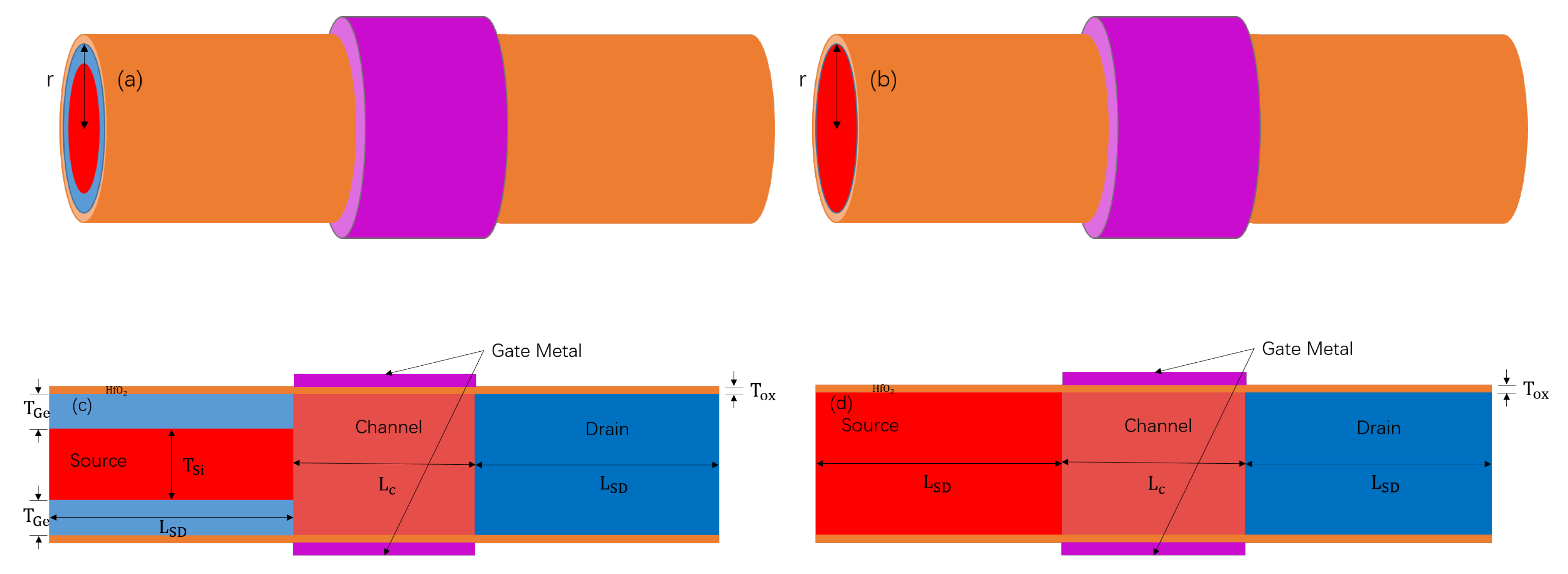
2. Device Structures and Simulation Methods
3. Simulation Results and Discussion
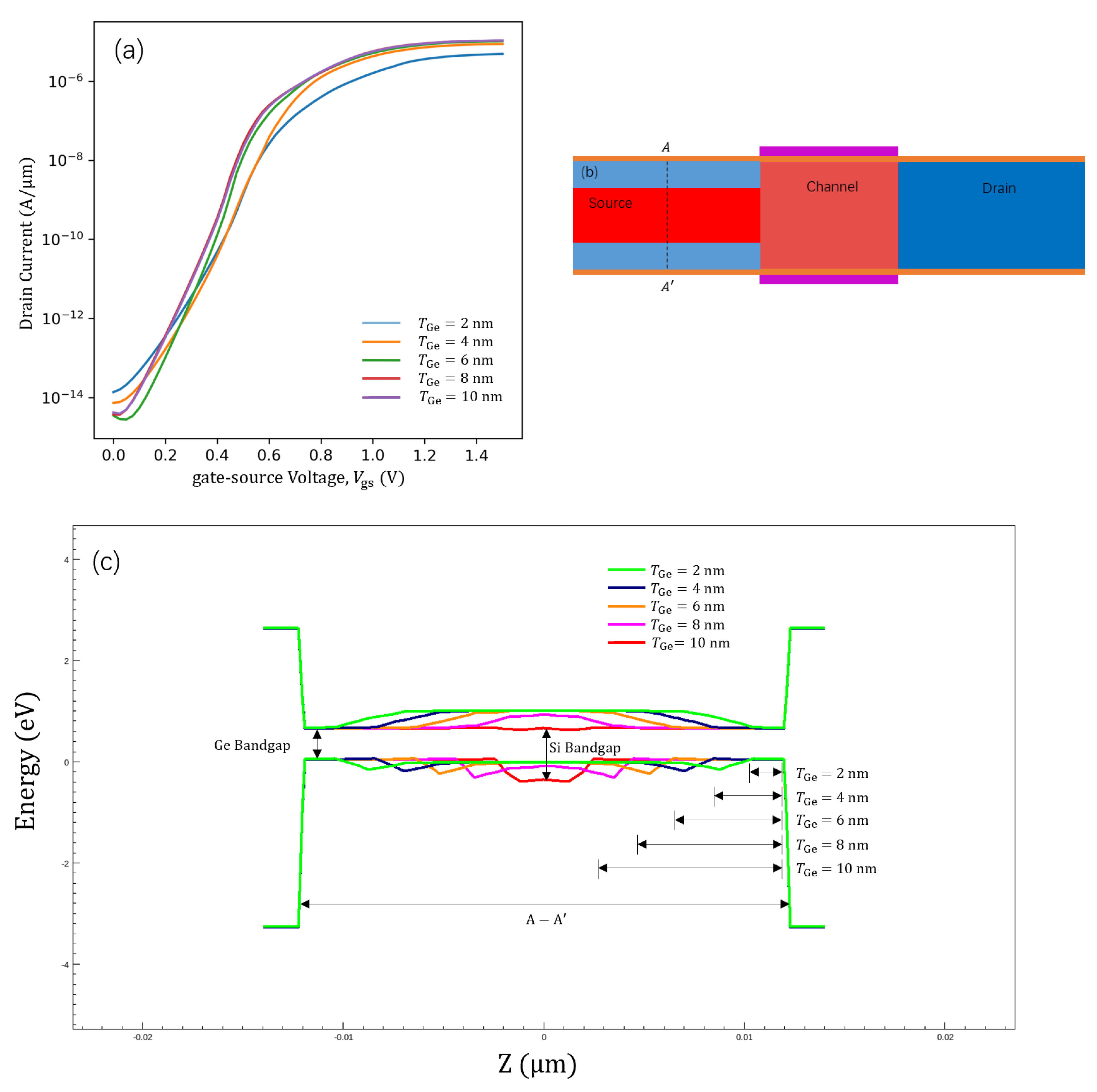
3.1. Thickness of Germanium ()
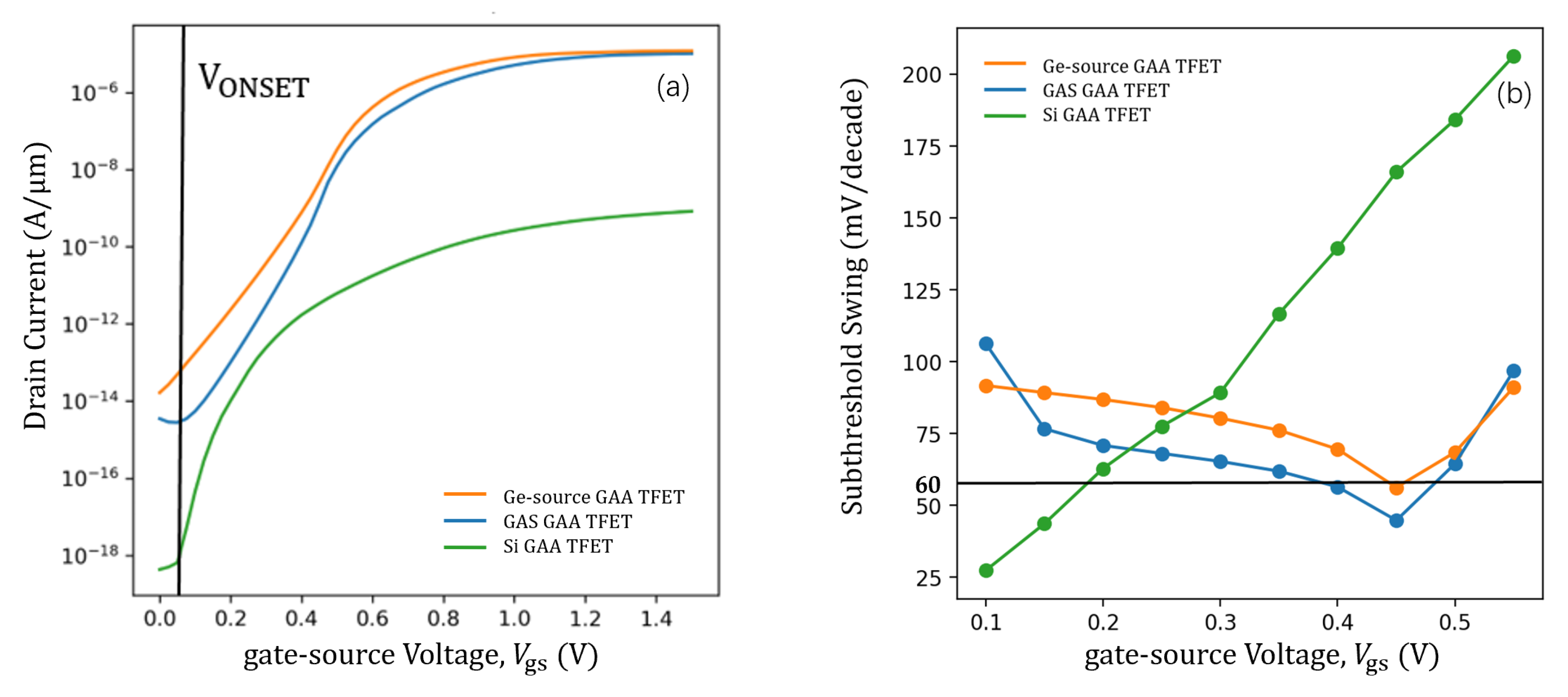
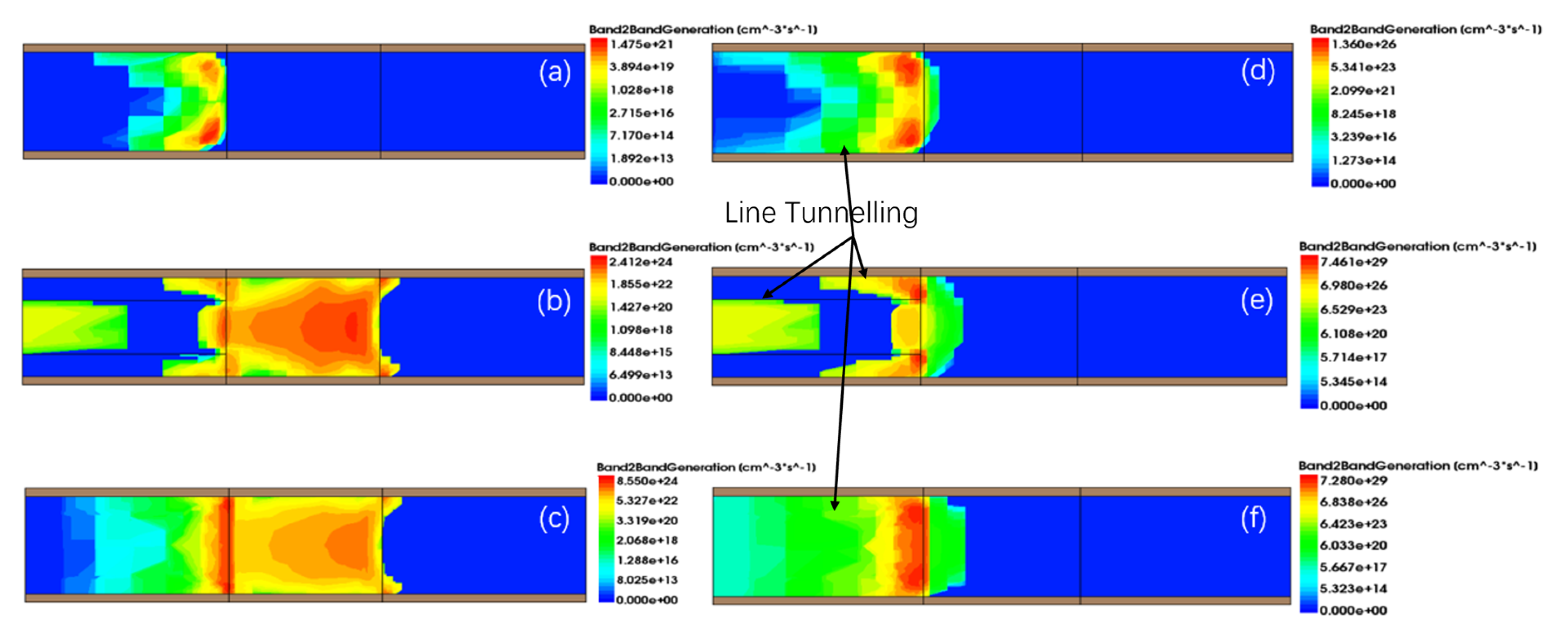
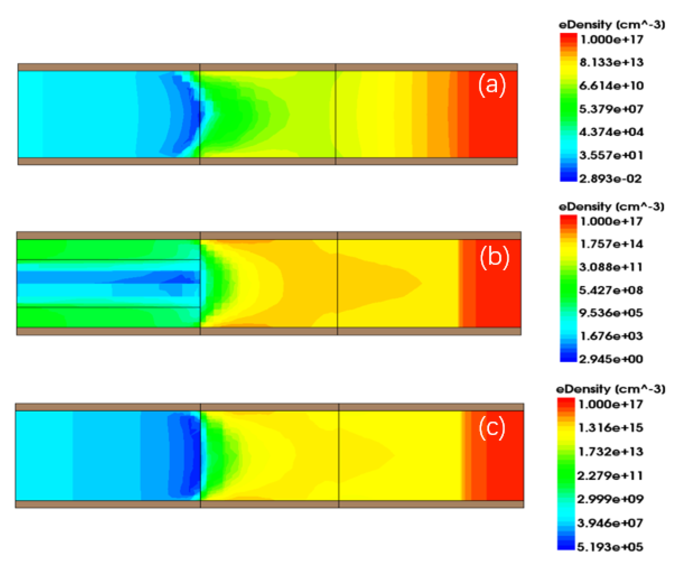
3.2. Effect of Germanium-Around-Source (GAS)
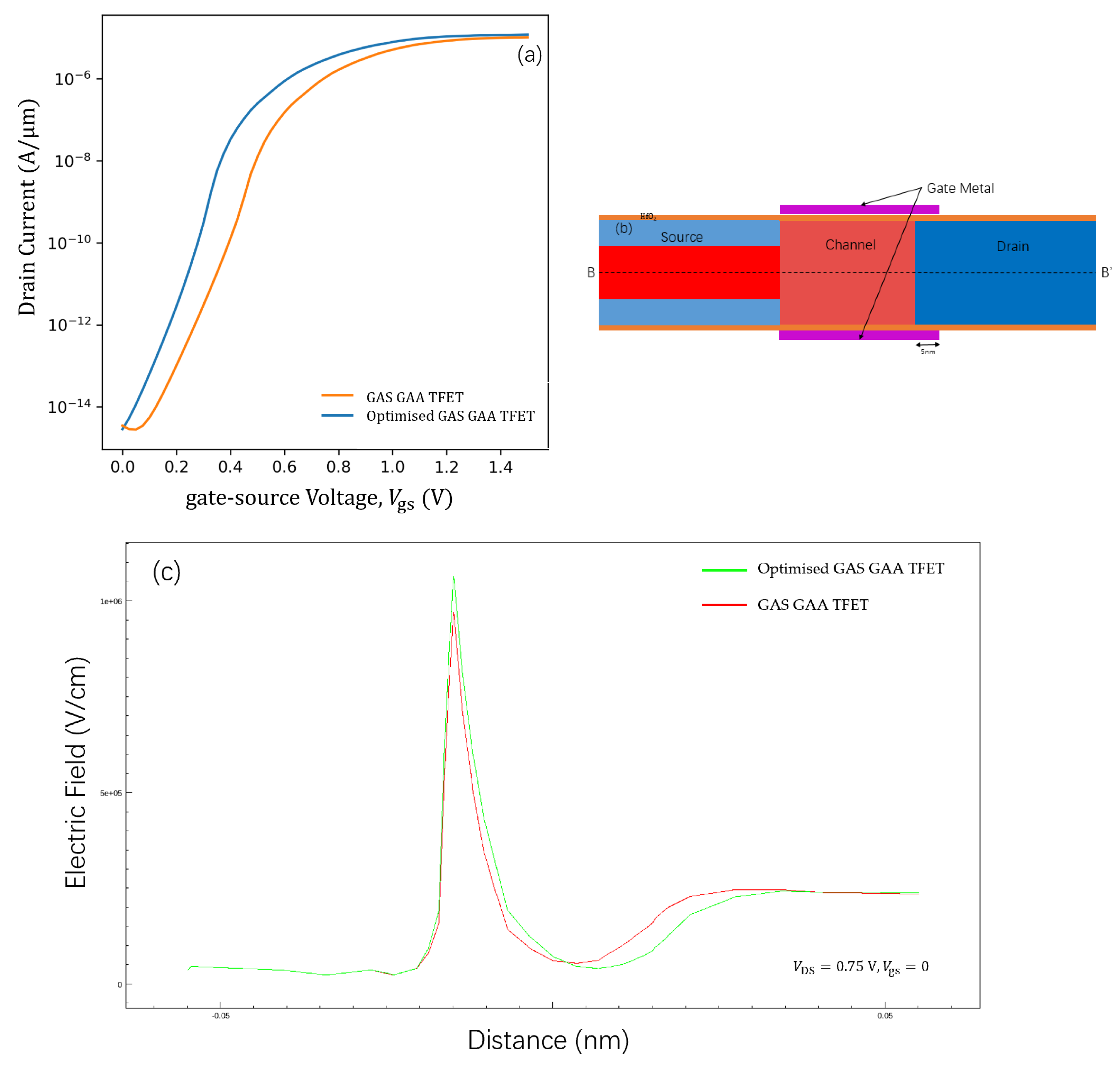
3.3. Optimised GAS GAA TFET
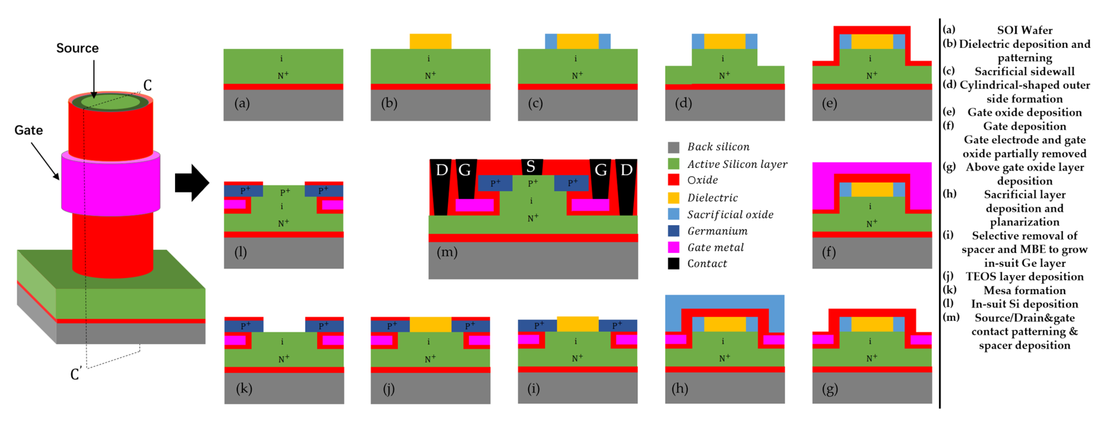
3.4. Process Flow
4. Conclusions
Author Contributions
Funding
Conflicts of Interest
Abbreviations
| BTBT | band-to-band tunnelling |
| band-to-band tunnelling probability | |
| the bandgap of main semiconductor material in device | |
| GAS GAA TFET | germanium-around-source gate-all-around tunnel field-effect transistor |
| Si GAA TFET | silicon gate-all-around tunnel field-effect transistor |
| Ge-source GAA TFET | germanium-based-source gate-all-around tunnel field-effect transistor |
| SS | subthreshold swing |
| minimum point subthreshold swing | |
| average subthreshold swing | |
| ON-state current | |
| OFF-state current | |
| drain current | |
| current at | |
| the voltage where OFF-state current increased by a factor of times | |
| the voltage after which the drain current increases exponentially with the gate voltage | |
| drain-source voltage | |
| gate-source voltage | |
| threshold voltage | |
| EBL | electron beam lithography |
| MBE | molecular beam epitaxy |
| TEOS | Tetraethylortho Silicate |
References
- Musalgaonkar, G.; Sahay, S.; Saxena, R.S.; Kumar, M.J. Nanotube tunnelling FET with a Core Source for Ultrasteep Subthreshold Swing: A Simulation Study. IEEE Trans. Electron Devices 2019, 66, 4425–4432. [Google Scholar] [CrossRef]
- Beohar, A.; Vishvakarma, S.K. Performance enhancement of asymmetrical underlap 3D-cylindrical GAA-TFET with low spacer width. Micro Nano Lett. 2016, 11, 443–445. [Google Scholar] [CrossRef]
- Wu, C.; Huang, Q.; Zhao, Y.; Wang, J.; Wang, Y.; Huang, R. A Novel Tunnel FET Design With Stacked Source Configuration for Average Subthreshold Swing Reduction. IEEE Trans. Electron Devices 2016, 63, 5072–5076. [Google Scholar] [CrossRef]
- Lin, H.H.; Hu, V.P. Device design of vertical nanowire III-V heterojunction TFETs for performance enhancement. In Proceedings of the 2018 7th International Symposium on Next Generation Electronics (ISNE), Taipei, Taiwan, 7–9 May 2018; pp. 1–4. [Google Scholar]
- Seo, J.H.; Yoon, Y.J.; Lee, H.G.; Kang, I.M. Design optimization InGaAs/GaAsSb-based heterojunction Gate-all-around (GAA) arch-shaped tunnelling field-effect transistor (A-TFET). In Proceedings of the 2018 International Conference on Electronics, Information, and Communication (ICEIC), Honolulu, HI, USA, 24–27 January 2018; pp. 1–2. [Google Scholar]
- Gopalakrishnan, K.; Griffin, P.B.; Plummer, J.D. Impact ionization MOS (I-MOS)—Part I: Device and circuit simulations. IEEE Trans. Electron Devices 2005, 52, 69–76. [Google Scholar] [CrossRef]
- Musalgaonkar, G.; Sahay, S.; Saxena, R.S.; Kumar, M.J. An impact ionization MOSFET with reduced breakdown voltage based on backgate misalignment. IEEE Trans. Electron Devices 2018, 66, 868–875. [Google Scholar] [CrossRef]
- Onal, C.; Woo, R.; Koh, H.Y.; Griffin, P.B.; Plummer, J.D. A novel depletion-IMOS (DIMOS) device with improved reliability and reduced operating voltage. IEEE Electron Device Lett. 2009, 30, 64–67. [Google Scholar] [CrossRef]
- Kumar, M.J.; Maheedhar, M.; Varma, P.P. Bipolar I-MOS—An impact-ionization MOS with reduced operating voltage using the openbase BJT configuration. IEEE Trans. Electron Devices 2015, 62, 4345–4348. [Google Scholar] [CrossRef]
- Mamidala, J.K.; Vishnoi, R.; Pandey, P. Tunnel Field-Effect Transistors (TFET); John Wiley and Sons Ltd.: West Sussex, UK, 2016. [Google Scholar]
- Saurabh, S.; Kumar, M.J. Fundamentals of Tunnel Field-Effect Transistors; CRC Press: Boca Raton, FL, USA, 2016. [Google Scholar]
- Abdi, D.B.; Kumar, M.J. In-built N+ pocket p-n-p-n tunnel field-effect transistor. IEEE Electron Device Lett. 2014, 35, 1170–1172. [Google Scholar] [CrossRef]
- Lin, J.T.; Wang, T.C.; Lee, W.H.; Yeh, C.T.; Glass, S.; Zhao, Q.T. Characteristics of recessed-gate TFETs with line tunnelling. IEEE Trans. Electron Devices 2018, 65, 769–775. [Google Scholar] [CrossRef]
- Nagavarapu, V.; Jhaveri, R.; Woo, J.C. The tunnel source (PNPN) n-MOSFET: A novel high performance transistor. IEEE Trans. Electron Devices 2008, 55, 1013–1019. [Google Scholar] [CrossRef]
- Zhu, J.; Zhao, Y.; Huang, Q.; Chen, C.; Wu, C.; Jia, R.; Huang, R. Design and simulation of a novel graded-channel heterojunction tunnel FET with high ION/IOFF ratio and steep swing. IEEE Electron Device Lett. 2017, 38, 1200–1203. [Google Scholar] [CrossRef]
- Beohar, A.; Yadav, N.; Vishvakarma, S.K. Analysis of trap-assisted tunnelling in asymmetrical underlap 3D-cylindrical GAA-TFET based on hetero-spacer engineering for improved device reliability. Micro Nano Lett. 2017, 12, 982–986. [Google Scholar] [CrossRef]
- Musalgaonkar, G.; Sahay, S.; Saxena, R.S.; Kumar, M.J. A Line tunnelling Field-Effect Transistor Based on Misaligned Core–Shell Gate Architecture in Emerging Nanotube FETs. IEEE Trans. Electron Devices 2019, 66, 2809–2816. [Google Scholar] [CrossRef]
- Shirazi, S.G.; Karimi, G.R.; Mirzakuchaki, S. GAA CNT TFETs Structural Engineering: A Higher ON Current, Lower Ambipolarity. IEEE Trans. Electron Devices 2019, 66, 2822–2830. [Google Scholar] [CrossRef]
- Lu, H.; Seabaugh, A. Tunnel field-effect transistors: State-ofthe-art. IEEE J. Electron Devices Soc. 2014, 2, 44–49. [Google Scholar] [CrossRef]
- Huang, Q.; Huang, R.; Wu, C.; Zhu, H.; Chen, C.; Wang, J.; Guo, L.; Wang, R.; Ye, L.; Wang, Y. Comprehensive performance re-assessment of TFETs with a novel design by gate and source engineering from device/circuit perspective. In Proceedings of the 2014 IEEE International Electron Devices Meeting, San Francisco, CA, USA, 15–17 December 2014; pp. 13–33. [Google Scholar]
- Appenzeller, J.; Lin, Y.M.; Knoch, J.; Chen, Z.; Avouris, P. Comparing carbon nanotube transistors-the ideal choice: A novel tunnelling device design. IEEE Trans. Electron Devices 2005, 52, 2568–2576. [Google Scholar] [CrossRef]
- Toh, E.H.; Wang, G.H.; Samudra, G.; Yeo, Y.C. Device physics and design of double-gate tunnelling field-effect transistor by silicon film thickness optimization. Appl. Phys. Lett. 2007, 90, 63507. [Google Scholar] [CrossRef]
- Avci, U.E.; Morris, D.H.; Young, I.A. Tunnel field-effect transistors: Prospects and challenges. IEEE J. Electron Devices Soc. 2015, 3, 88–95. [Google Scholar] [CrossRef]
- Vanlalawpuia, K.; Bhowmick, B. Investigation of a Ge-Source Vertical TFET with Delta-Doped Layer. IEEE Trans. Electron Devices 2019, 66, 4439–4445. [Google Scholar] [CrossRef]
- Kim, S.H.; Jacobson, Z.A.; Liu, T.J. Impact of body doping and thickness on the performance of Germanium-source TFETs. IEEE Trans. Electron Devices 2010, 57, 1710–1713. [Google Scholar] [CrossRef]
- Damrongplasit, N.; Shin, C.; Kim, S.H.; Vega, R.A.; Liu, T.-J.K. Study of Random Dopant Fluctuation Effects in Germanium-Source Tunnel FETs. IEEE Trans. Electron Devices 2011, 58, 3541–3548. [Google Scholar] [CrossRef]
- Lee, Y.; Nam, H.; Park, J.-D.; Shin, C. Study of work-function variation for high-K/metal-gate ge-source tunnel field-effect transistors. IEEE Trans. Electron Devices 2015, 62, 2143–2147. [Google Scholar] [CrossRef]
- Beohar, A.; Shah, A.P.; Yadav, N.; Vishvakarma, S.K. Design of 3D cylindrical GAA-TFET based on germanium source with drain underlap for low power applications. In Proceedings of the 2017 International Conference on Electron Devices and Solid-State Circuits (EDSSC), Hsinchu, Taiwan, 18–20 October 2017; pp. 1–2. [Google Scholar]
- Jhan, Y.-R.; Wu, Y.-C.; Hung, M.-F. Performance enhancement of nanowire tunnel field-effect transistor with asymmetry-gate based on different screening length. IEEE Electron Device Lett. 2013, 34, 1482–1484. [Google Scholar] [CrossRef]
- Kumar, M.J.; Janardhanan, S. Doping-less tunnel field effecttransistor: Design and investigation. IEEE Trans. Electron Devices 2013, 60, 3285–3290. [Google Scholar] [CrossRef]
- Jang, W.D.; Yoon, Y.J.; Cho, M.S.; Jung, J.H.; Lee, S.H.; Jang, J.; Bae, J.-H.; Kang, I.M. Design and Optimization of Germanium-Based Gate-Metal-Core Vertical Nanowire Tunnel FET. Micromachines 2019, 10, 749. [Google Scholar] [CrossRef] [PubMed]
- Raad, B.; Kondekar, P.; Sharma, D.; Nigam, K. Dielectric and work function engineered TFET for ambipolar suppression and RF performance enhancement. Electron. Lett. 2016, 52, 770–772. [Google Scholar] [CrossRef]
- Singh, P.; Chauhan, V.K.; Ray, D.D.; Dash, S.; Mishra, G.P. Ambipolar Performance Improvement of Dual Material TFET Using Drain Underlap Engineering. In Proceedings of the 2018 IEEE Electron Devices Kolkata Conference (EDKCON), Kolkata, India, 24–25 November 2018; pp. 274–277. [Google Scholar]
- Lee, J.S.; Seo, J.H.; Cho, S.; Lee, J.-H.; Kang, S.-W.; Bae, J.-H.; Cho, E.-S.; Kang, I.M. Simulation study on effect of drain underlap in gate-all-around tunnelling field-effect transistors. Curr. Appl. Phys. 2013, 13, 1143–1149. [Google Scholar] [CrossRef]
- Tekleab, D.; Tran, H.H.; Sleight, J.W.; Chidambarrao, D. Silicon Nanotube MOSFET. U.S. Patent 8,871,576, 28 October 2014. [Google Scholar]
- Bae, T.-E.; Suzuki, R.; Nakane, R.; Takenaka, M.; Takagi, S. Effects of ge-source impurity concentration on electrical characteristics of Ge/Si hetero-junction tunnelling FETs. In Proceedings of the 2017 Fifth Berkeley Symposium on Energy Efficient Electronic Systems and Steep Transistors Workshop (E3S), Berkeley, CA, USA, 19–20 October 2017; pp. 1–3. [Google Scholar]


| Parameters | Definations | Value |
|---|---|---|
| r | Device radius | 12 nm |
| Lateral length of source and drain | 40 nm | |
| Lateral length of channel | 30 nm | |
| Gate oxide thickness | 2 nm | |
| Thickness of around-source germanium | Variable | |
| Thickness of silicon surrounded by germanium | Variable | |
| P-type source doping concentration | cm | |
| P-type channel doping concentration | cm | |
| P-type around-source germanium doping concentration | cm | |
| N-type drain doping concentration | cm |
| Si GAA TFET | Ge-Source GAA TFET | GAS GAA TFET | Optimised GAS GAA TFET | |
|---|---|---|---|---|
| (mV/dec.) | 26.835 | 58.645 | 45.720 | 39.501 |
| (mV/dec.) | 68.71 | 83.71 | 65 | 57.29 |
| (A/um) | 11.7 | 10.2 | 11.9 | |
| (A/um) |
© 2020 by the authors. Licensee MDPI, Basel, Switzerland. This article is an open access article distributed under the terms and conditions of the Creative Commons Attribution (CC BY) license (http://creativecommons.org/licenses/by/4.0/).
Share and Cite
Han, K.; Long, S.; Deng, Z.; Zhang, Y.; Li, J. A Novel Germanium-Around-Source Gate-All-Around Tunnelling Field-Effect Transistor for Low-Power Applications. Micromachines 2020, 11, 164. https://doi.org/10.3390/mi11020164
Han K, Long S, Deng Z, Zhang Y, Li J. A Novel Germanium-Around-Source Gate-All-Around Tunnelling Field-Effect Transistor for Low-Power Applications. Micromachines. 2020; 11(2):164. https://doi.org/10.3390/mi11020164
Chicago/Turabian StyleHan, Ke, Shanglin Long, Zhongliang Deng, Yannan Zhang, and Jiawei Li. 2020. "A Novel Germanium-Around-Source Gate-All-Around Tunnelling Field-Effect Transistor for Low-Power Applications" Micromachines 11, no. 2: 164. https://doi.org/10.3390/mi11020164
APA StyleHan, K., Long, S., Deng, Z., Zhang, Y., & Li, J. (2020). A Novel Germanium-Around-Source Gate-All-Around Tunnelling Field-Effect Transistor for Low-Power Applications. Micromachines, 11(2), 164. https://doi.org/10.3390/mi11020164