Article

Investigation of Recessed Gate AlGaN/GaN MIS-HEMTs with Double AlGaN Barrier Designs toward an Enhancement-Mode Characteristic

International College of Semiconductor Technology, National Chiao Tung University, Hsinchu 30010, Taiwan
*
Author to whom correspondence should be addressed.
Micromachines 2020, 11(2), 163; https://doi.org/10.3390/mi11020163
Submission received: 31 December 2019 / Revised: 1 February 2020 / Accepted: 2 February 2020 / Published: 3 February 2020
(This article belongs to the Special Issue Wide Bandgap Based Devices: Design, Fabrication and Applications)

Abstract

:
In this work, recessed gate AlGaN/GaN metal-insulator-semiconductor high-electron-mobility transistors (MIS-HEMTs) with double AlGaN barrier designs are fabricated and investigated. Two different recessed depths are designed, leading to a 5 nm and a 3 nm remaining bottom AlGaN barrier under the gate region, and two different Al% (15% and 20%) in the bottom AlGaN barriers are designed. First of all, a double hump trans-conductance (gm)–gate voltage (VG) characteristic is observed in a recessed gate AlGaN/GaN MIS-HEMT with a 5 nm remaining bottom Al0.2Ga0.8N barrier under the gate region. Secondly, a physical model is proposed to explain this double channel characteristic by means of a formation of a top channel below the gate dielectric under a positive VG. Finally, the impacts of Al% content (15% and 20%) in the bottom AlGaN barrier and 5 nm/3 nm remaining bottom AlGaN barriers under the gate region are studied in detail, indicating that lowering Al% content in the bottom can increase the threshold voltage (VTH) toward an enhancement-mode characteristic.

1. Introduction

AlGaN/GaN high-electron-mobility transistors (HEMTs) are promising for power switching applications due to the wide band gap, large breakdown electric field, and the inherent high electron mobility due to two-dimensional electron gas (2DEG) [1,2]. Normally, conventional AlGaN/GaN Schottky HEMTs suffer high gate leakage, resulting in an unfavorable power loss during an off-state condition and a low gate overdrive during an on-state condition. In order to tackle this issue, Metal-insulator-semiconductors high electrons mobility transistors (MIS-HEMTs) have gained attentions recently [2,3,4]. Inserting a dielectric in the interface between AlGaN and gate metal significantly reduces the gate leakage current, allowing a high gate overdrive to have a fast switch from off-state to on-state operation. Due to a piezoelectric and polarization effects, a two dimensional electron gas (2DEG) is naturally formed in the interface between GaN and AlGaN, leading to depletion mode (VTH<0) characteristics. However, an enhancement mode characteristic is more favorable in practical applications due to a lower power consumption, less failure issues, and a flexible integration. So far, there are several approaches to realize an enhancement mode operation, such as a recessed gate structure [5,6,7], p-GaN/p-AlGaN gate [2,8], Fluoride-based plasma treatment [9], the metal–oxide–semiconductor field-effect transistor structure [10], cascode-based topology in connecting high voltage D-mode HEMTs with a low voltage Si MOSFETs or E-mode HEMTs [11,12], etc. HEMTs with a p-GaN/p-AlGaN gate generally suffer the challenges to effectively dope the Mg into top GaN or AlGaN layer and to remove the top p-GaN/p-AlGaN layer in the access region. The thermal stability of the charges induced by Fluoride-based plasma remains a challenge. The MOS-type GaN FETs suffer the low electron mobility due to the disappearance of the 2DEG. The cascode-based topology with dual GaN-based transistors increase the active area and complicates the layout designs. Therefore, the recessed gate-based HEMT is one of the most popular architectures to obtaining an enhancement-mode characteristic because the 2DEG can be reduced under the gate by using a simple etching process, i.e., Reactive-ion etching (RIE)-based etching or atomic layer etching (ALE). Recently, the recessed gate AlGaN/GaN-based devices show a promising performance toward an enhancement-mode characteristic [5,6,7].
Typically, AlGaN/GaN-based HEMTs are fabricated with the single AlGaN barrier layer. A multi barrier device was demonstrated first in GaAs-based devices in 1985 [13]. Since 1999, a depletion mode double AlGaN barrier design was first demonstrated by Gaska et al. [14]. Afterwards, depletion-mode double AlGaN barrier HEMTs have been explored in details in [15,16,17,18], showing a high current drive due to a second transconductance (gm) and lower access resistance. Furthermore, the recent demonstration using AlGaN/AlN/GaN/AlN epitaxy stack to achieve the double channel has attracted a lot of attentions [19]. Although the demonstration of the GaN-based HEMTs with a double barrier exhibits the promising characteristics, the impacts of the Al% in the top and bottom AlGaN barriers are still unclear. Furthermore, the investigation of the combination of the recessed-based approach in the HEMTs with double AlGaN barrier designs is lacking as well, which can further provide the insightful analysis to understand the device physics and structure designs toward an enhancement-mode characteristic.
In this work, recessed gate MIS-HEMTs with double AlGaN barrier designs with different recessed depths (3 nm or 5 nm remaining bottom AlGaN barrier under the gate region) and different Al% content in the bottom AlGaN barrier (15% and 20%) are fabricated and investigated. First of all, we observed a double hump gmVG characteristic in a recessed gate AlGaN/GaN MIS-HEMT with a 5nm remaining bottom Al0.2Ga0.8N barrier under the gate region. Then, a physical model considering the formation of the top channel under a positive VG is proposed to explain this double hump in the gmVG characteristic. Furthermore, the impacts from the Al% (20% and 15%) in bottom AlGaN barrier and recessed depth (3 nm and 5 nm remaining bottom AlGaN barrier under the gate region) are discussed to understand the device characteristics and the VTH can be increased by designing the device with a lower Al% in the bottom AlGaN barrier.

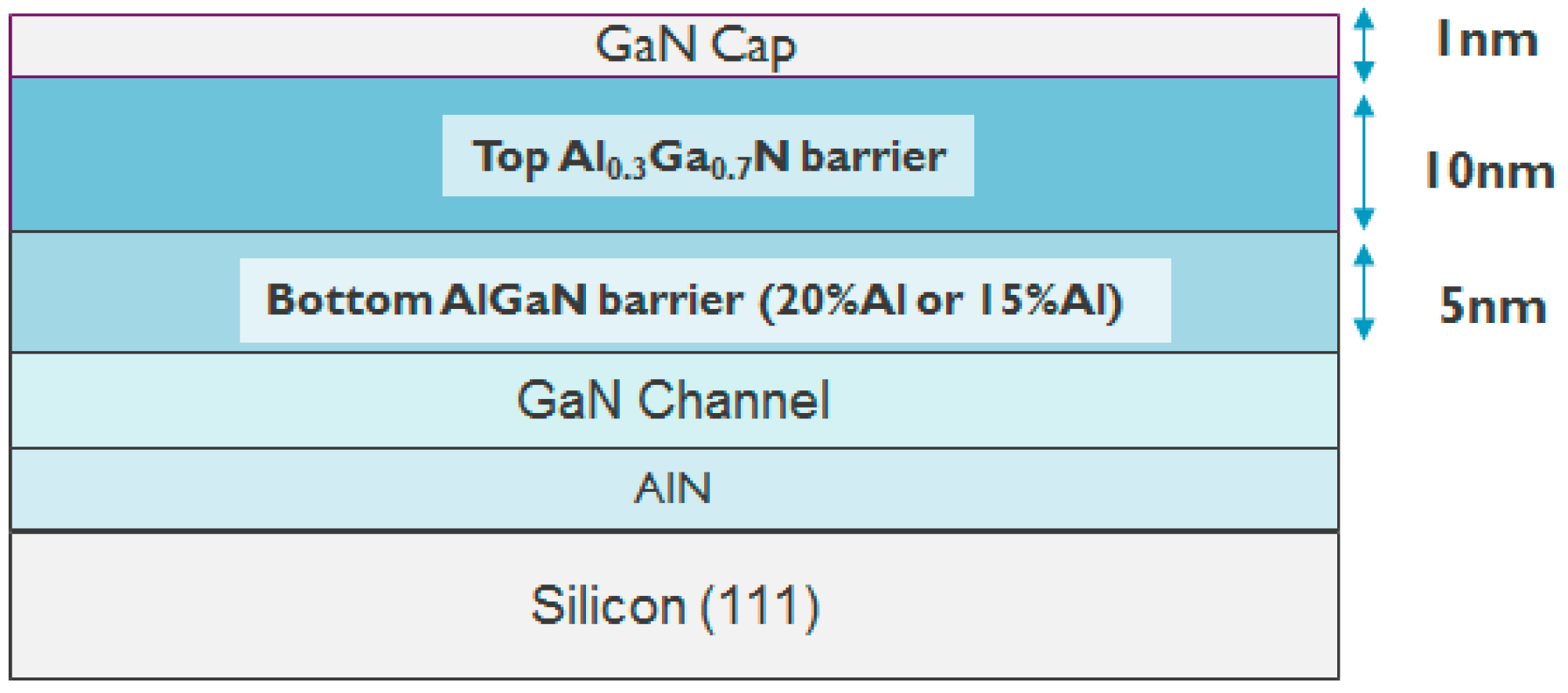
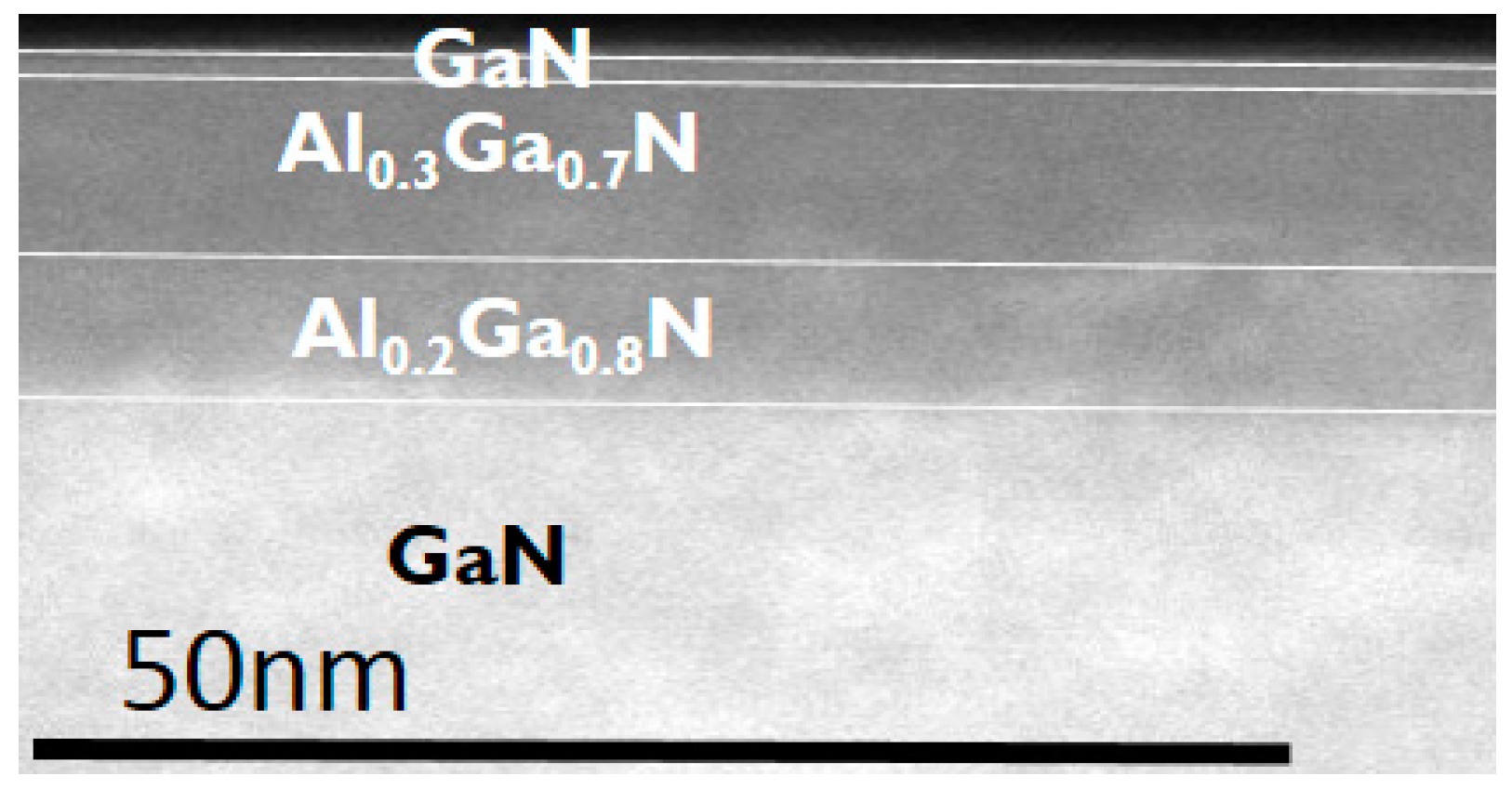
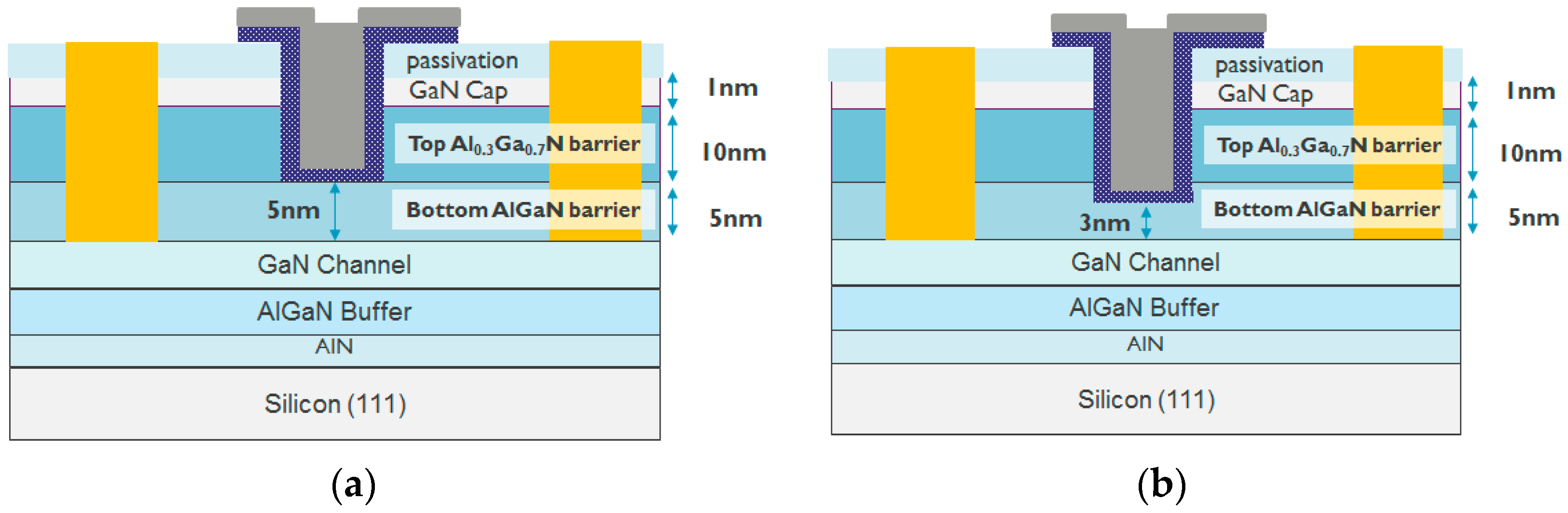
2. Device Fabrications
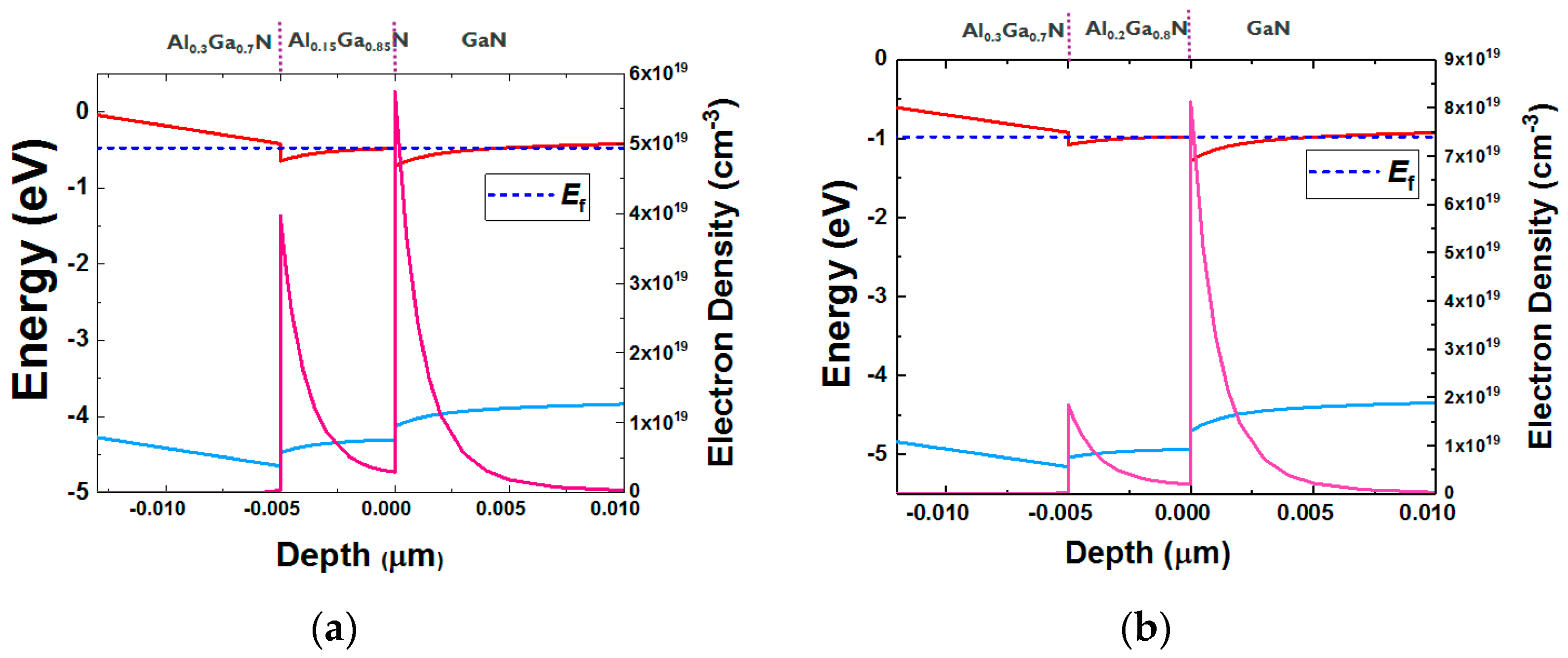
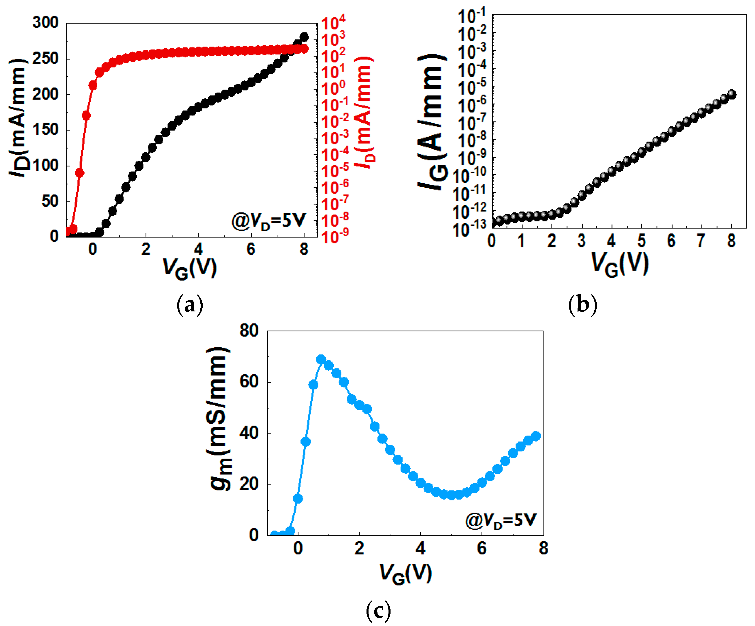
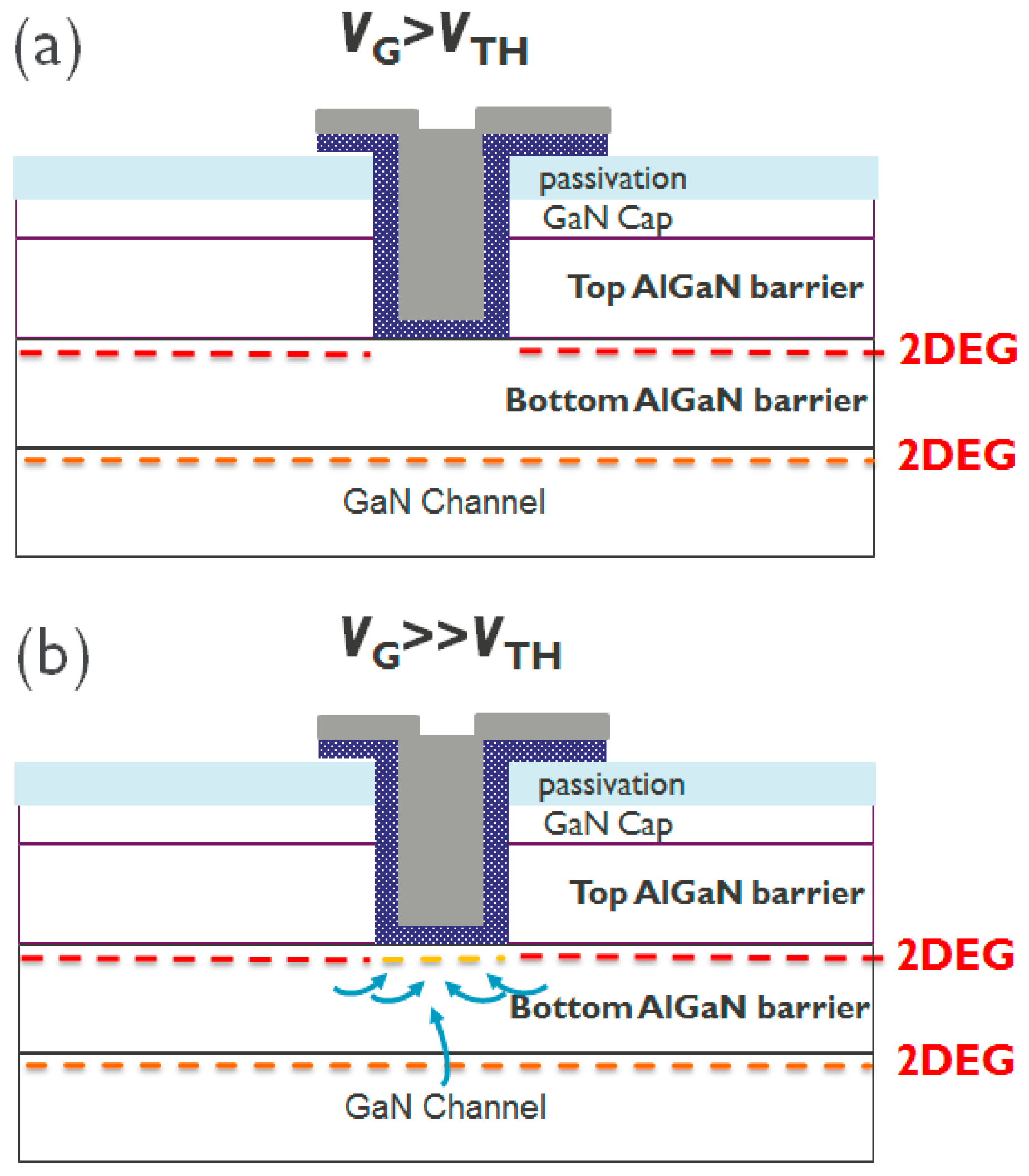
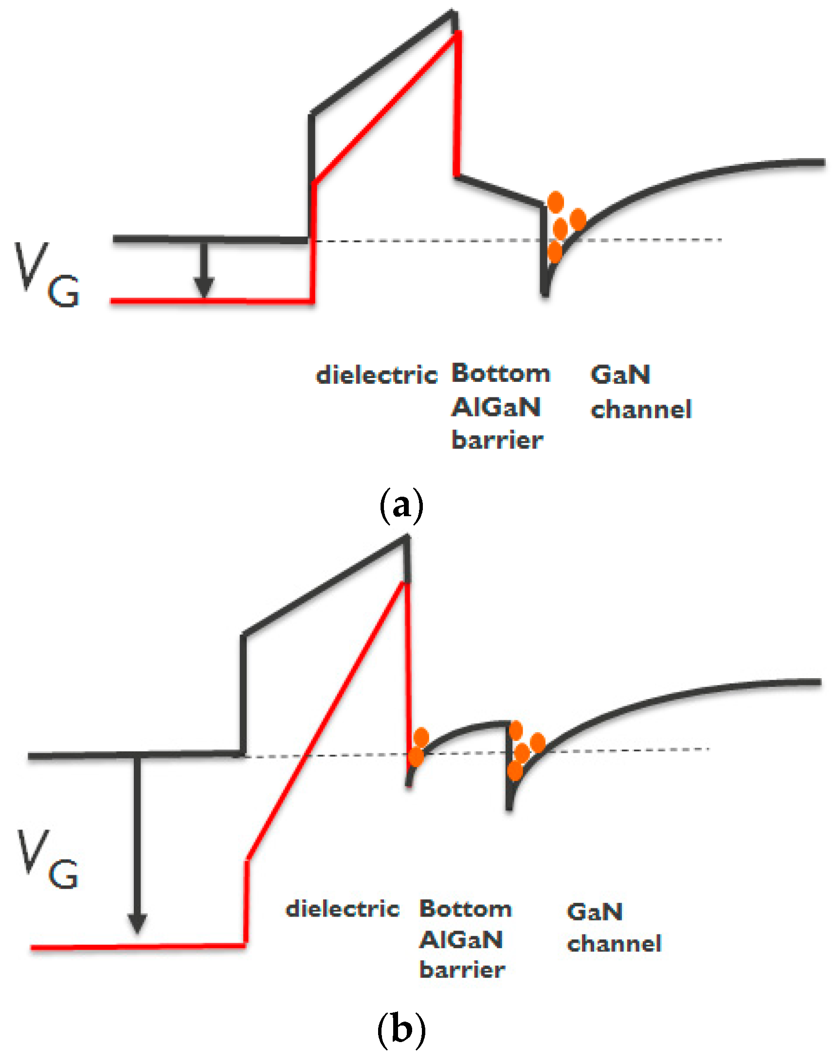
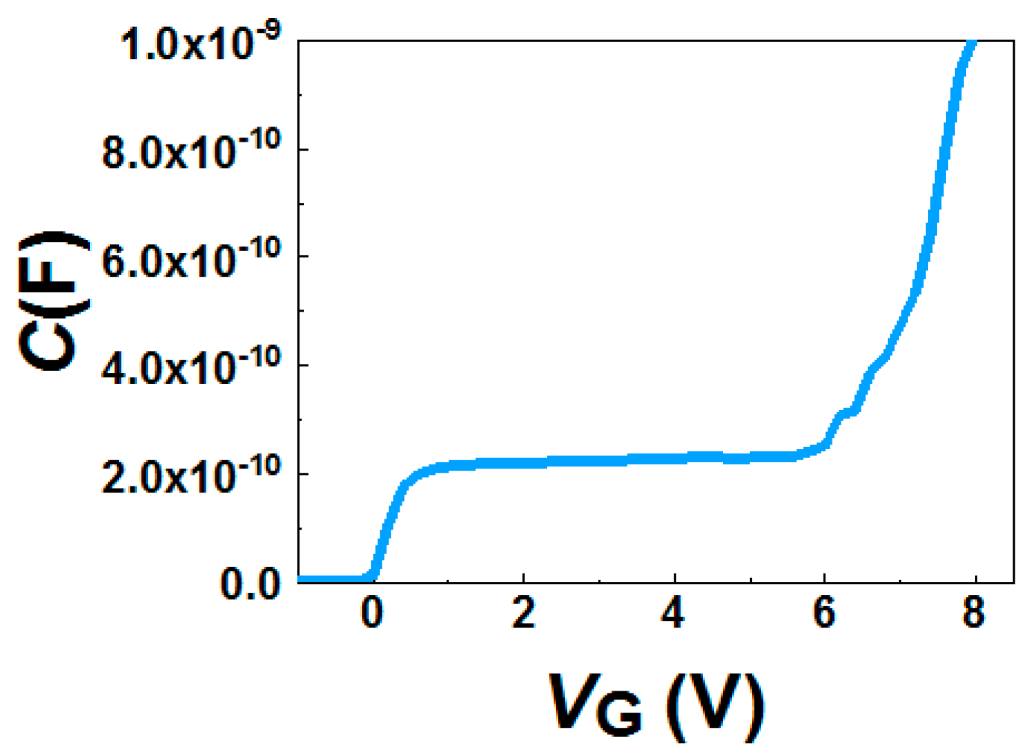
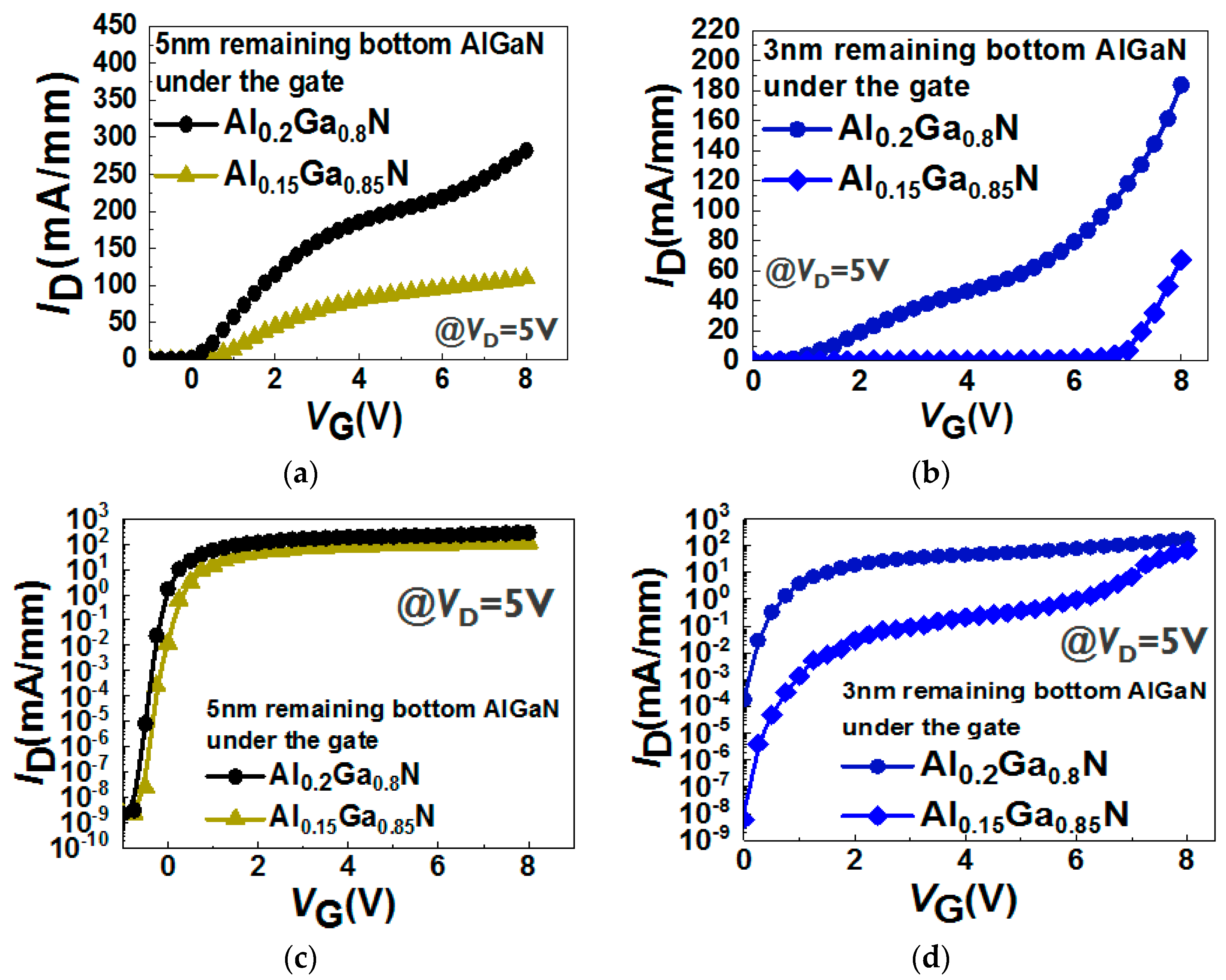
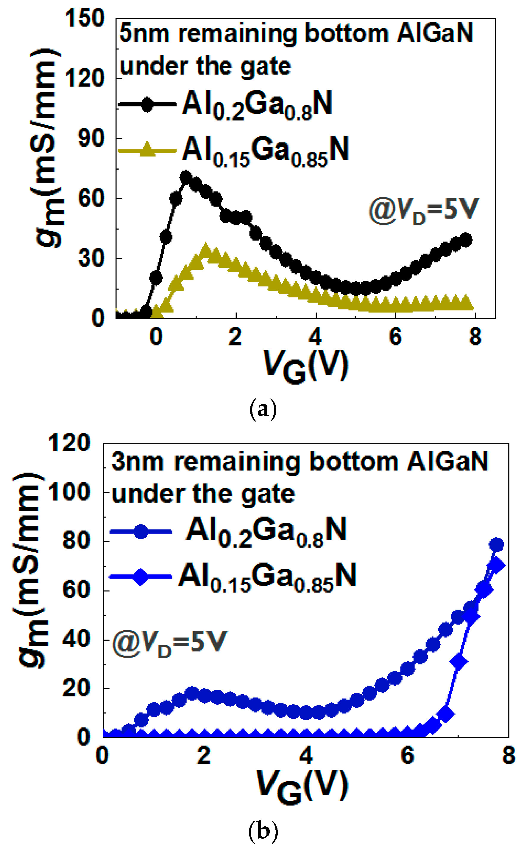
Figure 1 shows the schematic of the epitaxy structure in this study and Figure 2 shows an example of the transmission electron microscopy (TEM) image in an epitaxy structure with a double AlGaN barrier. This structure was grown by metal–organic chemical vapor deposition (MOCVD) on a silicon (111) substrate and consists of an AlN nucleation layer, a GaN channel, a bottom AlGaN barrier with two different Al contents (20% and 15%), a top AlGaN barrier with 30% Al content, and a 1 nm GaN cap. The Al% (20% and 30%) in AlGaN barrier is calibrated with the XPS by using a single AlGaN barrier hetero-structure. The calibrated growing conditions in MOCVD are used for the double AlGaN barrier hetero-structure. Figure 3 shows the simulated band diagram with the double AlGaN barriers, clearly indicating the existence of the electrons in the interface between top AlGaN/bottom AlGaN and bottom AlGaN/GaN. The recessed gate structure was formed by reactive ion etching (RIE). In order to control the etching depth, low etching rate of 5Å/sec is achieved by the mixed BCl3 (10 sccm)/Cl2 (15 sccm) gas. A gate recessed process is performed and a 15-nm Plasma-enhanced chemical vapor deposition (PECVD) Si3N4 is deposited as a surface passivation layer in the access region and a gate dielectric. TiN is used as the gate metal. The Ti/Al-based Au-free Ohmic contacts were formed by etching the Si3N4 layers and etching the AlGaN barrier. This was followed by annealing at 600 °C for 1 min in N2, resulting in 1 ohm.mm of Rc (contact resistance). Figure 4 shows the schematic of recessed gate MIS-HEMTs with a double AlGaN barrier. The important varied parameters are summarized in Table 1. The devices with Lg = 1 um, Lgs = 2 um, and Lgd = 6 um are fabricated for electrical characterizations.

3. Results

In the case of devices with a 5 nm remaining bottom AlGaN barrier under the gate area, a gate recess process is performed to etch until it reaches the surface of the bottom AlGaN barrier (Figure 4a). The IDVG, IG-VG, and gmVG characteristics are shown in Figure 5. Note that all IDVG characteristics in this work are measured from a lower VG till a higher VG. A double hump of gmVG characteristic is observed in Figure 5c, which is similar to the literature [15,16,17,18]. The double hump of gmVG characteristics in these references [15,16,17,18] arises from a shrinking of the depletion region below the gate, due to the depletion-mode characteristics. In our case, the recessed gate AlGaN/GaN MIS-HEMTs has a double barrier design. A double channel model that considers the electron transfer from the bottom channel to the top channel is proposed to explain the double hump gm-VG characteristics. First of all, once the VG is larger than VTH, the bottom channel is gradually turned on (Figure 6a and Figure 7a), resulting in a first gm peak as shown in Figure 5c. It is worth noting that at this stage the top channel from source to drain is initially disconnected below the gate dielectric due to a recessed gate process. However, when the VG is above 5 V, the top channel could be connected again, as shown in Figure 6b. In this scenario, the electrons can be transferred from the lateral 2DEG channel in the access region and/or interface below the bottom AlGaN barrier to the interface between the dielectric and the bottom AlGaN barrier [20,21] (Figure 7b). Then, the electrons can be accumulated under the gate dielectric [20,22]. This leads to the formation of the second channel under the gate, further connecting the source and drain to form the top channel leading to a second gm peak (Figure 5c).
Figure 8 shows an example of Capacitance-Voltage (CV) measurement in the device with 3 nm remaining bottom Al0.15Ga0.85N barrier. The capacitance is increase when the gate voltage is larger than 0 V, indicating the formation of the first channel (Figure 6a and Figure 7a). Once the gate voltage is applied larger enough, the capacitance is increased again, which is mainly due to the formation of the channel between dielectric and bottom AlGaN barrier (Figure 6b and Figure 7b), consistent with the reported literature [19].
Figure 9 shows the IDVG characteristics in the devices with different Al% content (Al0.2Ga0.8N and Al0.15Ga0.85N) in the bottom barriers and two different recessed depths (5 nm and 3 nm bottom AlGaN thickness under the gate area). The ID decreases but the VTH increases with a thinner remaining bottom AlGaN barrier (Figure 9b). Furthermore, the subthreshold slope (SS) is increased once the Al% in the bottom AlGaN barrier is decreased, which is mainly due to the low electron density in the channel between bottom AlGaN/GaN. By designing with 3nm remaining bottom Al0.15Ga0.85N barrier under the gate region, VTH ~3.25 V is achieved (VTH is defined at VG of ID = 0.1 mA/mm).
Figure 10 shows the gmVG characteristics in the devices with different Al% content (Al0.2Ga0.8N and Al0.15Ga0.85N) in the bottom barriers and two different recessed depths (5 nm and 3 nm bottom AlGaN thickness under the gate area). In the case of the devices with a 5 nm remaining bottom AlGaN barrier, lowering the Al% in the bottom AlGaN barrier decreases the gm peaks (Figure 10a). Furthermore, double hump gmVG characteristics can still be observed in the device with a 3 nm remaining bottom Al0.2Ga0.8N barrier under the gate region. First, the first gm peak decreases with a thinner remaining bottom AlGaN barrier under the gate dielectric, suggesting that the remaining bottom AlGaN barrier under the gate region limits the current contribution from the bottom channel. Second, the gm increases after 4 V in the device with a 3 nm remaining bottom Al0.2Ga0.8N barrier under the gate region (Figure 10b). Whereas, the gm increases after 5 V in the devices with a 5 nm remaining bottom Al0.2Ga0.8N barrier under the gate region (Figure 10a). This is in agreement with the model proposed above: Due to a thinner AlGaN barrier, a lower gate voltage can allow the electrons to transfer from the bottom channel to the area below the gate. Third, the second gm is higher than the first gm in the devices with a 3 nm remaining bottom AlGaN barrier under the gate region (Figure 10b). However, the first gm is higher than the second gm in the devices with a 5 nm remaining bottom AlGaN barrier under the gate region (Figure 10a). These observations suggest that the main current contribution in the devices with a 5 nm remaining bottom AlGaN barrier under the gate region is the bottom channel. However, in the devices with a 3 nm remaining bottom AlGaN barrier under the gate region, the main current contribution is derived from the top channel.
Table 2 summarizes the comparisons of this work with other recent reports in double channel HEMTs, indicating our work shows the promising characteristics in terms of Ion/Ioff ratio and VTH toward an enhancement mode characteristic.

4. Conclusions

In summary, recessed gate AlGaN/GaN MIS-HEMTs with double AlGaN barrier designs are investigated and discussed. A double hump of the gmVG characteristic can be observed in the recessed gate AlGaN/GaN MIS-HEMTs with double AlGaN barrier designs. A physical model is proposed to explain the double channel characteristics, which is mainly due to the formation of the top channel under a high VG bias. Once the gate voltage is applied at a high enough level, the top channel is formed, leading to an increase in drain current due to the current contribution from the top channel. Furthermore, by lowering the Al% in the bottom AlGaN barrier, the devices show a more positive VTH with the same recessed depth, indicating that a double AlGaN barrier design in recessed gate MIS-HEMTs can be an alternative strategy to achieve an enhancement mode characteristic.

Author Contributions

Data curation, T.-L.W., S.-W.T., and H.-J.J.; writing—original draft preparation, T.-L.W.; writing—review and editing, T.-L.W., S.-W.T., and H.-J.J. All authors have read and agreed to the published version of the manuscript.

Funding

This work was financially supported by the “Center for the Semiconductor Technology Research” from the Featured Areas Research Center Program within the framework of the Higher Education Sprout Project by the Ministry of Education (MOE) in Taiwan. It is also supported in part by the Ministry of Science and Technology, Taiwan, under Grant MOST-108-3017-F-009-003, MOST-106-2218-E-009-025-MY3 and by the Young Scholar Fellowship Program under Grant MOST 108-2636-E-009-006.

Conflicts of Interest

The authors declare no conflict of interest.

References

  1. Amano, H.; Baines, Y.; Beam, E.; Borga, M.; Bouchet, T.; Chalker, P.R.; Charles, M.; Chen, K.J.; Chowdhury, N.; Chu, R.; et al. The 2018 GaN power electronics roadmap. J. Phys. D Appl. Phys. 2018, 51, 1–48. [Google Scholar] [CrossRef]
  2. Chen, K.J.; Häberlen, O.; Lidow, A.; Tsai, C.L.; Ueda, T.; Uemoto, Y.; Wu, Y. GaN-on-Si power technology: Devices and applications. IEEE Trans. Electron Devices 2017, 64, 779–795. [Google Scholar] [CrossRef]
  3. Van Hove, M.; Boulay, S.; Bahl, S.R.; Stoffels, S.; Kang, X.; Wellekens, D.; Geens, K.; Delabie, A.; Decoutere, S. CMOS Process-Compatible High-Power Low-Leakage AlGaN/GaN MISHEMT on Silicon. IEEE Electron Device Lett. 2012, 33, 667–669. [Google Scholar] [CrossRef]
  4. Moens, P.; Liu, C.; Banerjee, A.; Vanmeerbeek, P.; Coppens, P.; Ziad, H.; Constant, A.; Li, Z.; de Vleeschouwer, H.; RoigGuitart, J.; et al. An Industrial Process for 650 V Rated GaN-on-Si Power Devices Using in-Situ SiN as a Gate Dielectric. In Proceedings of the International Symposium on Power Semiconductor Devices and ICs (ISPSD), Waikoloa, HI, USA, 15–19 June 2014; pp. 374–377. [Google Scholar] [CrossRef]
  5. Hua, M.; Zhang, Z.; Wei, J.; Lei, J.; Tang, G.; Fu, K.; Cai, Y.; Zhang, B.; Chen, K.J. Integration of LPCVD-SiNx Gate Dielectric with Recessed-Gate E-Mode GaN MIS-FETs: Toward High Performance, High Stability and Long TDDB Lifetime. In Proceedings of the IEEE International Electron Devices Meeting (IEDM), San Francisco, CA, USA, 3–7 December 2016; pp. 10.4.1–10.4.4. [Google Scholar] [CrossRef]
  6. Wu, T.-L.; Marcon, D.; de Jaeger, B.; van Hove, M.; Bakeroot, B.; Lin, D.; Stoffels, S.; Kang, X.; Roelofs, R.; Groeseneken, G.; et al. The Impact of the Gate Dielectric Quality in Developing Au-Free D-Mode and E-Mode Recessed Gate AlGaN/GaN Transistors on a 200 mm Si Substrate. In Proceedings of the International Symposium on Power Smicond Devices and ICs (ISPSD), Hong Kong, China, 10–14 May 2015; pp. 225–228. [Google Scholar] [CrossRef]
  7. De Jaeger, B.; van Hove, M.; Wellekens, D.; Kang, X.; Liang, H.; Mannaert, G.; Geens, K.; Decoutere, S. Au-Free CMOS-Compatible AlGaN/GaN HEMT Processing on 200 mm Si Substrates. In Proceedings of the 2012 24th International Symposium on Power Semiconductor Devices and ICs, Bruges, Belgium, 3–7 June 2012; pp. 49–52. [Google Scholar] [CrossRef]
  8. Wu, T.-L.; Marcon, D.; You, S.; Posthuma, N.; Bakeroot, B.; Stoffels, S.; van Hove, M.; Groeseneken, G.; Decoutere, S. Forward bias gate breakdown mechanism in enhancement-mode p-GaN gate AlGaN/GaN high-electron mobility transistors. IEEE Electron Device Lett. 2015, 36, 1001–1003. [Google Scholar] [CrossRef]
  9. Cai, Y.; Zhou, Y.; Chen, K.J.; Lau, K.M. High-performance enhancement-mode AlGaN/GaN HEMTs using fluoride-based plasma treatment. IEEE Electron Device Lett. 2005, 26, 435–437. [Google Scholar] [CrossRef]
  10. Huang, W.; Khan, T.; Chow, T.P. Enhancement-mode n-channel GaN MOSFETs on p and n-GaN/sapphire substrates. IEEE Electron Device Lett. 2006, 27, 796–798. [Google Scholar] [CrossRef]
  11. Lu, B.; Saadat, O.I.; Palacios, T. High-performance integrated dual-gate AlGaN/GaN enhancement-mode transistor. IEEE Electron Device Lett. 2010, 31, 990–992. [Google Scholar] [CrossRef]
  12. Wang, R.; Wu, Y.; Chen, K.J. Gain improvement of enhancement-mode AlGaN/GaN high-electron-mobility transistors using dual-gate architecture. Jpn. J. Appl. Phys. 2013, 47, 2820. [Google Scholar] [CrossRef]
  13. Sheng, N.H.; Lee, C.P.; Chen, R.T.; Miller, D.L.; Lee, S.J. Multiple-Channel GaAs/AlGaAs High Electron Mobility Transistors. IEEE Electron Device Lett. 1985, 6, 307–310. [Google Scholar] [CrossRef]
  14. Gaska, R.; Shur, M.S.; Fjeldly, T.A.; Bykhovski, A.D. Two-channel AlGaN/GaN heterostructure field effect transistor for high power applications. J. Appl. Phys. 1999, 85, 3009–3011. [Google Scholar] [CrossRef]
  15. Chu, R.; Zhou, Y.; Liu, J.; Wang, D.; Chen, K.J.; Lau, K.M. AlGaN-GaN Double-Channel HEMTs. IEEE Trans. Electron Devices 2005, 52, 438–446. [Google Scholar] [CrossRef]
  16. Palacios, T.; Chini, A.; Buttari, D.; Heikman, S.; Chakraborty, A.; Keller, S.; DenBaars, S.P.; Mishra, U.K. Use of Double-Channel Heterostructures to Improve the Access Resistance and Linearity in GaN-Based HEMTs. IEEE Trans. Electron Devices 2006, 53, 562–565. [Google Scholar] [CrossRef]
  17. Kamath, A.; Patil, T.; Adari, R.; Bhattacharya, I.; Ganguly, S.; Aldhaheri, R.W.; Hussain, M.A.; Saha, D. Double-Channel AlGaN/GaN High Electron Mobility Transistor with Back Barriers. IEEE Electron Device Lett. 2012, 33. [Google Scholar] [CrossRef]
  18. Xue, J.; Zhang, J.; Zhang, K.; Zhao, Y.; Zhang, L.; Ma, X.; Li, X.; Meng, F.; Hao, Y. Fabrication and characterization of InAlN/GaN-based double-channel high electron mobility transistors for electronic applications. J. Appl. Phys. 2012, 111, 114513. [Google Scholar] [CrossRef] [Green Version]
  19. Wei, J.; Liu, S.; Li, B.; Tang, X.; Lu, Y.; Liu, C.; Hua, M.; Zhang, Z.; Tang, G.; Chen, K.J. Enhancement-Mode GaN Double-Channel MOS-HEMT with Low On-Resistance and Robust Gate Recess. In Proceedings of the IEEE International Electron Devices Meeting (IEDM), Washington, DC, USA, 7–9 December 2015; pp. 9.4.1–9.4.4. [Google Scholar] [CrossRef]
  20. Mizue, C.; Hori, Y.; Miczek, M.; Hashizume, T. Capacitance-Voltage Characteristics of Al2O3/AlGaN/GaN Structures and State Density Distribution at Al2O3/AlGaN Interface. Jpn. J. Appl. Phys. 2011, 50, 021001. [Google Scholar] [CrossRef]
  21. Wu, T.-L.; Marcon, D.; Ronchi, N.; Bakeroot, B.; You, S.; Stoffels, S.; van Hove, M.; Bisi, D.; Meneghini, M.; Groeseneken, G.; et al. Analysis of Slow De-trapping Phenomena after a Positive Gate Bias on AlGaN/GaN MIS-HEMTs with in-situ Si3N4/Al2O3 Bilayer Gate Dielectrics. Solid-State Electron. 2015, 103, 127–130. [Google Scholar] [CrossRef]
  22. Lagger, P.; Steinschifter, P.; Reiner, M.; Denifl, G.; Naumann, A.; Wilde, L.; Sundqvist, J.; Pogany, D.; Ostermaier, C. Role of the dielectric for the charging dynamics of the dielectric/barrier interface in AlGaN/GaN based metal-insulator-semiconductor structures under forward gate bias stress. Appl. Phys. Lett. 2014, 105, 033512. [Google Scholar] [CrossRef]
  23. Lee, J.-H.; Kim, J.-G.; Ju, J.-M.; Ahn, W.-H.; Kang, S.-H.; Lee, J.-H. AlInGaN/GaN double-channel FinFET with high on-current and negligible current collapse. Solid-State Electron. 2020, 164, 107678. [Google Scholar] [CrossRef]
  24. Deen, D.A.; Miller, R.A.; Osinsky, A.V.; Downey, B.P.; Storm, D.F.; Meyer, D.J.; Katzer, D.S.; Nepal, N. Polarization-mediated Debye-screening of surface potential fluctuations in dual-channel AlN/GaN high electron mobility transistors. Appl. Phys. Lett. 2016, 120, 235704. [Google Scholar] [CrossRef] [Green Version]
Figure 1. Schematic of the epitaxy structure with a double AlGaN barrier used in this study.
Micromachines 11 00163 g001
Figure 2. Transmission electron microscopy (TEM) images of the epitaxy structure with a double AlGaN barrier.
Micromachines 11 00163 g002
Figure 3. Simulated band diagrams with an Al0.3Ga0.7N/Al0.15Ga0.85N barrier (a) and an Al0.3Ga0.7N/Al0.2Ga0.8N barrier (b).
Micromachines 11 00163 g003
Figure 4. Schematic of device structures of recessed gate AlGaN/GaN MIS-HEMTs with a 5 nm remaining bottom AlGaN barrier under the gate region (a) and a 3 nm remaining bottom AlGaN barrier under the gate region (b).
Micromachines 11 00163 g004
Figure 5. IDVG (a), IGVG (b) and gmVG (c) characteristics in a recessed gate MIS-HEMTs with a 5nm remaining bottom Al0.2Ga0.8N barrier under the gate. By designing a 5 nm bottom AlGaN barrier with 20% Al content, VTH ~0 V is realized (VTH is defined at VG of ID = 0.1 mA/mm).
Micromachines 11 00163 g005
Figure 6. The schematic of proposed double channel model (a) when VG > VTH and (b) VG >>> VTH.
Micromachines 11 00163 g006
Figure 7. Schematic of the band diagram under (a) VG > VTH and (b) VG >> VTH.
Micromachines 11 00163 g007
Figure 8. Capacitance-Voltage (CV) measurement in the device with 3 nm remaining bottom Al0.15Ga0.85N barrier.
Micromachines 11 00163 g008
Figure 9. ID-VG in a linear scale (a,b) and a logarithmic scale (c,d) in the devices with 5 nm or 3 nm remaining bottom AlGaN layer under the gate region with different Al% in the bottom AlGaN barrier.
Micromachines 11 00163 g009
Figure 10. gmVG characteristics in the devices with a (a) 5 nm or (b) 3 nm remaining bottom AlGaN layer under the gate region with different Al% in the bottom AlGaN barrier.
Micromachines 11 00163 g010
Table 1. Summary of the Varied Parameters.
ParametersTop AlGaN BarrierBottom AlGaN Barrier
Thickness10 nm5 nm
Al%30%20%
15%
Recessed depth
Remaining bottom AlGaN barrier under the gate region5 nm
3 nm
Table 2. Reference for the double channel GaN HEMTs.
ReferenceBarrier designsIon/IoffSS
(mV/dec)
VTH (V)
@0.1mA/mm
1nd gm
(mS/mm)
2nd gm
(mS/mm)
Our workAl0.3Ga0.7N/Al0.2Ga0.8N/GaN
5nm remaining bottom Al0.2Ga0.8N
1.2 × 101180.7~068.939
Al0.3Ga0.7N/Al0.15Ga0.85N/GaN
5nm remaining bottom Al0.15Ga0.85N
4.8 × 101087.90.2534.87.6
Al0.3Ga0.7N/ Al0.2Ga0.8N /GaN
3nm remaining bottom Al0.2Ga0.8N
-153.10.518.890
Al0.3Ga0.7N/ Al0.15Ga0.85N /GaN
3nm remaining bottom Al0.15Ga0.85N
5.5 × 1010229.33.25-71.2
Kamath et al. [17]Al0.3Ga0.7N/GaN/Al0.15Ga0.75N/GaN--~−7.83489
Wei et al. [19]AlGaN/AlN/GaN/AlN with 1.5 nm over-etch upper GaN layer~109720.5170103
Lee et al. [23]AlGaN/GaN/AlGaN/GaN
Fin Structure
--0.2133-
Deen et al. [24]AlN/GaN/AlN/GaN--~−4190-

