Melt Blown Fiber-Assisted Solvent-Free Device Fabrication at Low-Temperature


Abstract
1. Introduction
2. Materials and Methods
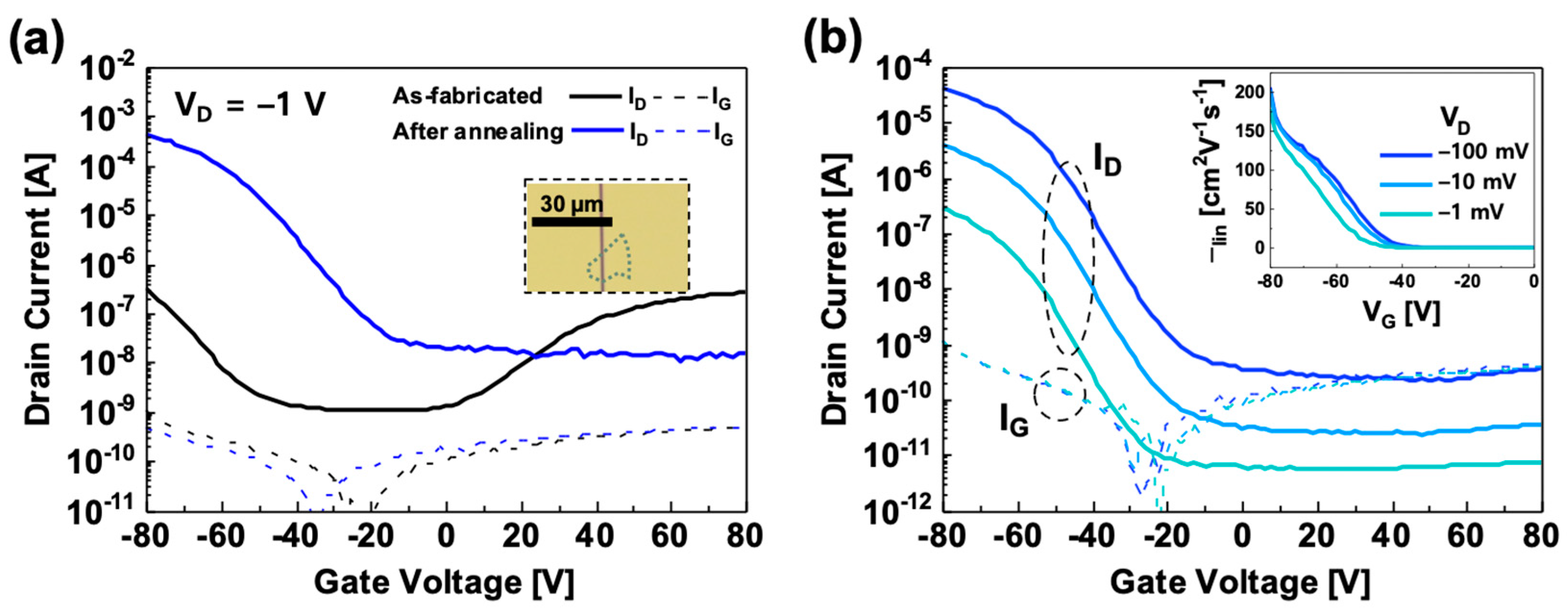
3. Results and Discussion
4. Conclusions
Supplementary Materials
Author Contributions
Funding
Conflicts of Interest
References
- Xia, Y.; Whitesides, G.M. Soft Lithography. Angew. Chem. Int. Ed. 1998, 37, 550–575. [Google Scholar] [CrossRef]
- Qin, D.; Xia, Y.; Whitesides, G.M. Soft lithography for micro- and nanoscale patterning. Nat. Protoc. 2010, 5, 491–502. [Google Scholar] [CrossRef] [PubMed]
- Sirringhaus, H.; Kawase, T.; Friend, R.H.; Shimoda, T.; Inbasekaran, M.; Wu, W.; Woo, E.P. High-Resolution Inkjet Printing of All-Polymer Transistor Circuits. Science 2000, 290, 2123–2126. [Google Scholar] [CrossRef] [PubMed]
- Noguchi, Y.; Sekitani, T.; Someya, T. Printed shadow masks for organic transistors. Appl. Phys. Lett. 2007, 91, 133502. [Google Scholar] [CrossRef]
- Muyres, D.V.; Baude, P.F.; Theiss, S.; Haase, M.; Kelley, T.W. Polymeric aperture masks for high performance organic integrated circuits. J. Vac. Sci. Technol. A 2004, 22, 1892. [Google Scholar] [CrossRef]
- Briseno, A.L.; Mannsfeld, S.C.B.; Ling, M.M.; Liu, S.; Tseng, R.J.; Reese, C.; Roberts, M.E.; Yang, Y.; Wudl, F.; Bao, Z. Patterning organic single-crystal transistor arrays. Nature 2006, 444, 913–917. [Google Scholar] [CrossRef]
- Yin, C.; Wang, X.; Chen, Y.; Li, D.; Lin, T.; Sun, S.; Shen, H.; Du, P.; Sun, J.; Meng, X.; et al. A ferroelectric relaxor polymer-enhanced p-type WSe2 transistor. Nanoscale 2018, 10, 1727–1734. [Google Scholar] [CrossRef]
- Allain, A.; Kis, A. Electron and Hole Mobilities in Single-Layer WSe2. ACS Nano 2014, 8, 7180–7185. [Google Scholar] [CrossRef]
- Movva, H.C.P.; Rai, A.; Kang, S.; Kim, K.; Fallahazad, B.; Taniguchi, T.; Watanabe, K.; Tutuc, E.; Banerjee, S.K. High-Mobility Holes in Dual-Gated WSe2 Field-Effect Transistors. ACS Nano 2015, 9, 10402–10410. [Google Scholar] [CrossRef]
- Fang, H.; Chuang, S.; Chang, T.C.; Takei, K.; Takahashi, T.; Javey, A. High-Performance Single Layered WSe2 p-FETs with Chemically Doped Contacts. Nano Lett. 2012, 12, 3788–3792. [Google Scholar] [CrossRef]
- Krasnozhon, D.; Lembke, D.; Nyffeler, C.; Leblebici, Y.; Kis, A. MoS2 Transistors Operating at Gigahertz Frequencies. Nano Lett. 2014, 14, 5905–5911. [Google Scholar] [CrossRef] [PubMed]
- Desai, S.B.; Seol, G.; Kang, J.-S.; Fang, H.; Battaglia, C.; Kapadia, R.; Ager, J.W.; Guo, J.; Javey, A. Strain-Induced Indirect to Direct Bandgap Transition in Multilayer WSe2. Nano Lett. 2014, 14, 4592–4597. [Google Scholar] [CrossRef] [PubMed]
- Liu, H.; Neal, A.T.; Ye, P.D. Channel Length Scaling of MoS2 MOSFETs. ACS Nano 2012, 10, 8563–8569. [Google Scholar] [CrossRef] [PubMed]
- Yun, H.; Lee, S.; Jung, D.; Lee, G.; Park, J.; Kwan, O.J.; Lee, D.J.; Park, C.Y. Removal of photoresist residues and healing of defects on graphene using H2 and CH4 plasma. Appl. Surf. Sci. 2019, 463, 802–808. [Google Scholar] [CrossRef]
- Liang, J.; Xu, K.; Toncini, B.; Bersch, B.; Jariwala, B.; Lin, Y.C.; Robinson, J.; Fullerton-Shirey, S.K. Impact of Post-Lithography Polymer Residue on the Electrical Characteristics of MoS2 and WSe2 Field Effect Transistors. Adv. Mater. Interfaces 2019, 6, 1801321. [Google Scholar] [CrossRef]
- Liu, H.; Si, M.; Najmaei, S.; Neal, A.T.; Du, Y.; Ajayan, P.M.; Lou, J.; Ye, P.D. Statistical Study of Deep Submicron Dual-Gated Field-Effect Transistors on Monolayer Chemical Vapor Deposition Molybdenum Disulfide Films. Nano Lett. 2013, 13, 2640–2646. [Google Scholar] [CrossRef]
- Das, S.; Chen, H.-Y.; Penumatcha, A.V.; Appenzeller, J. High Performance Multilayer MoS2 Transistors with Scandium Contacts. Nano Lett. 2013, 13, 100–105. [Google Scholar] [CrossRef]
- Xu, Y.; Cheng, C.; Du, S.; Yang, J.; Yu, B.; Luo, J.; Yin, W.; Li, E.; Dong, S.; Ye, P.; et al. Contacts between Two- and Three-Dimensional Materials: Ohmic, Schottky, and p–n Heterojunctions. ACS Nano 2016, 10, 4895–4919. [Google Scholar] [CrossRef]
- Allain, A.; Kang, J.; Banerjee, K.; Kis, A. Electrical contacts to two-dimensional semiconductors. Nat. Mater. 2005, 14, 1195–1205. [Google Scholar] [CrossRef]
- Seo, J.; Cho, K.; Lee, W.; Shin, J.; Kim, J.-K.; Kim, J.; Pak, J.; Lee, T. Effect of Facile p-Doping on Electrical and Optoelectronic Characteristics of Ambipolar WSe2 Field-Effect Transistors. Nanoscale Res. Lett. 2019, 14, 313. [Google Scholar] [CrossRef]
- Liu, B.; Ma, Y.; Zhang, A.; Chen, L.; Abbas, A.N.; Liu, Y.; Shen, C.; Wan, H.; Zhou, C. High-Performance WSe2 Field-Effect Transistors via Controlled Formation of In-Plane Heterojunctions. ACS Nano 2016, 10, 5153–5160. [Google Scholar] [CrossRef] [PubMed]
- Yamamoto, M.; Dutta, S.; Aikawa, S.; Nakaharai, S.; Wakabayashi, K.; Fuhrer, M.S.; Ueno, K.; Tsukagoshi, K. Self-Limiting Layer-by-Layer Oxidation of Atomically Thin WSe2. Nano Lett. 2015, 15, 2067–2073. [Google Scholar] [CrossRef] [PubMed]
- Yamamoto, M.; Nakaharai, S.; Ueno, K.; Tsukagoshi, K. Self-Limiting Oxides on WSe2 as Controlled Surface Acceptors and Low-Resistance Hole Contacts. Nano Lett. 2016, 16, 2720–2727. [Google Scholar] [CrossRef] [PubMed]


Publisher’s Note: MDPI stays neutral with regard to jurisdictional claims in published maps and institutional affiliations. |
© 2020 by the authors. Licensee MDPI, Basel, Switzerland. This article is an open access article distributed under the terms and conditions of the Creative Commons Attribution (CC BY) license (http://creativecommons.org/licenses/by/4.0/).
Share and Cite
Lee, M.; Kang, J.; Lee, Y.T. Melt Blown Fiber-Assisted Solvent-Free Device Fabrication at Low-Temperature. Micromachines 2020, 11, 1091. https://doi.org/10.3390/mi11121091
Lee M, Kang J, Lee YT. Melt Blown Fiber-Assisted Solvent-Free Device Fabrication at Low-Temperature. Micromachines. 2020; 11(12):1091. https://doi.org/10.3390/mi11121091
Chicago/Turabian StyleLee, Minjong, Joohoon Kang, and Young Tack Lee. 2020. "Melt Blown Fiber-Assisted Solvent-Free Device Fabrication at Low-Temperature" Micromachines 11, no. 12: 1091. https://doi.org/10.3390/mi11121091
APA StyleLee, M., Kang, J., & Lee, Y. T. (2020). Melt Blown Fiber-Assisted Solvent-Free Device Fabrication at Low-Temperature. Micromachines, 11(12), 1091. https://doi.org/10.3390/mi11121091