1. Introduction
Lithium niobate (LiNbO
3) is a crystalline dielectric material of considerable interest for its popular applications in optical communications and sensor systems [
1,
2,
3,
4]. Because of its attractive properties, such as its unique electro-optical effects, large nonlinear optical coefficients, high refractive index of 2.2, large transparent ranging from ultraviolet to infrared and excellent thermal stability, LiNbO
3 is referred as “silicon in nonlinear optics” [
5]. Traditionally, an LiNbO
3 wafer is processed by methods of slicing, grinding, etc. However, due to high hardness, it faces serious challenges including large chipping and poor-quality surface, which would lead to the reduction of product life [
6].
Ultrafast-laser material machining is promising in industrial products over conventional processing methods, without causing thermal damage. In order to improve processing precision and surface roughness, ultrafast laser machining in LiNbO
3 has been studied intensively in recent years [
7,
8,
9,
10,
11,
12]. Chen et al. measured the surface-ablation threshold of LiNbO
3, which decreases significantly along with an increase of the pulse number, until reaching a constant level due to an incubation effect [
10]. Fissi et al. reported that the micromachining rate strongly depends on the operating parameters, such as laser power, scanning speed, and scanning number. Besides, laser pulse overlap around 93% for LiNbO
3 helps to achieve optimal surface roughness [
11]. Javaux’s group observed the influence of number of subpusles in burst mode and repetition frequency on transparent materials. In loose focusing configuration, the use of burst mode allows for increasing the kerf width without extra energy absorption, and the kerf width increases when the laser repetition frequency decreases [
12].
According to our previous investigation on LiNbO
3 cutting, small chipping and smooth roughness have been achieved. However, it takes hundreds of laser passes to cut such a hard material through [
13]. It has been a key problem to process thick LiNbO
3 wafers at high speed while maintaining good quality. However, laser dicing is a potential for its high throughput and good-quality edges, which is capable of suppressing the mentioned problem. Laser dicing has attracted lots of attention on processing different semiconductor materials, such as silicon [
14] and glass [
15,
16,
17,
18,
19]. Nevertheless, there is minimal literature investigating the effect of picosecond-laser parameters on multiple characteristics in LiNbO
3 dicing using Taguchi method, which has been widely used in engineering to optimize the processing parameters and improve the yield and the reliability in machining a product by the means of orthogonal-array experiment design, analysis of variance (ANOVA) and signal to noise (S/N) ratio, etc.
In this paper, considering the robustness and cost-performance ratio of ultrafast laser systems, we employed a picosecond-laser experimental setup and made an orthogonal-array experimental design to study the influence of laser power, repetition frequency, number of subpulses, depth of each pass, and scanning velocity on LiNbO3 dicing characteristics. Using analysis of variance, the most influential processing parameter in LiNbO3 laser dicing was obtained. For instance, the number of subpulses plays a dominant role on chipping size and side roughness. By analysis of relations between different characteristics, kerf width, Sq roughness, and processing rate were chosen to evaluate the overall characteristics in LiNbO3 dicing. Finally, the optimal parameters for picosecond laser dicing were determined and applied to a LiNbO3 product, which was well processed with narrower width, less chipping, and smoother surface as well as efficiency increased by 10 times compared with conventional methods. Our picosecond-laser-dicing result reveals a great potential for end product of high-demanding processing.
3. Results
There are many processing parameters that may affect LiNbO
3 dicing characteristics, including the laser power, repetition frequency, number of subpulses, depth of each pass, and scanning velocity, symbolized by
p,
f,
n,
d, and
v, respectively. In this study, these five parameters and their four levels are considered and the level numbers of 1, 2, 3, and 4 are used in the following discussion, which stand for their levels from small-to-large value. Since the number of complete experimental trials is up to 1024, an orthogonal-array experiment design is made to effectively reduce the number of experimental trials [
20]. Based on the selected laser-dicing parameters and their levels,
Table 1 lists the adopted experiment design, which results in only 16 sets of experiment instead of 1024.
The processing accuracy, surface quality and productivity in LiNbO
3 wafers are of great importance due to their impact on the overall performance of the product. In this study, kerf width and chipping size in the top surface serve as processing accuracy, while the arithmetical mean roughness, the root mean square roughness, and the maximum roughness of side surface are used to evaluate surface quality. In addition, processing rate represents the productivity of laser dicing. Thus, the LiNbO
3 dicing characteristics are estimated with kerf width, chipping size, arithmetical mean roughness, root mean square roughness, maximum roughness, and processing rate, respectively, abbreviated as
W,
L,
Sa,
Sq,
Sz, and
R. Here,
W and
L of the top surface were measured using a 500X-magnified digital microscope (DM6B, Leica, Wetzlar, Germany) with an accuracy of 0.1 μm.
Sa,
Sq, and
Sz of the side surface were detected with a white surface interferometer (Zygo NewView8300, AMETEK, Ltd., New York, NY, USA).
R was calculated with the equation as Equation (1):
where
v,
d, and
t are scanning velocity, depth of each pass, and the sample thickness of 1 mm, respectively.
On the basis of the orthogonal-array experimental design listed in
Table 1, laser-dicing experiments on the LiNbO
3 sample were conducted.
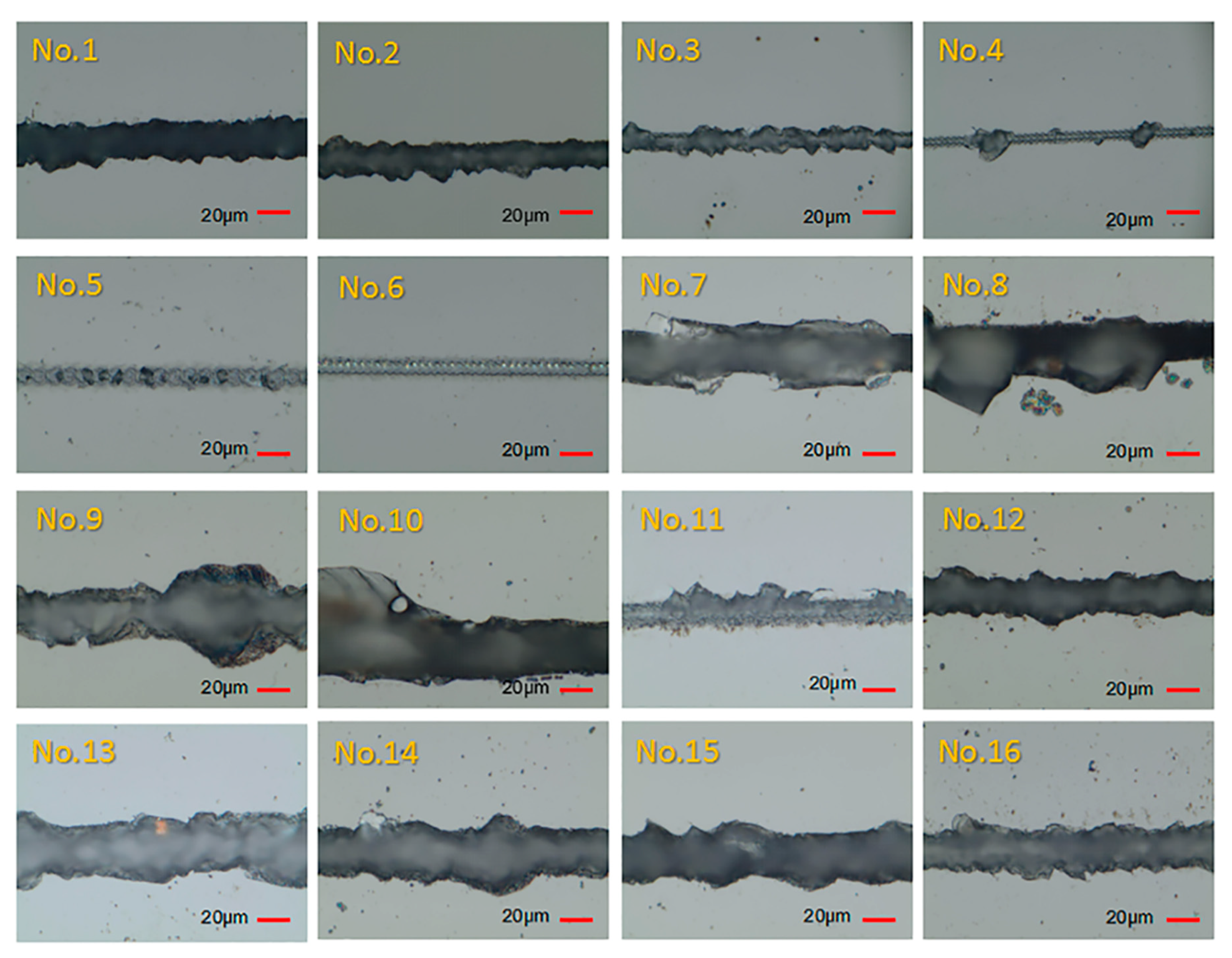
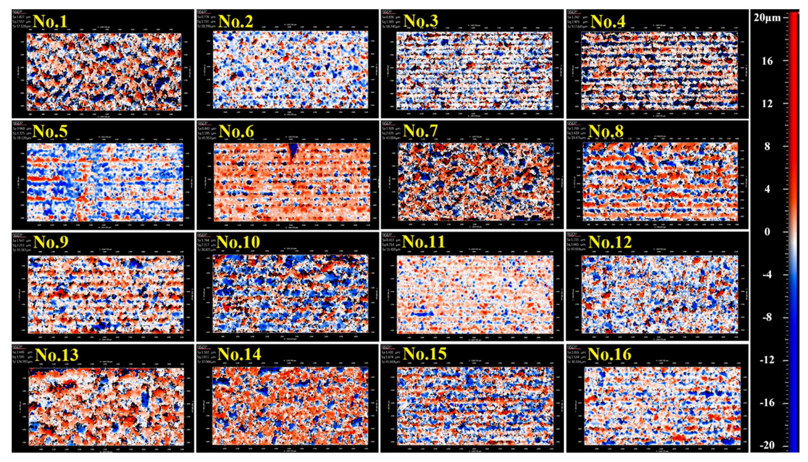
Figure 2 and
Figure 3, respectively, present the images in top and side surface of the laser-dicing samples under various parameters. The numbers in the figures correspond to experimental numbers in
Table 1 and indicate the experimental parameters for that particular sample. For each set of the experiment, the measurement of processing accuracy, surface roughness, and processing rate was conducted at four different points and the results were summarized in
Table 2. According to
Table 2, significant changes of cutting quality took place in our experimental design with a wide-ranged value of kerf width (4.6–37.9 μm), chipping size (4.8–42.2 μm),
Sa roughness (0.45–2.45 μm),
Sq roughness (0.71–3.60 μm),
Sz roughness (15.41–517.65 μm), and processing rate (2–20 mm/s). From
Figure 2, it is observed that bigger chippings occurring in No.8–No.10 and larger kerf width in No.13–No.15. Besides, some defects emerged in the side surface of No.1, No.4, No.7, No.10, No.13, and No.14 in
Figure 3.
4. Discussion
To obtain the most significant parameter for each cutting characteristic in LiNbO
3 dicing, analysis of variance was applied to obtain the individual significance of
p,
f,
n,
d, and
v, which is calculated by the decomposition of the variance using a Minitab 17 statistical software (Minitab Inc., State College, PA, USA) [
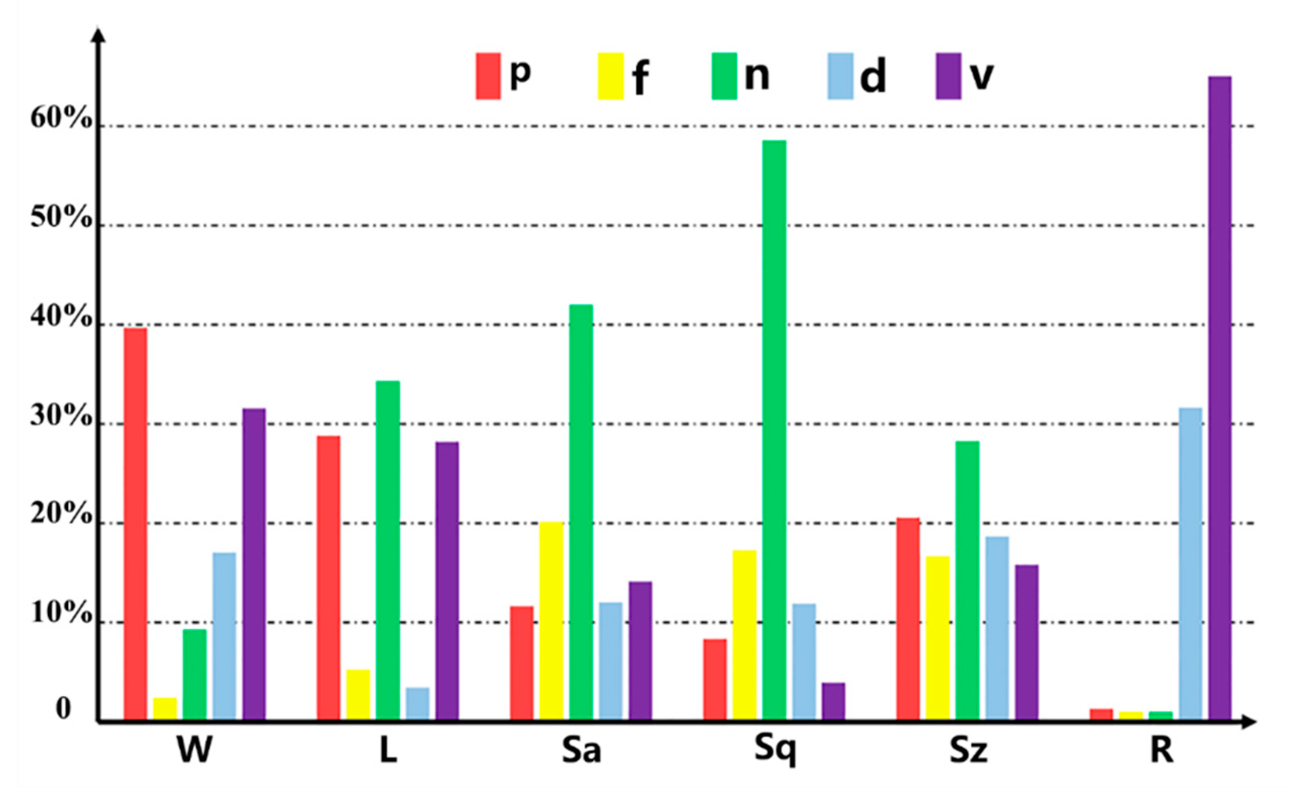
21]. Displayed in
Figure 4, the ANOVA result reveals that the percentages of contribution from each parameter is various and dependent on the LiNbO
3 characteristics in laser dicing. Both laser power and scanning velocity have significant effects on kerf width, and the factors account for 40% and 32% of the total variation, respectively. As for the edge chipping, number of subpulses becomes the main influencing parameter with a significant influence of 35% on chipping size. Besides, number of subpulses is still the dominant factor on
Sa,
Sq, and
Sz roughness in the side surface. In terms of processing rate, scanning velocity plays the most important role with a high contribution up to 62% and is followed by the depth of each pass, which is corresponding to Equation (1). When considering promoting the characteristics of
W,
L,
Sa,
Sq, and
Sz, the appropriate values of laser power, scanning velocity, as well as number of subpulses, must be chosen carefully because they emerge as the most influential experimental parameters in LiNbO
3 laser dicing. The kerf width and chipping size of the top surface are directly relative to the laser-damaged area. According to previous essays [
10], the diameter of the damaged area
D depends strongly on the maximum laser fluence
F0 and the material ablation-threshold
Fth, which is calculated by the following Equation (2):
where
ω0 is the laser beam radius. Increasing the laser power tends to increase the maximum laser fluence
F0, while increasing the scanning time tends to decrease the material ablation-threshold
Fth because of an increase in the pulse number applied to the surface. Thus, laser power and scanning velocity have significant effects on both kerf width and chipping size. Besides, compared with a single laser pulse, the absorption coefficient under burstmode laser pulse would increase due to the accumulation of laser-induced modification. For simplicity, when using burstmode laser pulse with
n subpulses, the modified absorptivity
can be estimated by Equation (3):
where
is the initial absorptivity and
is the increase of absorptivity induced by subsequent subpulse in burstmode laser. As a result, more defects in the intra volume of the sample are easy to appear in burst-mode laser machining and the side surface becomes rougher with a larger number of subpulses. It is recommended that better dicing quality can be obtained when using a lower laser power and a larger scanning velocity and smaller number of subpulses, but the laser power should be larger than the ablation threshold of LiNbO
3 material in order to cause laser-induced modification. On the other side, depth of each pass is less important for LiNbO
3 dicing quality, which implies processing rate can be enlarged reasonably by means of increasing the depth of each pass while maintaining a good quality of LiNbO
3 dicing.
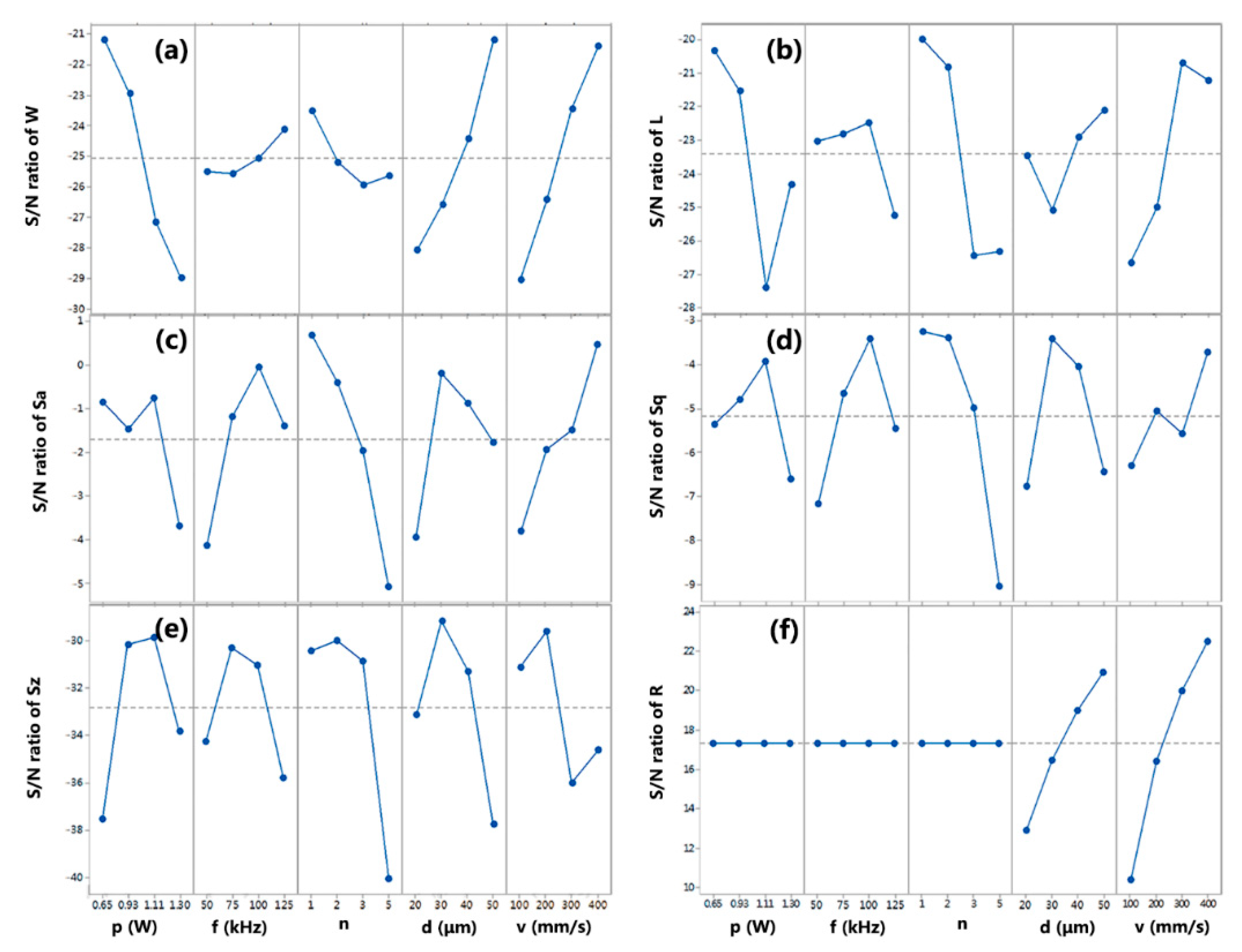
To investigate how the process parameters affect the cutting characteristics in laser dicing, the signal-to-noise (S/N) ratio is used to measure the variations of experimental result. The smaller values of
W,
L,
Sa,
Sq,
Sz are desired, However, the larger value of
R indicates the better performance. S/N ratios of
W,
L,
Sa,
Sq, and
Sz depending on the criterion of smaller-the-better are calculated by Equation (4):
while the S/N ratio of
R depending on the criterion of larger-the-better is given by Equation (5):
where
yi is the observed response value at the
i-th trail and n is the number of observations [
22]. Based on the larger S/N ratio criterion, the optimal level of the process parameters is the level with the highest S/N ratio in
Figure 5. For instance, the processing parameters of laser power at level 1, repetition frequency at level 4, number of subpulses at level 1, depth of each pass at level 4, and scanning velocity at level 4 yield the best result of kerf width. As a result, the value of
W is the smallest when using the parameter combination of
p1-
f4-
n1-
d4-
v4, which is corresponding to the mentioned theoretical discussion. Similarly, it can be concluded that the optimal parameter combination of levels for the smallest
L, and the lowest
Sa,
Sq,
Sz, are
p1-
f3-
n1-
d4-
v3,
p1-
f3-
n1-
d2-
v4,
p3-
f3-
n1-
d2-
v4,
p3-
f2-
n2-
d2-
v2, respectively. However, the optimal combination for the fastest
R is
d4-
v4, because processing rate only depends on scanning velocity and depth of each pass based on Equation (1). Since the best parameter combination for the six characteristics are different from each other, a tradeoff between processing accuracy, surface roughness, and processing rate in laser dicing is necessary.
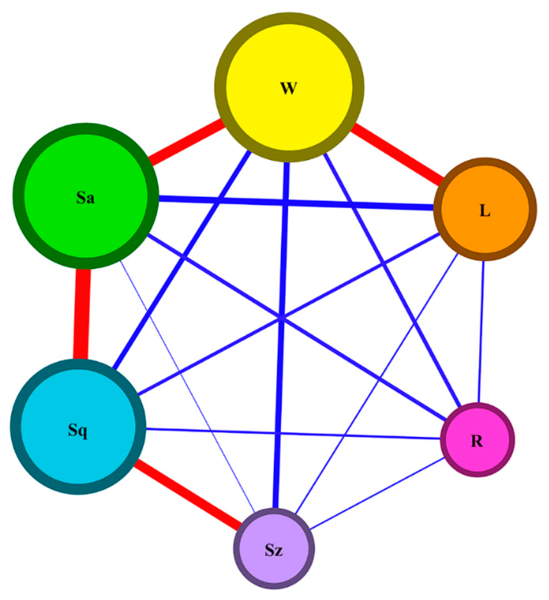
In order to determine the optimal parameter combination for the overall characteristic, the above six characteristics have to be degenerated and simplified. The analysis of mutual relations between kerf width, chipping size,
Sa,
Sq,
Sz of side roughness, and processing rate is applied with Pearson’s correlation coefficient. The coefficient is calculated by dividing the covariance of the two variables by the product of their standard deviations. When the coefficient is bigger than 0.5, it means the relation strength is large. The analysis result is shown in
Figure 6, wherein the thickness of the line indicates the value of the correlation coefficient and the size of circle indicates the sum of coefficients related. Because the correlations between processing rate and other characteristics are too weak, R must be an additional consideration. Fortunately, the correlation coefficients between
W,
L, and
Sa, as well as those between
Sq,
Sa, and
Sz, are bigger than 0.5. Thus,
W is strongly relative to
L and
Sa, meanwhile
Sq is significantly associated with
Sa and
Sz. It can be concluded that a good performance of
L,
Sa, and
Sz would be achieved with the optimal values of
W and
Sq. As a result, kerf width,
Sq roughness, and processing rate are selected as the representative characteristics in LiNbO
3 laser dicing. With the help of
Figure 4, laser power is the most important for
W, repetition frequency and number of subpulses are the most important for
Sa, and depth of each pass and scanning velocity are the most important for
R. According to
Figure 5, laser power at level 1 yields the optimal result of
W, repetition frequency at level 3 and number of subpulses at level 1 yield the optimal result of
Sq, and depth of each pass at level 4 and scanning velocity at level 4 yield the best result of
R. Based on the above analysis, the optimized parameter combination of levels for overall characteristic are determined as
p1-
f3-
n1-
d4-
v4. Therefore, a low laser power of 0.65 W, a high repetition frequency of 100 kHz, a small number of subpulses of 1, a large depth of each pass of 50 μm, and a fast scanning velocity of 400 mm/s are recommended to obtain better laser-dicing lithium niobate with high processing accuracy, smooth surface roughness, and large productivity.
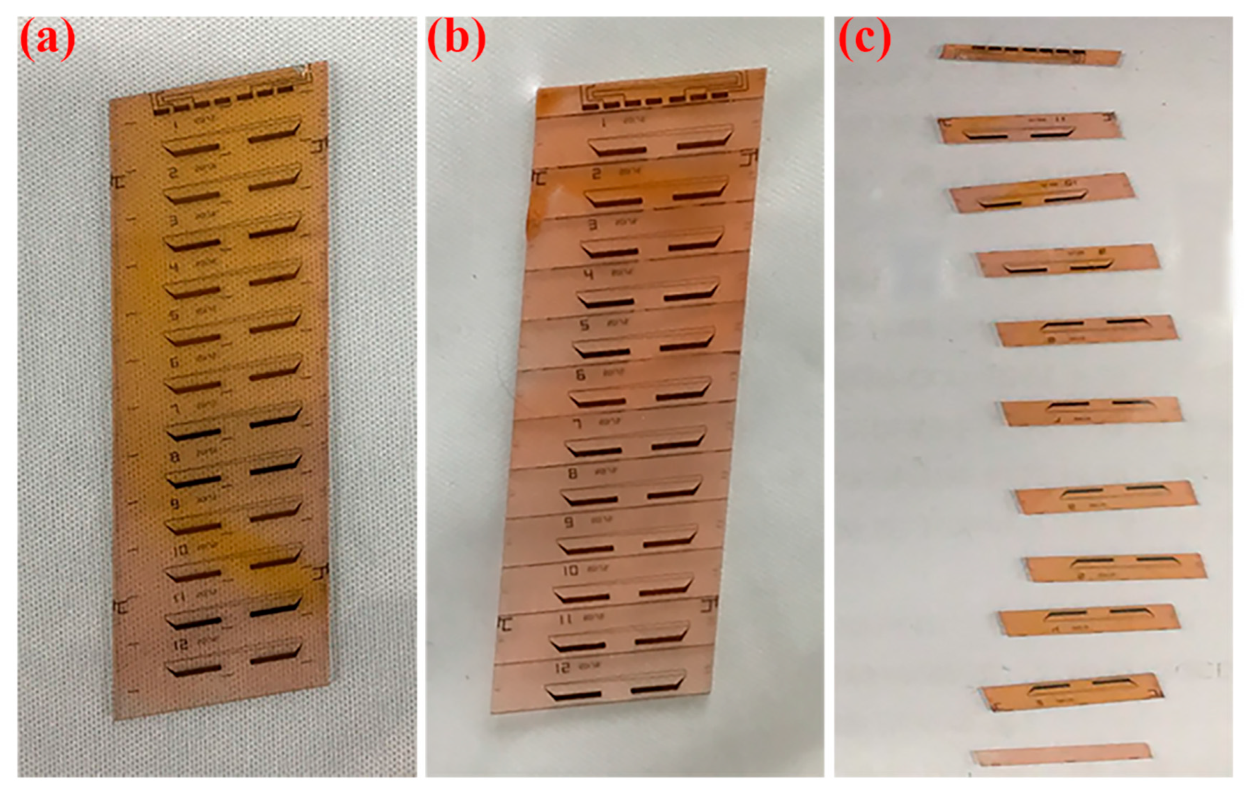
Shown in
Figure 7a, electro-optic waveguide modulators on a 1-mm thick LiNbO
3 wafer were applied in picosecond laser dicing with the optimal parameters of
p1-
f3-
n1-
d4-
v4, which are the products used in fiber optic gyroscope. To avoid the electro-optic waveguide modulators being polluted, photoresist was used to protect them from debris during machining, and laser dicing started from the reverse surface of the wafer. The LiNbO
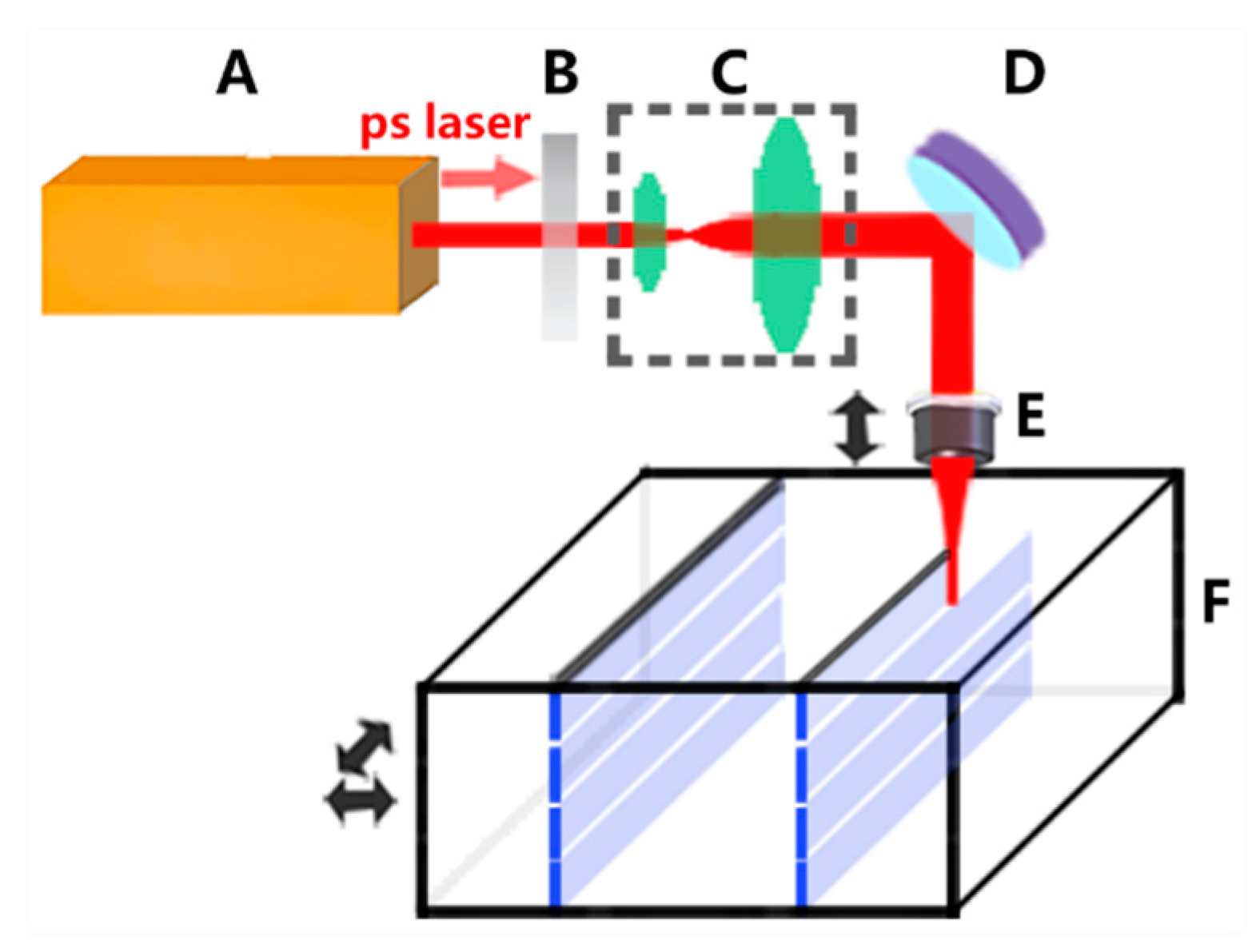
3 wafer was fixed on the X/Y-axis stages and processed in the experimental setup illustrated in
Figure 1. The picosecond laser system was operated in single pulse mode with laser power as 0.65 W and repetition rate as 100 kHz. In addition, the wafer was fed through the laser beam with a speed of 400 mm/s, and 20 passes were taken with 50-μm depth of each pass to cover the wafer thickness.
Figure 7b presents the image of the wafer after lasing dicing. Then, under mechanical stress, the wafer was divided into a dozen electro-optic waveguide modulators in
Figure 7c.
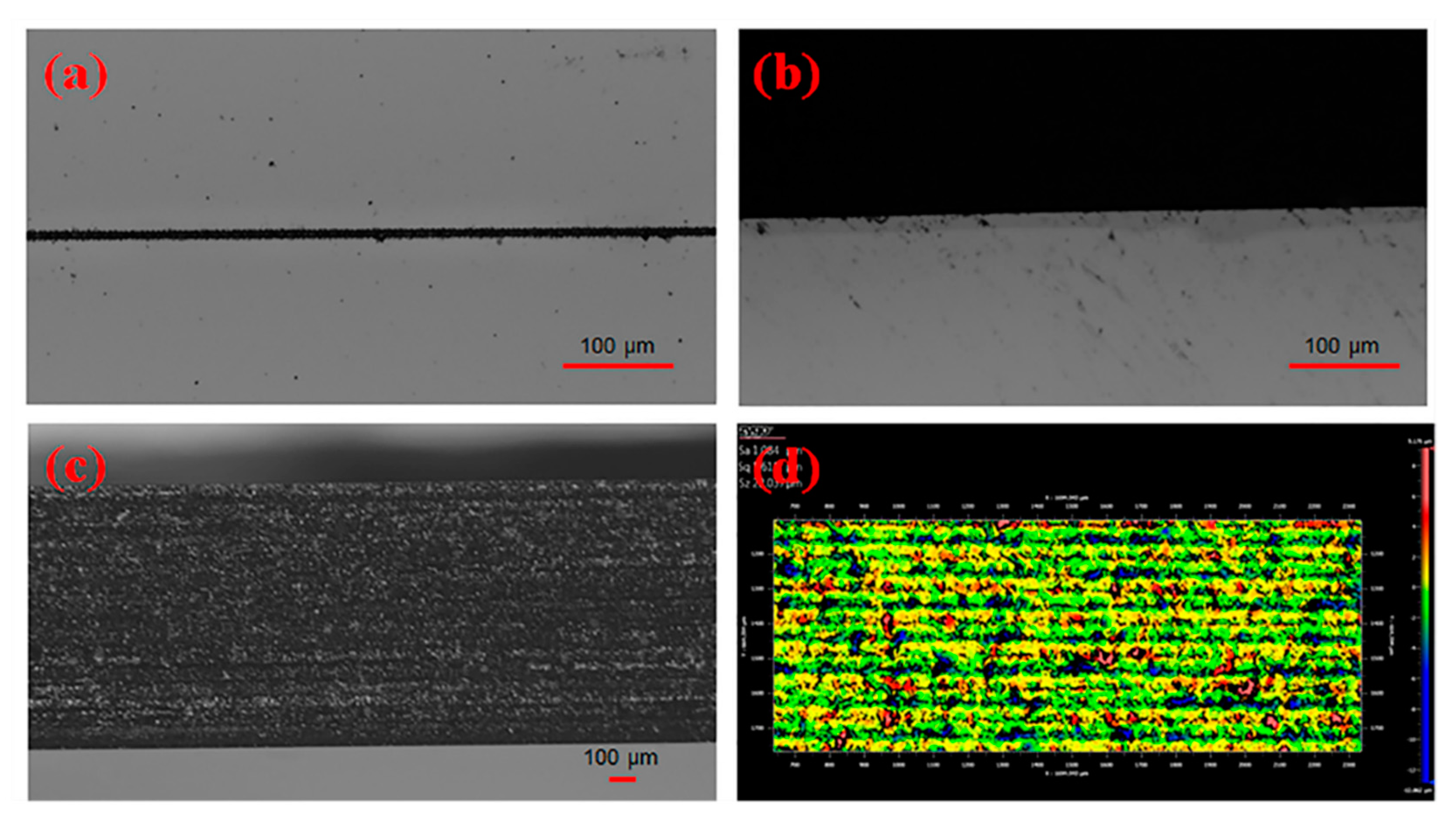
Figure 8a,b show the top surface of the wafer before and after the breaking process, meanwhile kerf width and chipping size are small as 7.5 μm and 5.8 μm, respectively. Less defects at the side surface could be identified in
Figure 8c, and it was further examined by white surface interferometer with an
Sa of 1.08 μm,
Sq of 1.61 μm, and
Sz of 22.04 μm in
Figure 8d. Moreover, it consumed about 3 min per wafer dicing instead of half an hour when using conventional methods, which implied that the processing rate of laser dicing was increased by an order of magnitude. Besides, the best-performance sample in
Table 2 is No.5 using the processing parameter combination of
p2-
f1-
n2-
d3-
v4 with 9.1 μm (
W), 6.3 μm (
L), 0.96 μm (
Sa), 1.33 μm (
Sq), 28.12 μm (
Sz), and 16 mm/s (
R). Because we decreased the laser power, reduced the number of subpulses and increased the depth of each pass, the final application was better than No.5 sample in
Table 2 with a narrower kerf width, a smaller chipping, and a higher productivity. Thus, the method of laser dicing is promising in processing the thick wafer, which needs both good quality and high efficiency.


