Vertical Leakage in GaN-on-Si Stacks Investigated by a Buffer Decomposition Experiment


 ,
,  , ,
, ,  and
and 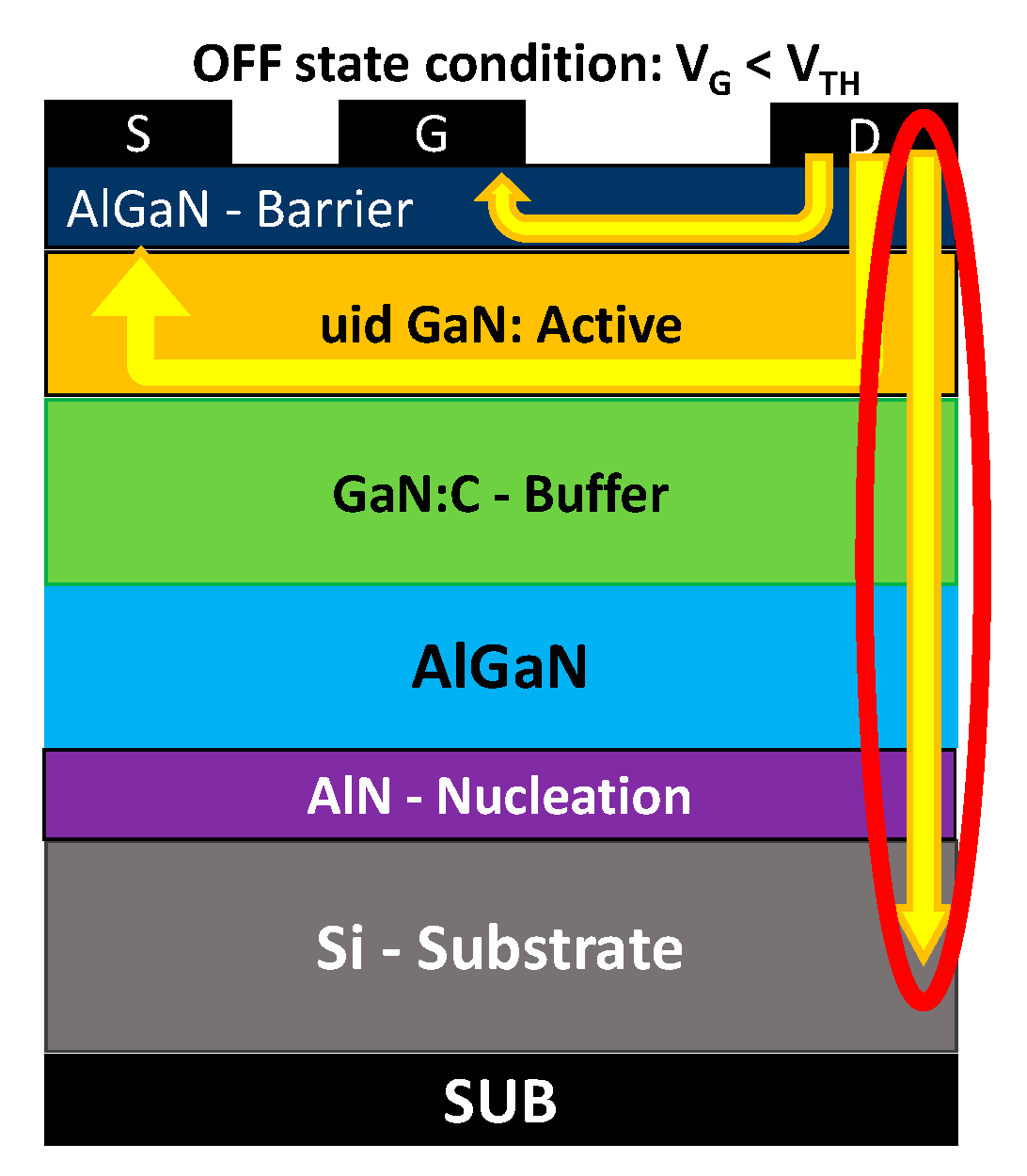
Abstract
1. Introduction
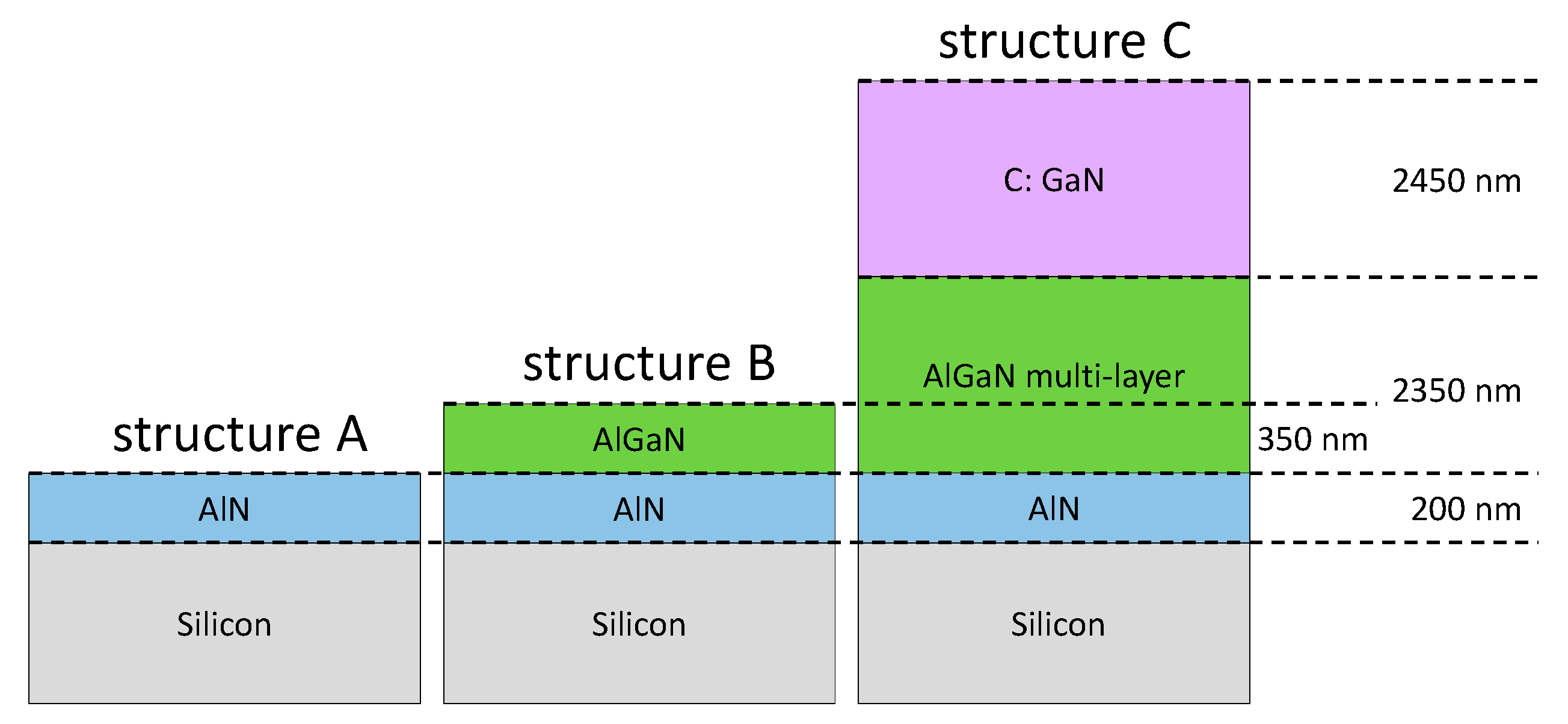
2. Experimental Details
3. Results and Discussion
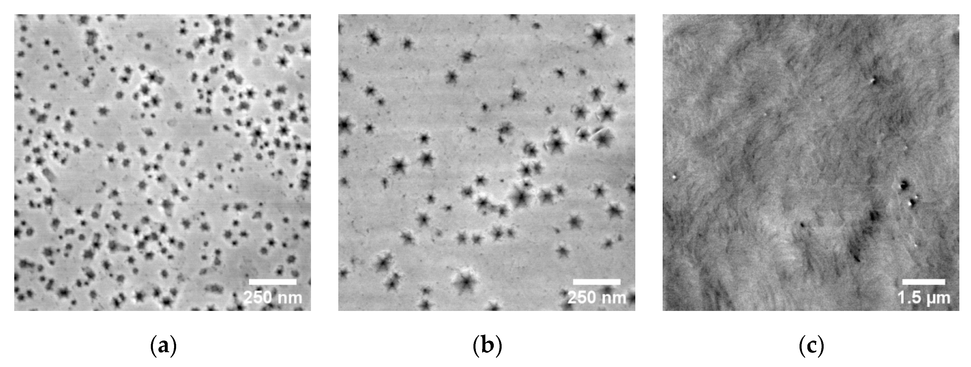
3.1. Material Quality
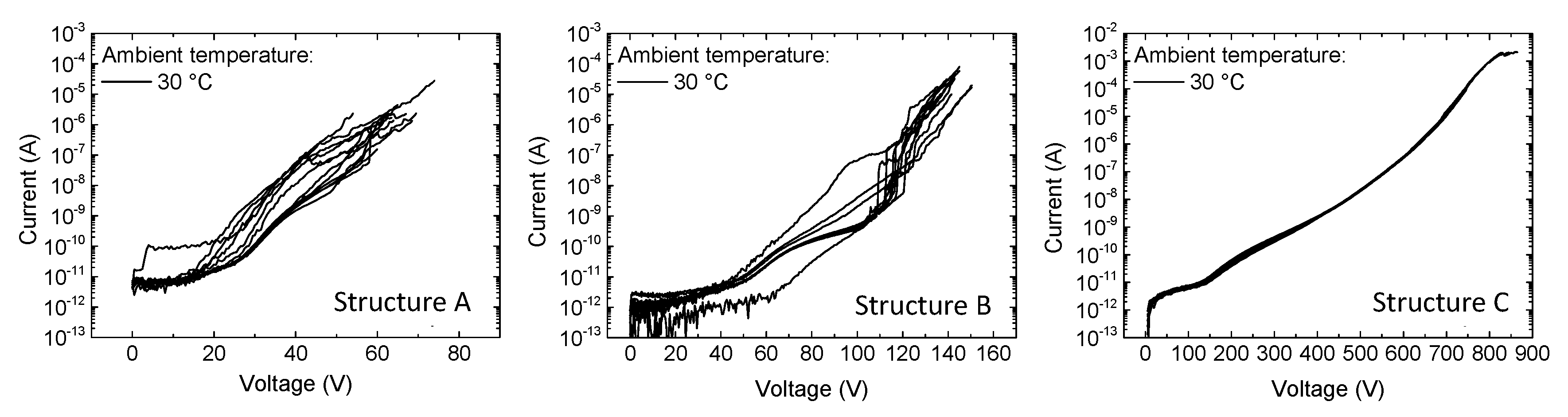
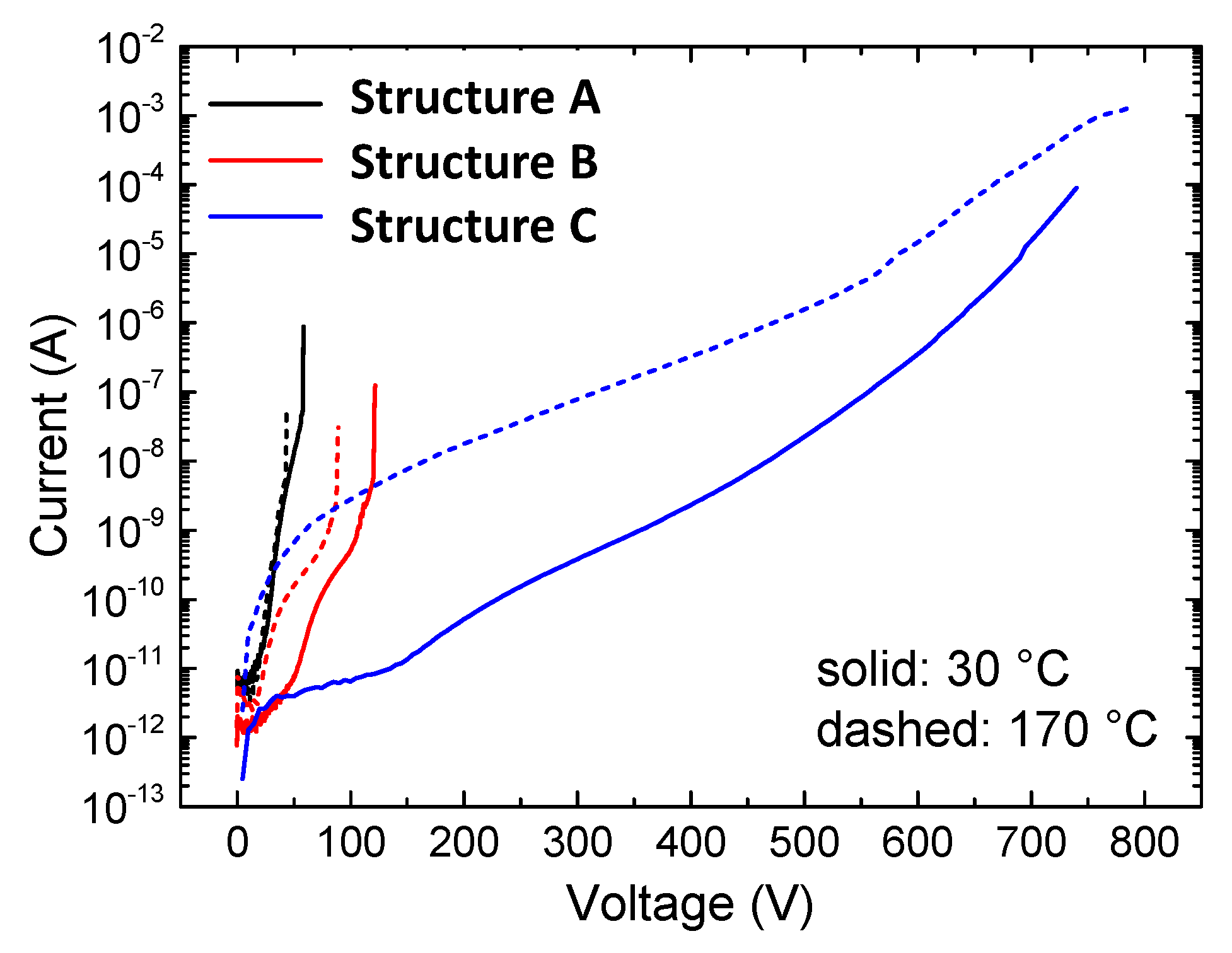
3.2. Vertical Leakage
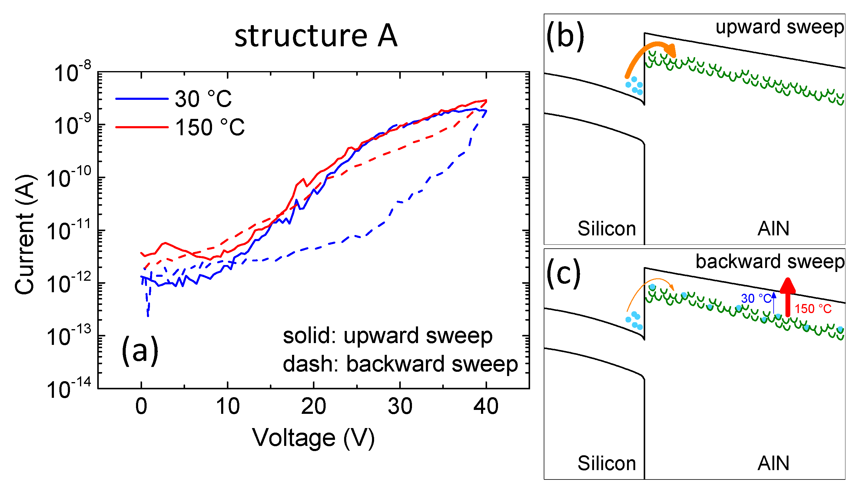
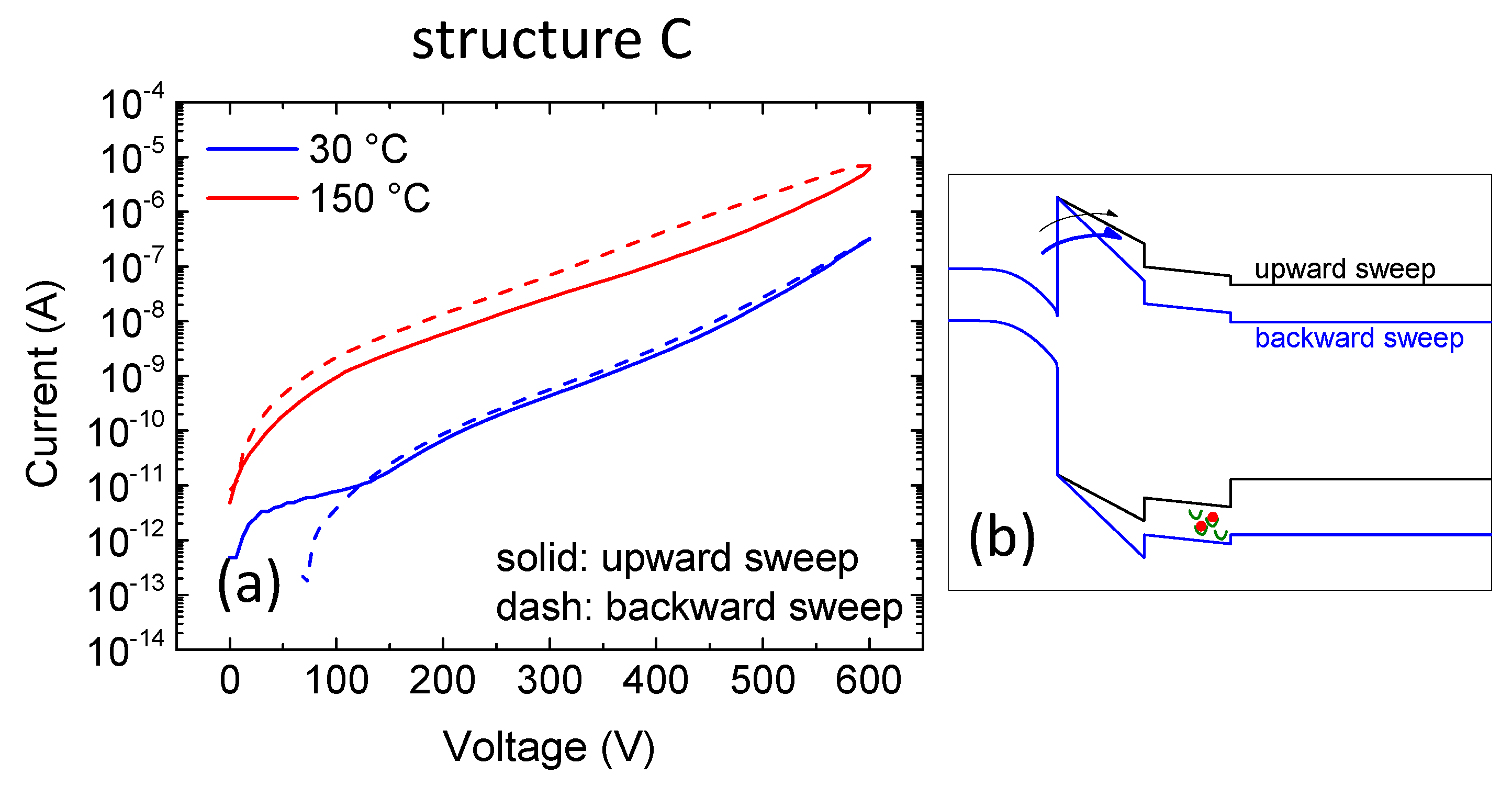
3.3. Charge Trapping
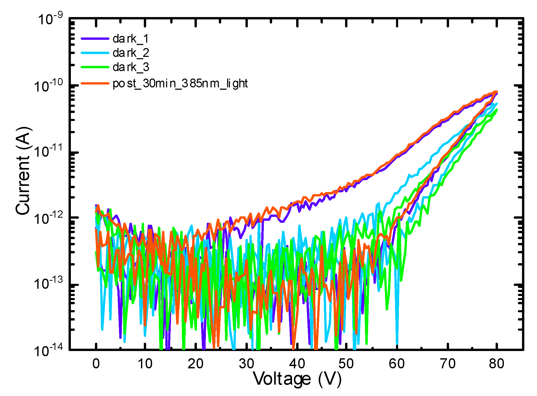
3.4. The Effect of UV Light Irradiation on Current–Voltage Charactrization
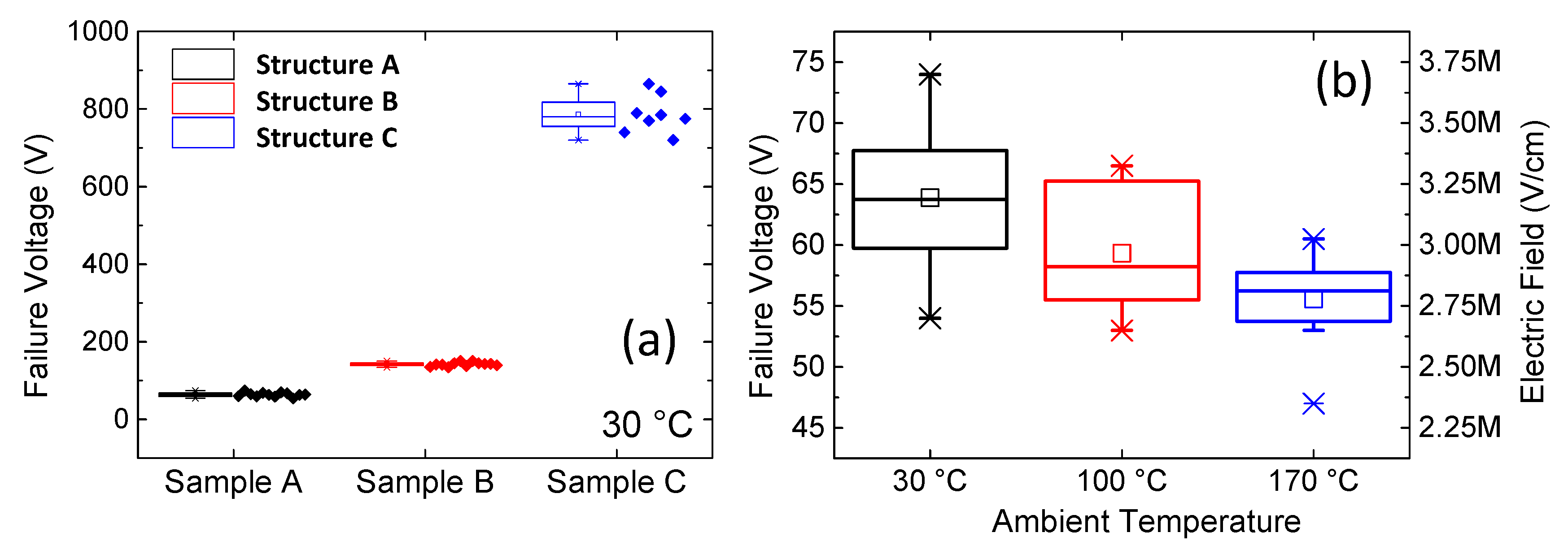
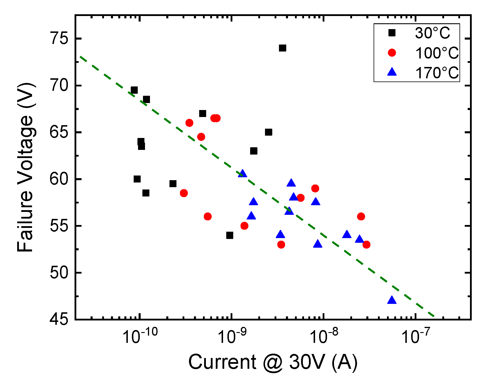
3.5. Vertical Breakdown
4. Conclusions
Author Contributions
Funding
Conflicts of Interest
References
- Amano, H.; Baines, Y.; Beam, E.; Borga, M.; Bouchet, T.; Chalker, P.R.; Charles, M.; Chen, K.J.; Chowdhury, N.; Chu, R.; et al. The 2018 GaN power electronics roadmap. J. Phys. D Appl. Phys. 2018, 51, 163001. [Google Scholar] [CrossRef]
- Kaminski, N.; Hilt, O. SiC and GaN devices—Wide bandgap is not all the same. IET Circuits Devices Syst. 2014, 8, 227–236. [Google Scholar] [CrossRef]
- Meneghini, M.; Meneghesso, G.; Zanoni, E. Power GaN Devices; Springer: Cham, Switzerland, 2017. [Google Scholar]
- Zhou, C.; Jiang, Q.; Huang, S.; Chen, K.J. Vertical leakage/breakdown mechanisms in AlGaN/GaN-on-Si structures. IEEE Electron Device Lett. 2012, 33, 1132–1134. [Google Scholar] [CrossRef]
- Uren, M.J.; Karboyan, S.; Chatterjee, I.; Pooth, A.; Moens, P.; Banerjee, A.; Kuball, M. “Leaky Dielectric” Model for the Suppression of Dynamic Ron in Carbon-Doped AlGaN/GaN HEMTs. IEEE Trans. Electron Devices 2017, 64, 2826–2834. [Google Scholar] [CrossRef]
- Moens, P.; Banerjee, A.; Uren, M.J.; Meneghini, M.; Karboyan, S.; Chatterjee, I.; Vanmeerbeek, P.; Cäsar, M.; Liu, C.; Salih, A.; et al. Impact of buffer leakage on intrinsic reliability of 650V AlGaN/GaN HEMTs. In 2015 IEEE International Electron Devices Meeting (IEDM); IEEE: Piscataway, NJ, USA, 2015. [Google Scholar] [CrossRef]
- Umeda, H.; Suzuki, A.; Anda, Y.; Ishida, M.; Ueda, T.; Tanaka, T.; Ueda, D. Blocking-voltage boosting technology for GaN transistors by widening depletion layer in Si substrates. In 2010 International Electron Devices Meeting; IEEE: Piscataway, NJ, USA, 2010. [Google Scholar] [CrossRef]
- Borga, M.; Meneghini, M.; Benazzi, D.; Canato, E.; Püsche, R.; Derluyn, J.; Abid, I.; Medjdoub, F.; Meneghsso, G.; Zanoni, E. Buffer breakdown in GaN-on-Si HEMTs: A comprehensive study based on a sequential growth experiment. Microelectron. Reliab. 2019, 100, 113461. [Google Scholar] [CrossRef]
- Besendörfer, S.; Meissner, E.; Tajalli, A.; Meneghini, M.; Freitas, J.A., Jr.; Derluyn, J.; Medjdoub, F.; Meneghesso, G.; Friedrich, J.; Erlbacher, T. Vertical breakdown of GaN on Si due to V-pits. J. Appl. Phys. 2020, 127, 015701. [Google Scholar] [CrossRef]
- Yacoub, H.; Fahle, D.; Finken, M.; Hahn, H.; Blumberg, C.; Prost, W.; Kalisch, H.; Herken, M.; Vescan, A. The effect of the inversion channel at the AlN/Si interface on the vertical breakdown characteristics of GaN-based devices. Semicond. Sci. Technol. 2014, 29, 115012. [Google Scholar] [CrossRef]
- Meneghini, M.; Tajalli, A.; Moens, P.; Banerjee, A.; Zanoni, E.; Meneghesso, G. Trapping phenomena and degradation mechanisms in GaN-based power HEMTs. Mater. Sci. Semicond. Process. 2017, 78, 118–126. [Google Scholar] [CrossRef]
- Meneghini, M.; Tajalli, A.; Moens, P.; Banerjee, A.; Stockman, A.; Tack, M.; Gerardin, S.; Bagatin, M.; Paccagnella, A.; Zanoni, E.; et al. Total suppression of dynamic-ron in AlGaN/GaN-HEMTs through proton irradiation. In 2017 IEEE International Electron Devices Meeting (IEDM); IEEE: Piscataway, NJ, USA, 2017; pp. 33.5.1–33.5.4. [Google Scholar] [CrossRef]
- Stockman, A.; Uren, M.; Tajalli, A.; Meneghini, M.; Bakeroot, B.; Moens, P. Temperature dependent substrate trapping in AlGaN/GaN power devices and the impact on dynamic ron. In 2017 47th European Solid-State Device Research Conference (ESSDERC); IEEE: Piscataway, NJ, USA, 2017; pp. 130–133. [Google Scholar] [CrossRef]
- Guo, Q.; Yoshida, A. Temperature Dependence of Band Gap Change in InN and AlN. Jpn. J. Appl. Phys. 1994, 33, 2453–2456. [Google Scholar] [CrossRef]
- Hudgins, J.L.; Simin, G.S.; Santi, E.; Khan, M.A. An assessment of wide bandgap semiconductors for power devices. IEEE Trans. Power Electron. 2003, 18, 907–914. [Google Scholar] [CrossRef]


© 2020 by the authors. Licensee MDPI, Basel, Switzerland. This article is an open access article distributed under the terms and conditions of the Creative Commons Attribution (CC BY) license (http://creativecommons.org/licenses/by/4.0/).
Share and Cite
Tajalli, A.; Borga, M.; Meneghini, M.; De Santi, C.; Benazzi, D.; Besendörfer, S.; Püsche, R.; Derluyn, J.; Degroote, S.; Germain, M.; et al. Vertical Leakage in GaN-on-Si Stacks Investigated by a Buffer Decomposition Experiment. Micromachines 2020, 11, 101. https://doi.org/10.3390/mi11010101
Tajalli A, Borga M, Meneghini M, De Santi C, Benazzi D, Besendörfer S, Püsche R, Derluyn J, Degroote S, Germain M, et al. Vertical Leakage in GaN-on-Si Stacks Investigated by a Buffer Decomposition Experiment. Micromachines. 2020; 11(1):101. https://doi.org/10.3390/mi11010101
Chicago/Turabian StyleTajalli, Alaleh, Matteo Borga, Matteo Meneghini, Carlo De Santi, Davide Benazzi, Sven Besendörfer, Roland Püsche, Joff Derluyn, Stefan Degroote, Marianne Germain, and et al. 2020. "Vertical Leakage in GaN-on-Si Stacks Investigated by a Buffer Decomposition Experiment" Micromachines 11, no. 1: 101. https://doi.org/10.3390/mi11010101
APA StyleTajalli, A., Borga, M., Meneghini, M., De Santi, C., Benazzi, D., Besendörfer, S., Püsche, R., Derluyn, J., Degroote, S., Germain, M., Kabouche, R., Abid, I., Meissner, E., Zanoni, E., Medjdoub, F., & Meneghesso, G. (2020). Vertical Leakage in GaN-on-Si Stacks Investigated by a Buffer Decomposition Experiment. Micromachines, 11(1), 101. https://doi.org/10.3390/mi11010101