Investigation of Intra-Nitride Charge Migration Suppression in SONOS Flash Memory


Abstract
:1. Introduction
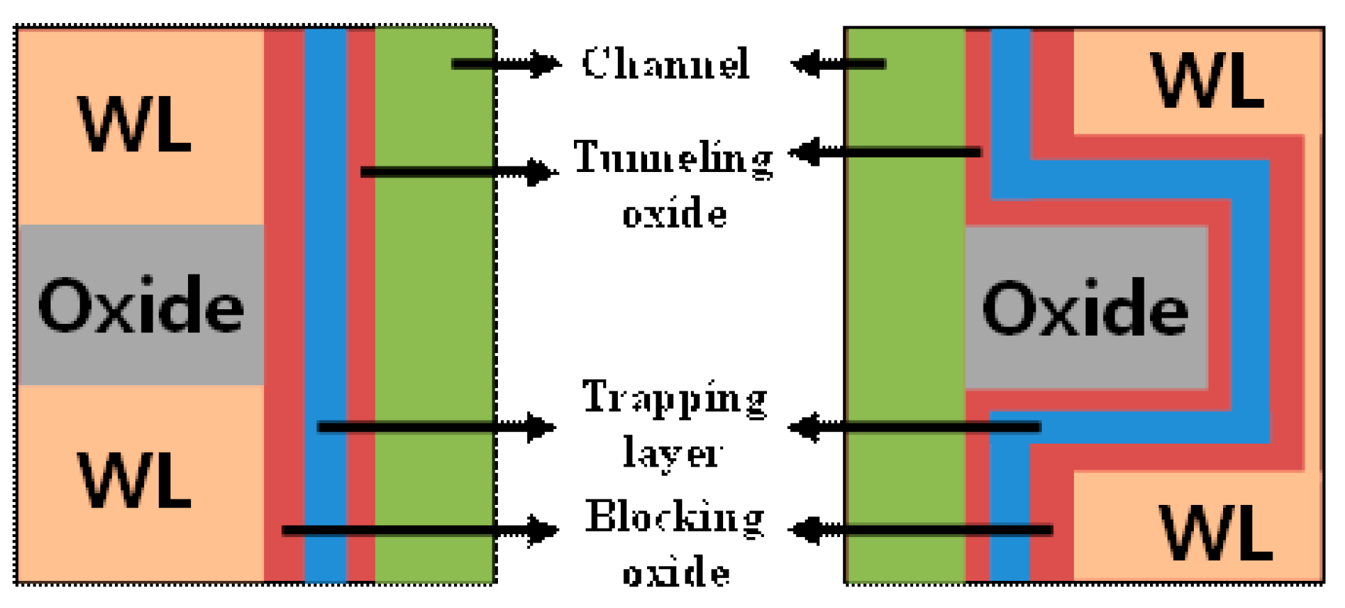
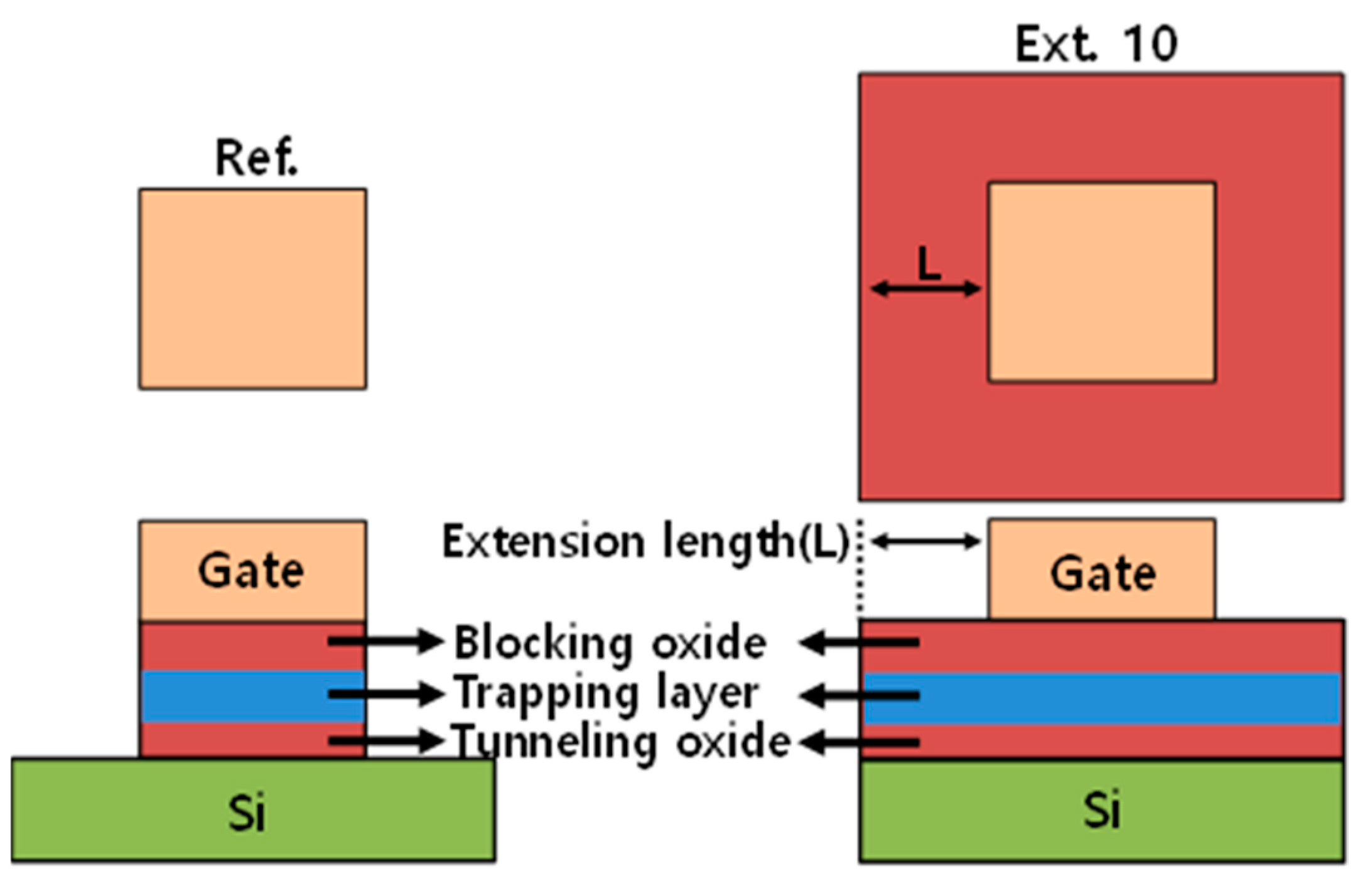
2. Experiments
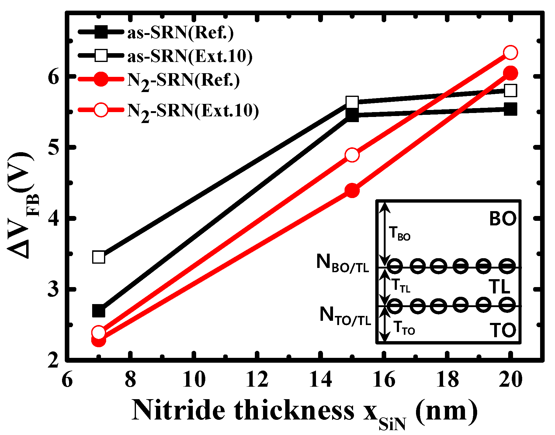
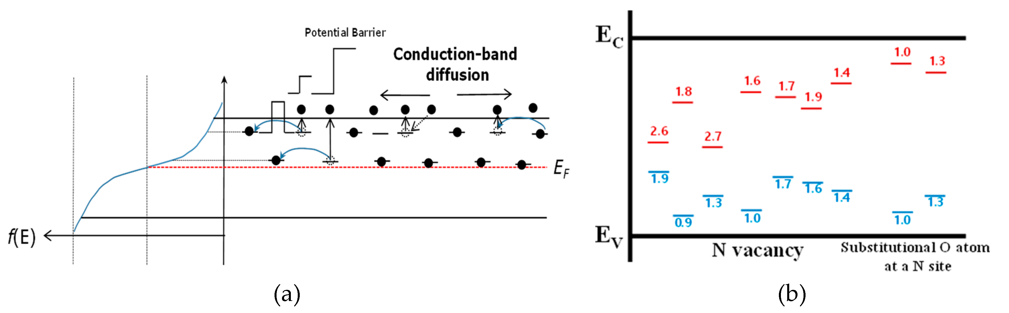
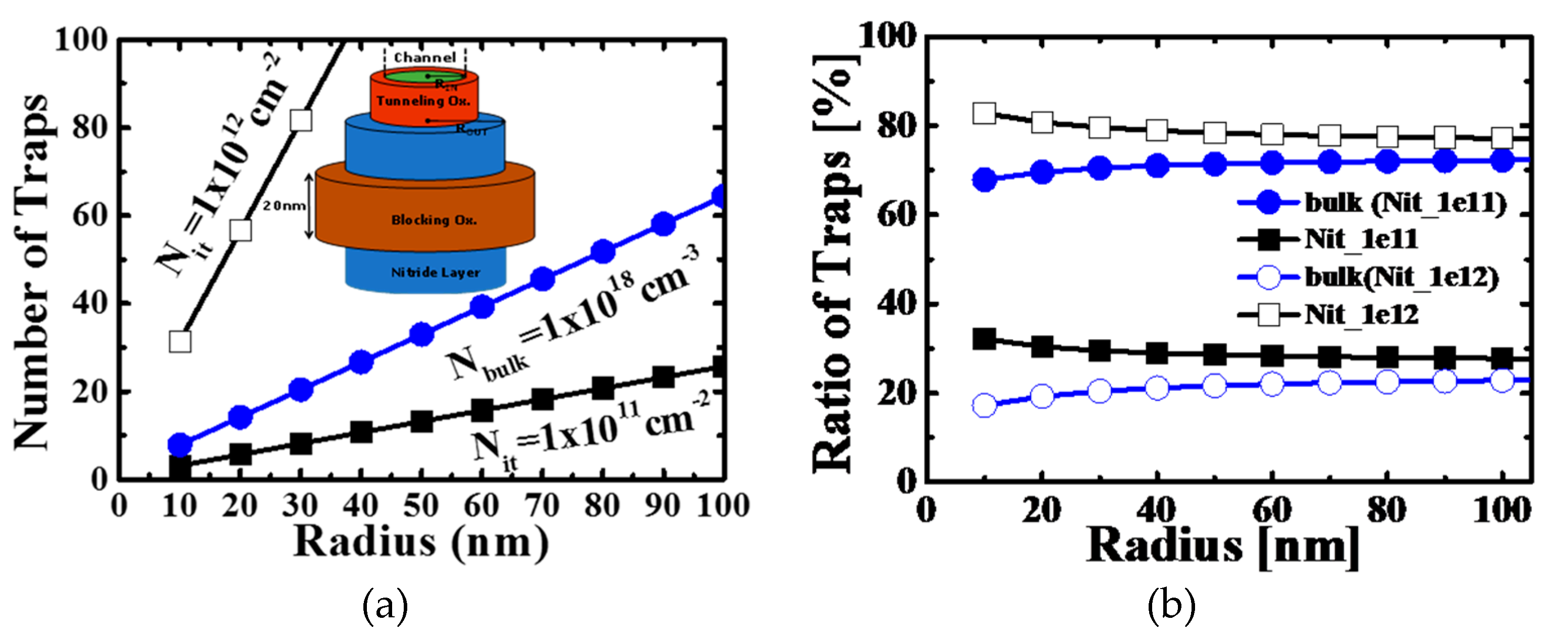
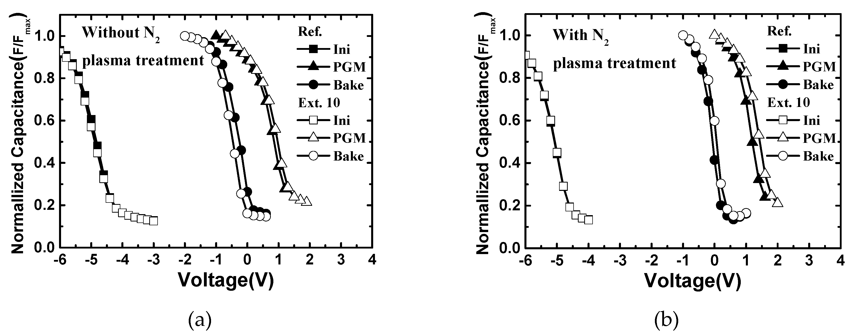
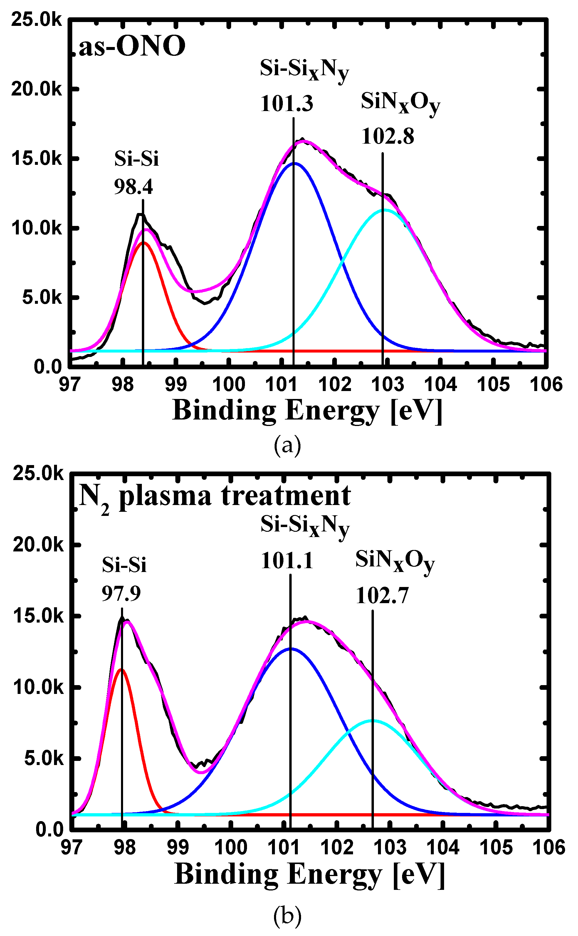
3. Results and Discussion
4. Conclusions
Author Contributions
Funding
Acknowledgments
Conflicts of Interest
References
- Choi, J.; Seol, K.S. 3D approaches for non-volatile memory. In 2011 Symposium on VLSI Technology-Digest of Technical Papers; IEEE: Piscataway, NJ, USA, 2011; pp. 178–179. [Google Scholar]
- Jung, S.-M.; Jang, J.; Cho, W.; Cho, H.; Jeong, J.; Chang, Y.; Kim, J.; Rah, Y.; Son, Y.; Park, J.; et al. Three dimensionally stacked NAND flash memory technology using stacking single crystal Si layers on ILD and TANOS structure for beyond 30nm node. In 2006 International Electron Devices Meeting; IEEE: Piscataway, NJ, USA, 2006; pp. 1–4. [Google Scholar]
- Cho, M.K.; Kim, D.M. High performance SONOS memory cells free of drain turn-on and over-erase: Compatibility issue with current flash technology. IEEE Electron Device Lett. 2000, 21, 399–401. [Google Scholar]
- Park, Y.-W.; Choi, J.; Kang, C.; Lee, C.; Shin, Y.; Choi, B.; Kim, J.; Jeon, S.; Sel, J.; Park, J.; et al. Highly Manufacturable 32Gb Multi -- Level NAND Flash Memory with 0.0098 μm2 Cell Size using TANOS (Si - Oxide - Al2O3 - TaN) Cell Technology. In 2006 International Electron Devices Meeting; IEEE: Piscataway, NJ, USA, 2006; pp. 1–4. [Google Scholar]
- De Salvo, B.; Geradi, C.; van Schaijk, R.; Lombardo, S.A.; Corso, D.; Plantamura, C.; Serafino, S.; Ammendola, G.; van Duuren, M.; Goarin, P.; et al. Performance and reliability features of advanced nonvolatile memories based on discrete traps (silicon nanocrystals, SONOS). IEEE Trans. Device Mater. Reliab. 2004, 4, 377–389. [Google Scholar] [CrossRef]
- Tanaka, H.; Kido, M.; Yahashi, K.; Oomura, M.; Katsumata, R.; Kito, M.; Fukuzumi, Y.; Sato, M.; Nagata, Y.; Matsuoka, Y.; et al. Bit Cost Scalable Technology with Punch and Plug Process for Ultra High Density Flash Memory. In 2007 IEEE Symposium on VLSI Technology; IEEE: Piscataway, NJ, USA, 2007; pp. 14–15. [Google Scholar]
- Katsumata, R.; Kito, M.; Fukuzumi, Y.; Kido, M.; Tanaka, H.; Koromi, Y.; Ishiduki, M.; Matsunami, J.; Fujiwara, T.; Nagata, Y.; et al. Pipe-shaped BiCS flash memory with 16 stacked layers and multi-level-cell operation for ultra-high density storage devices. In 2009 Symposium on VLSI Technology; IEEE: Piscataway, NJ, USA, 2009; pp. 136–137. [Google Scholar]
- Jang, J.-H.; Kim, H.-S.; Cho, W.; Cho, H.; Kim, J.; Shim, S.I.; Jeong, J.H.; Son, B.-K.; Kim, D.W.; Shim, J.-J.; et al. Vertical Cell Array using TCAT (Terabit Cell Array Transistor) Technology for Ultra High Density NAND Flash Memory. In 2009 Symposium on VLSI Technology; IEEE: Piscataway, NJ, USA, 2009; pp. 192–193. [Google Scholar]
- Kim, W.-J.; Choi, S.; Sung, J.; Lee, T.; Park, C.; Ko, H.; Jung, J.; Yoo, I.; Park, Y. “Multi-layered Vertical Gate NAND Flash overcoming stacking limit for terabit density storage. In 2009 Symposium on VLSI Technology; IEEE: Piscataway, NJ, USA, 2009; pp. 188–189. [Google Scholar]
- Choi, E.S.; Park, S.K. Device considerations for high density and highly reliable 3D NAND flash cell in near future. In 2012 International Electron Devices Meeting; IEEE: Piscataway, NJ, USA, 2012; pp. 9.4.1–9.4.4. [Google Scholar]
- Maconi, A.; Arreghini, A.; Compagnoni, C.M.; Spinelli, A.S.; van Houdt, J.; Lacaita, A.L. Impact of lateral charge migration on the retention performance of planar and 3D SONOS devices. In 2011 Proceedings of the European Solid-State Device Research Conference (ESSDERC); IEEE: Piscataway, NJ, USA, 2011; pp. 195–198. [Google Scholar]
- Kang, C.-S.; Choi, J.; Sim, J.; Lee, C.; Shin, Y.; Park, J.; Sel, J.; Jeon, S.; Park, Y.; Kim, K.-N. Effects of lateral charge spreading on the reliability of TANOS (TaN/AlO/SiN/Oxide/Si) NAND flash memory. In 2007 IEEE International Reliability Physics Symposium Proceedings. 45th Annual; IEEE: Piscataway, NJ, USA, 2007; pp. 167–170. [Google Scholar]
- Maconi, A.; Arreghini, A.; Compagnoni, C.M.; Spinelli, A.S.; van Houdt, J.; Lacaita, A.L. Comprehensive investigation of the impact of lateral charge migration on retention performance of planar and 3D SONOS devices. Solid-State Electron. 2012, 74, 64–70. [Google Scholar] [CrossRef]
- Liu, L.; Arreghini, A.; Pan, L.; van Houdt, J. Comprehensive understanding of charge lateral migration in 3D SONOS memories. Solid-State Electron. 2016, 116, 95–99. [Google Scholar] [CrossRef]
- Morokov, Y.N.; Novikov, Y.N.; Gritsenko, V.A.; Wong, H. Two-fold coordinated nitrogen atom: an electron trap in MOS devices with silicon oxynitride as the gate dielectric. Microelectron. Eng. 1999, 48, 175–178. [Google Scholar] [CrossRef]
- Wong, H.; Gritsenko, V.A. Defects in silicon oxynitride gate dielectric films. Microelectron. Reliab. 2002, 42, 597–605. [Google Scholar] [CrossRef]
- Perera, R.; Ikeda, A.; Hattori, R.; Kuroki, Y. Effects of post annealing on removal of defect states in silicon oxynitride films grown by oxidation of silicon substrates nitrided in inductively coupled nitrogen plasma. Thin Solid Films 2003, 423, 212–217. [Google Scholar] [CrossRef]
- Ishida, T.; Okuyama, Y.; Yamada, R. Characterization of charge traps in metal-oxide-nitride-oxide-semiconductor (MONOS) structures for embedded flash memories. In 2006 IEEE International Reliability Physics Symposium Proceedings; IEEE: Piscataway, NJ, USA, 2006; pp. 516–522. [Google Scholar]


| Sample | NBO/TL (cm−2) | NTO/TL (cm−2) | Charge Loss [%] |
|---|---|---|---|
| Ref. | 2.53 × 10¹² | 8.91 × 10¹¹ | 18.6 |
| Ext.10 | 4.36 × 10¹² | 7.32 × 10¹¹ | 25.7 |
| N2 plasma treated Ref. | 4.35 × 10¹¹ | 1.11 × 10¹² | 17.3 |
| N2 plasma treated Ext.10 | 5.21 × 10¹¹ | 1.18 × 10¹² | 20.5 |
© 2019 by the authors. Licensee MDPI, Basel, Switzerland. This article is an open access article distributed under the terms and conditions of the Creative Commons Attribution (CC BY) license (http://creativecommons.org/licenses/by/4.0/).
Share and Cite
Yang, S.-D.; Jung, J.-K.; Lim, J.-G.; Park, S.-g.; Lee, H.-D.; Lee, G.-W. Investigation of Intra-Nitride Charge Migration Suppression in SONOS Flash Memory. Micromachines 2019, 10, 356. https://doi.org/10.3390/mi10060356
Yang S-D, Jung J-K, Lim J-G, Park S-g, Lee H-D, Lee G-W. Investigation of Intra-Nitride Charge Migration Suppression in SONOS Flash Memory. Micromachines. 2019; 10(6):356. https://doi.org/10.3390/mi10060356
Chicago/Turabian StyleYang, Seung-Dong, Jun-Kyo Jung, Jae-Gab Lim, Seong-gye Park, Hi-Deok Lee, and Ga-Won Lee. 2019. "Investigation of Intra-Nitride Charge Migration Suppression in SONOS Flash Memory" Micromachines 10, no. 6: 356. https://doi.org/10.3390/mi10060356
APA StyleYang, S.-D., Jung, J.-K., Lim, J.-G., Park, S.-g., Lee, H.-D., & Lee, G.-W. (2019). Investigation of Intra-Nitride Charge Migration Suppression in SONOS Flash Memory. Micromachines, 10(6), 356. https://doi.org/10.3390/mi10060356