A Novel GaN Metal-Insulator-Semiconductor High Electron Mobility Transistor Featuring Vertical Gate Structure


Abstract
1. Introduction
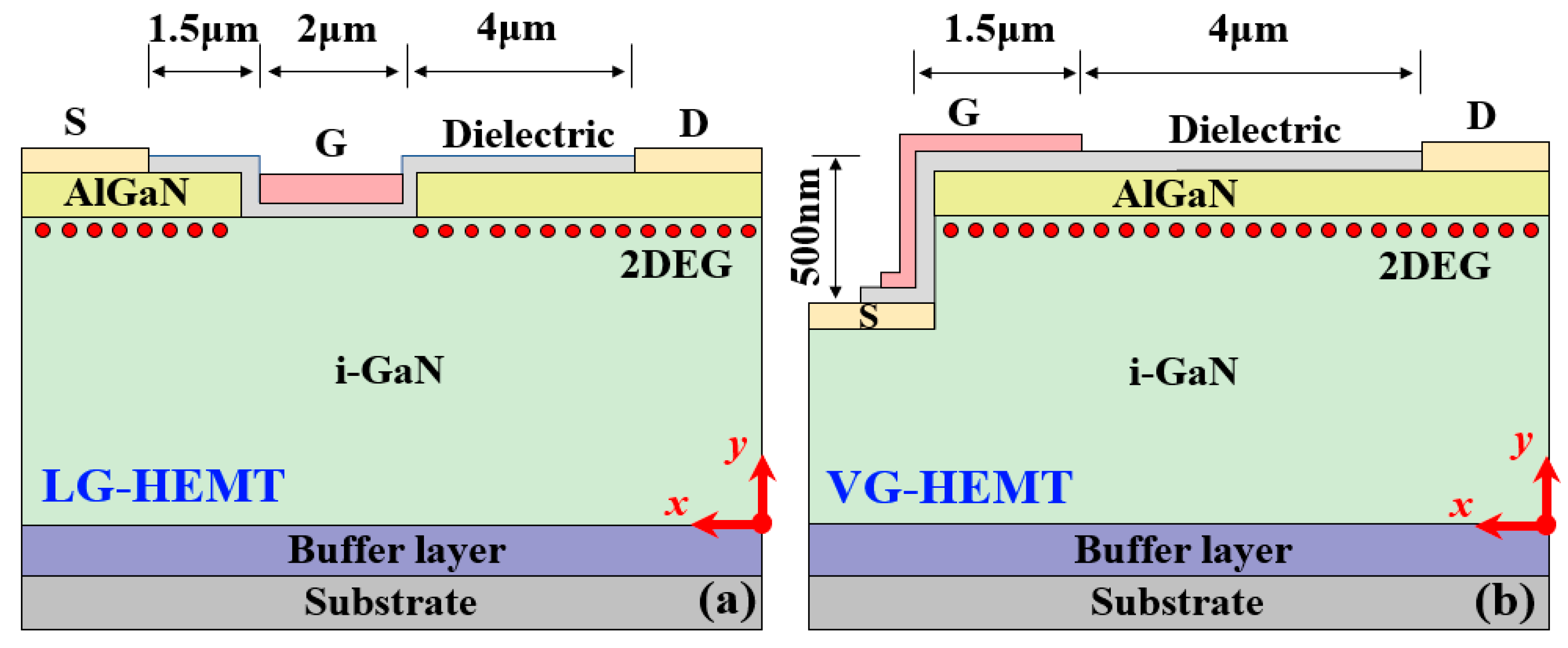
2. The Proposed Device and Physical Principle
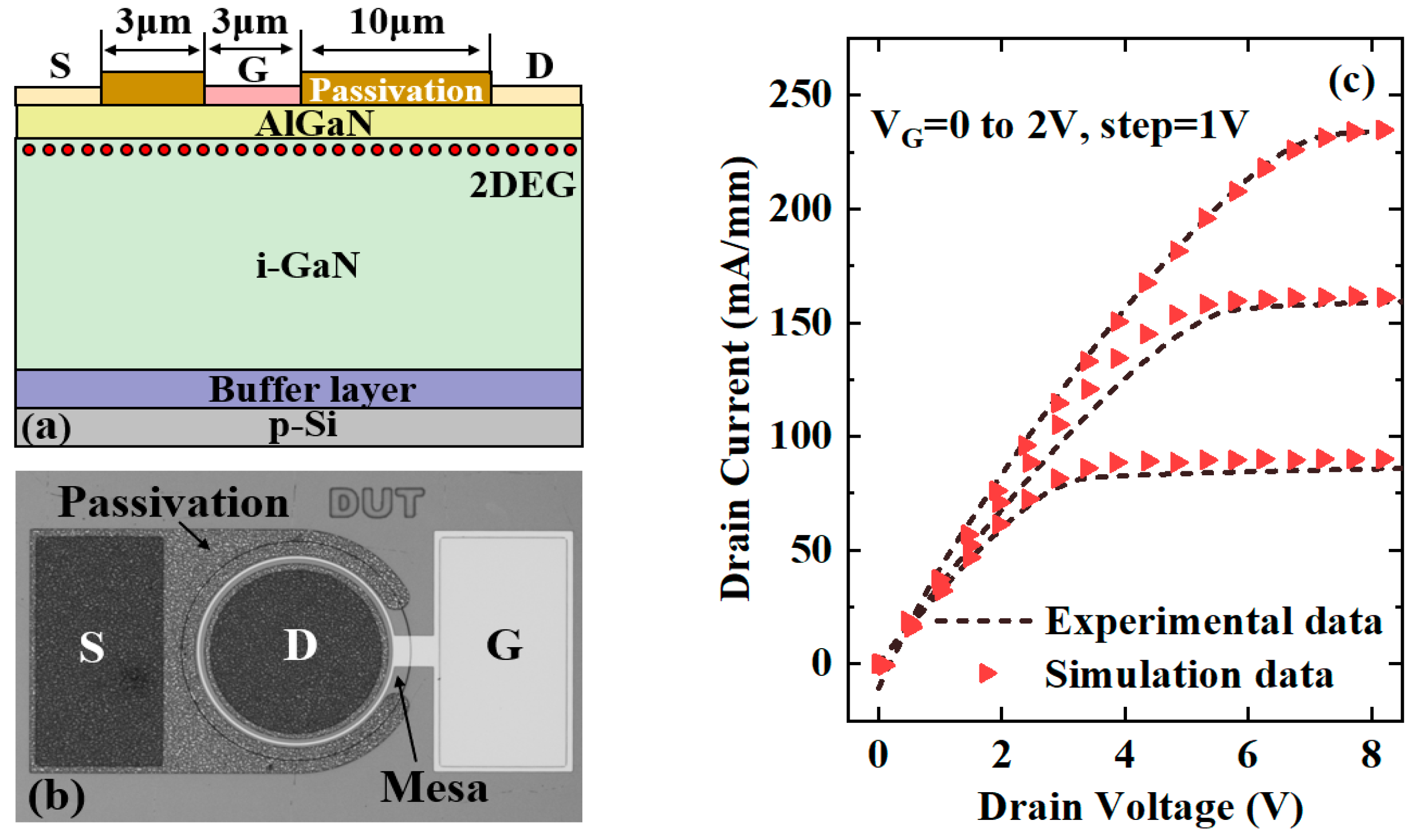
3. Fabrication Work and Parameter Calibration for TCAD simulation
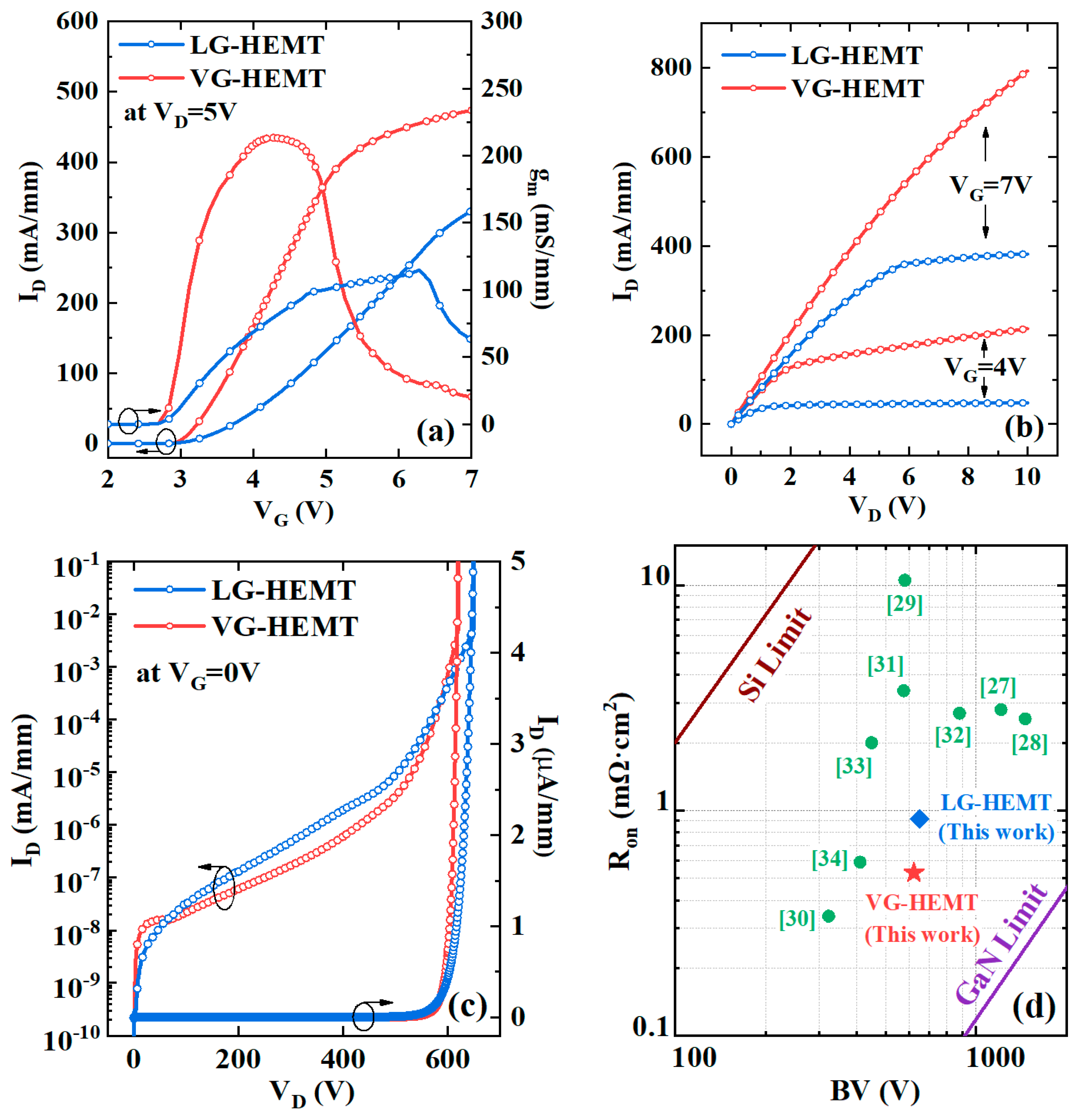
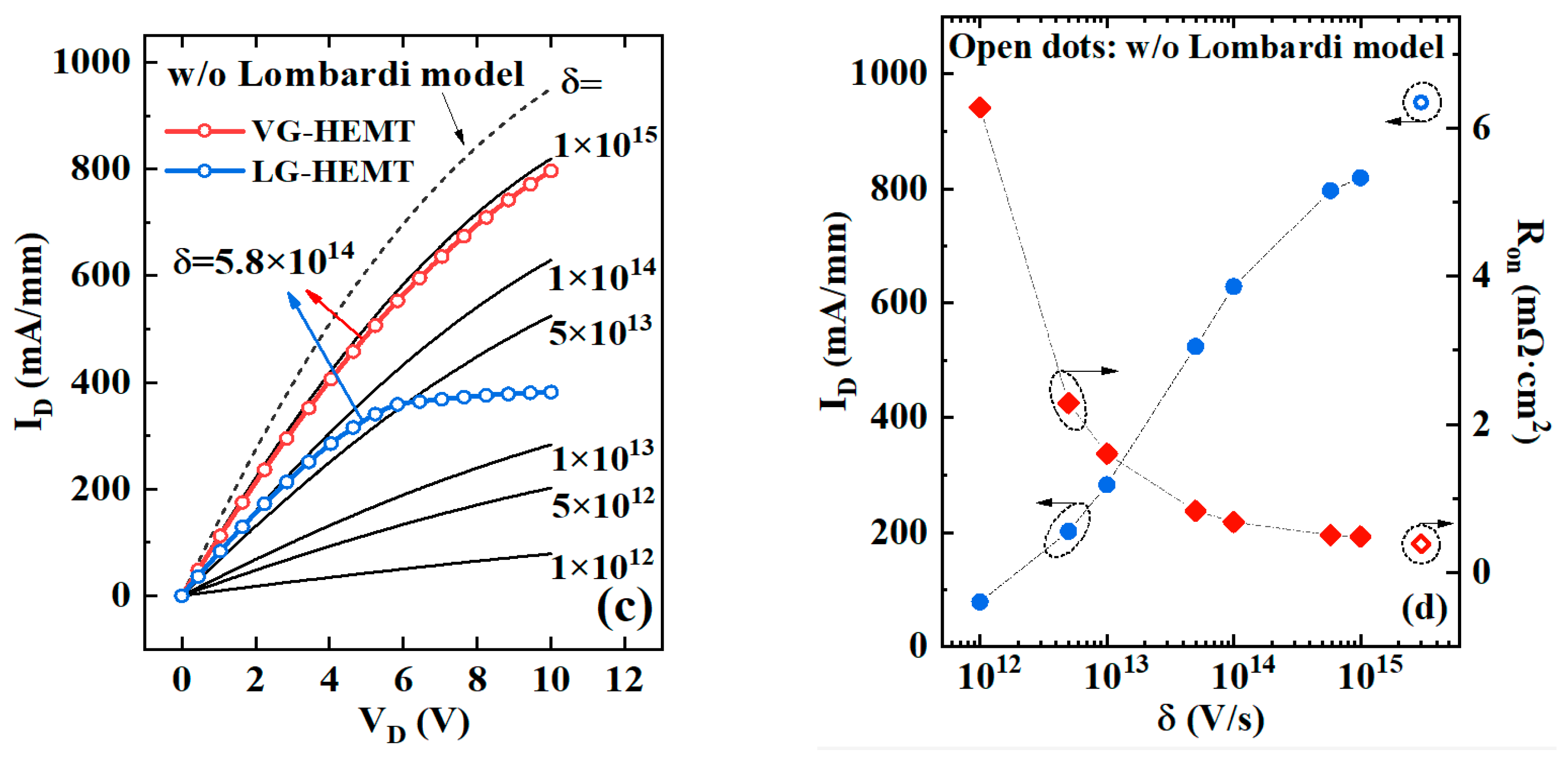
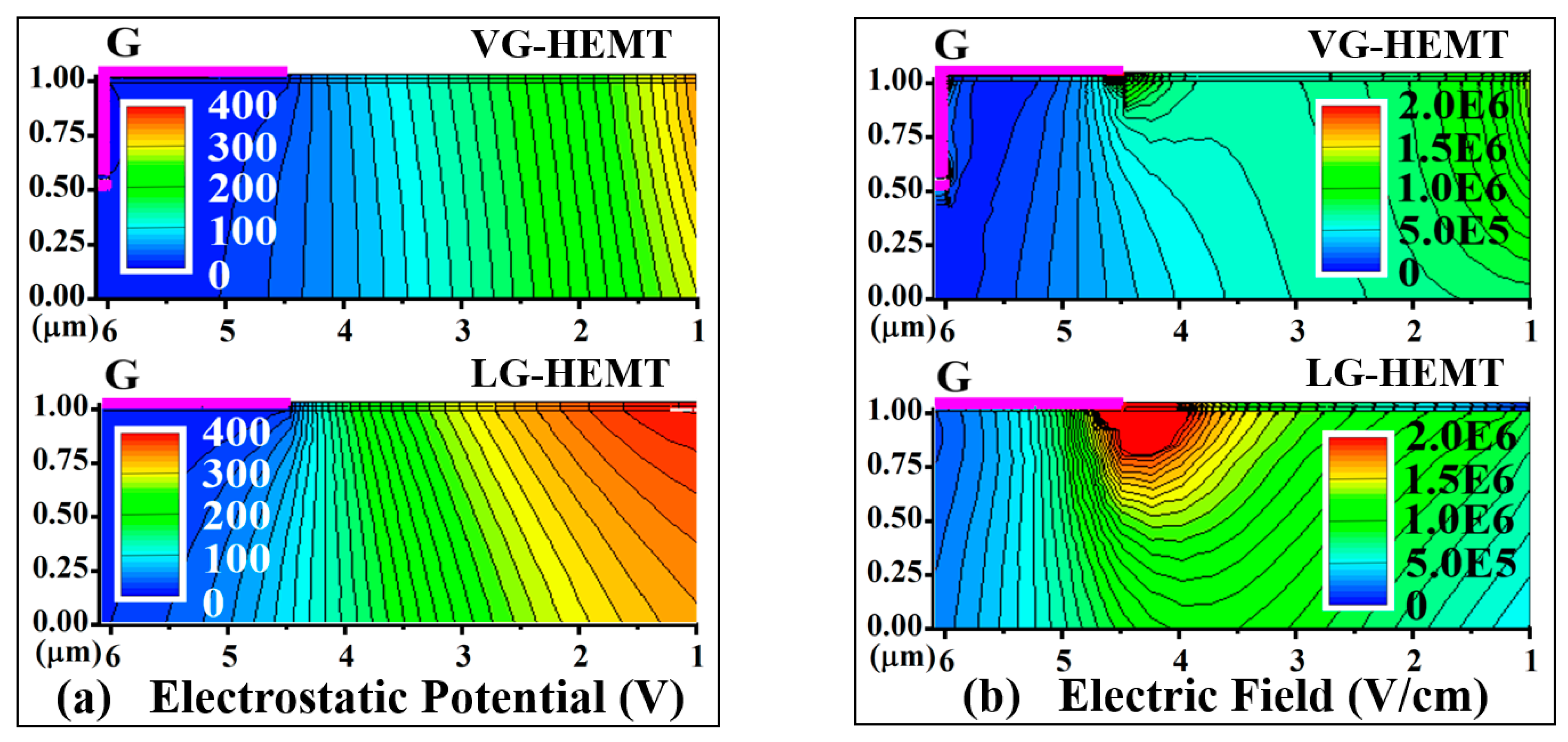
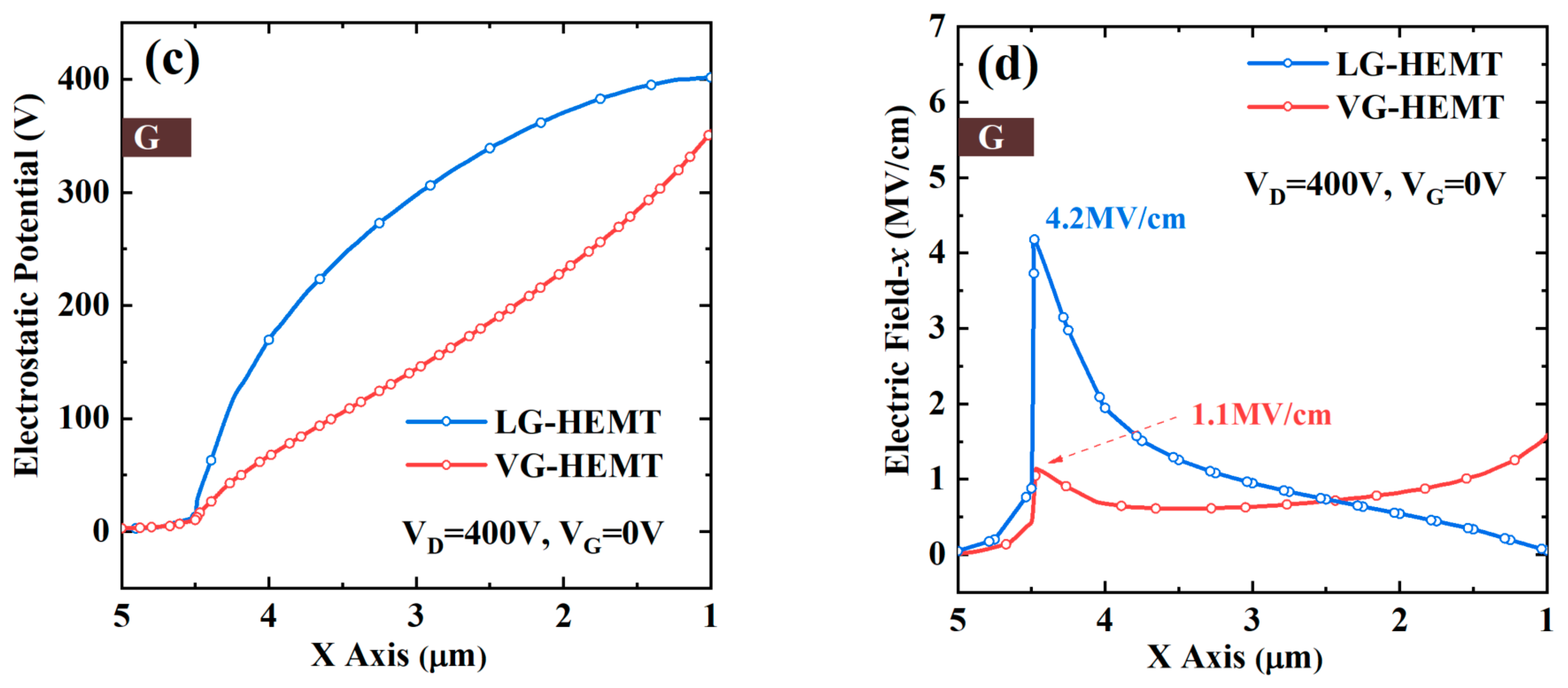
4. Results and Discussions
5. Conclusion
Author Contributions
Funding
Conflicts of Interest
References
- Fukushima, H.; Usami, S.; Ogura, M.; Ando, Y.; Tanaka, A.; Deki, M.; Kushimoto, M.; Nitta, S.; Honda, Y.; Amano, H. Vertical GaN pn diode with deeply etched mesa and capability of avalanche breakdown. Appl. Phys. Express 2019, 12. [Google Scholar] [CrossRef]
- Ando, Y.; Kaneki, S.; Hashizume, T. Improved operation stability of Al2O3/AlGaN/GaN MOS high-electron-mobility transistors grown on GaN substrates. Appl. Phys. Express 2019, 12, 024002. [Google Scholar] [CrossRef]
- Huang, H.; Liang, Y.C.; Samudra, G.S.; Chang, T.F.; Huang, C.F. Effects of gate field plates on the surface state related current collapse in AlGaN/GaN HEMTs. IEEE Trans. Power Electron. 2013, 29, 2164–2173. [Google Scholar] [CrossRef]
- Chen, K.J.; Häberlen, O.; Lidow, A.; lin Tsai, C.; Ueda, T.; Uemoto, Y.; Wu, Y. GaN-on-Si power technology: Devices and applications. IEEE Trans. Electron Devices 2017, 64, 779–795. [Google Scholar] [CrossRef]
- Huang, H.; Sun, Z.; Cao, Y.; Li, F.; Zhang, F.; Wen, Z.; Zhang, Z.; Liang, Y.C.; Hu, L. Investigation of surface traps-induced current collapse phenomenon in AlGaN/GaN high electron mobility transistors with schottky gate structures. J. Phys. D Appl. Phys. 2018, 51, 345102. [Google Scholar] [CrossRef]
- Wei, J.; Lei, J.; Tang, X.; Li, B.; Liu, S.; Chen, K.J. Channel-to-channel coupling in normally-off GaN double-channel MOS-HEMT. IEEE Electron Device Lett. 2017, 39, 59–62. [Google Scholar] [CrossRef]
- Rossetto, I.; Meneghini, M.; De Santi, C.; Pandey, S.; Gajda, M.; Hurkx, G.M.; Croon, J.; Šonský, J.; Meneghesso, G. 2DEG retraction and potential distribution of GaN–on–Si HEMTs investigated through a floating gate terminal. IEEE Trans. Electron Devices 2018, 65, 1303–1307. [Google Scholar] [CrossRef]
- Wang, H.; Wei, J.; Xie, R.; Liu, C.; Tang, G.; Chen, K.J. Maximizing the performance of 650-V p-GaN gate HEMTs: Dynamic RON characterization and circuit design considerations. IEEE Trans. Power Electron. 2016, 32, 5539–5549. [Google Scholar] [CrossRef]
- Sun, R.; Liang, Y.C.; Yeo, Y.C.; Zhao, C. Au-Free AlGaN/GaN MIS-HEMTs With Embedded Current Sensing Structure for Power Switching Applications. IEEE Trans. Electron Devices 2017, 64, 3515–3518. [Google Scholar] [CrossRef]
- Shen, F.; Hao, R.; Song, L.; Chen, F.; Yu, G.; Zhang, X.; Fan, Y.; Lin, F.; Cai, Y.; Zhang, B. Enhancement mode AlGaN/GaN HEMTs by fluorine ion thermal diffusion with high V th stability. Appl. Phys. Express 2019, 12, 066501. [Google Scholar] [CrossRef]
- Wu, T.L.; Marcon, D.; You, S.; Posthuma, N.; Bakeroot, B.; Stoffels, S.; Van Hove, M.; Groeseneken, G.; Decoutere, S. Forward bias gate breakdown mechanism in enhancement-mode p-GaN gate AlGaN/GaN high-electron mobility transistors. IEEE Electron Device Lett. 2015, 36, 1001–1003. [Google Scholar] [CrossRef]
- Wang, H.; Wang, J.; Li, M.; Cao, Q.; Yu, M.; He, Y.; Wu, W. 823-mA/mm Drain Current Density and 945-MW/cm 2 Baliga’s Figure-of-Merit Enhancement-Mode GaN MISFETs With a Novel PEALD-AlN/LPCVD-Si 3 N 4 Dual-Gate Dielectric. IEEE Electron Device Lett. 2018, 39, 1888–1891. [Google Scholar] [CrossRef]
- Wang, Y.H.; Liang, Y.C.; Samudra, G.S.; Huang, H.; Huang, B.J.; Huang, S.H.; Chang, T.F.; Huang, C.F.; Kuo, W.H.; Lo, G.Q. 6.5 V high threshold voltage AlGaN/GaN power metal-insulator-semiconductor high electron mobility transistor using multilayer fluorinated gate stack. IEEE Electron Device Lett. 2015, 36, 381–383. [Google Scholar] [CrossRef]
- Huang, H.; Liang, Y.C. Formation of combined partially recessed and multiple fluorinated-dielectric layers gate structures for high threshold voltage GaN-based HEMT power devices. Solid-State Electron. 2015, 114, 148–154. [Google Scholar] [CrossRef]
- Huang, X.; Liu, Z.; Lee, F.C.; Li, Q. Characterization and enhancement of high-voltage cascode GaN devices. IEEE Trans. Electron Devices. 2014, 62, 270–277. [Google Scholar] [CrossRef]
- Ren, J.; Tang, C.W.; Feng, H.; Jiang, H.; Yang, W.; Zhou, X.; Lau, K.M.; Sin, J.K. A Novel 700 V Monolithically Integrated Si-GaN Cascoded Field Effect Transistor. IEEE Electron Device Lett. 2018, 39, 394–396. [Google Scholar] [CrossRef]
- Oka, T.; Nozawa, T. AlGaN/GaN recessed MIS-gate HFET with high-threshold-voltage normally-off operation for power electronics applications. IEEE Electron Device Lett. 2008, 29, 668–670. [Google Scholar] [CrossRef]
- Li, X.; Hove, M.V.; Zhao, M.; Geens, K.; Lempinen, V.P.; Sormunen, J.; Groeseneken, G.; Decoutere, S. 200 V Enhancement-Mode p-GaN HEMTs Fabricated on 200 mm GaN-on-SOI with Trench Isolation for Monolithic Integration. IEEE Electron Device Lett. 2017, 38, 918–921. [Google Scholar] [CrossRef]
- Ma, J.; Matioli, E. High performance tri-gate GaN power MOSHEMTs on silicon substrate. IEEE Electron Device Lett. 2017, 38, 367–370. [Google Scholar] [CrossRef]
- Zhang, Y.; Sun, M.; Piedra, D.; Hu, J.; Liu, Z.; Lin, Y.; Gao, X.; Shepard, K.; Palacios, T. 1200 V GaN vertical fin power field-effect transistors. In Proceedings of the 2017 IEEE International Electron Devices Meeting (IEDM), San Francisco, CA, USA, 2–6 December 2017; pp. 9.2.1–9.2.4. [Google Scholar]
- Nishimura, T.; Kasai, T.; Mishima, T.; Kuriyama, K.; Nakamura, T. Reduction in contact resistance and structural evaluation of Al/Ti electrodes on Si-implanted GaN. NUCL INSTRUM METHODS PHYS RES B 2019, 450, 244–247. [Google Scholar] [CrossRef]
- Arora, N.D.; Hauser, J.R.; Roulston, D.J. Electron and hole mobilities in silicon as a function of concentration and temperature. IEEE Trans. Electron Devices 1982, 29, 292–295. [Google Scholar] [CrossRef]
- Barnes, J.J.; Lomax, R.J.; Haddad, G.I. Finite-element simulation of GaAs MESFET’s with lateral doping profiles and submicron gates. IEEE Trans. Electron Devices 1976, 23, 1042–1048. [Google Scholar] [CrossRef]
- Lombardi, C.; Manzini, S.; Saporito, A.; Vanzi, M. A physically based mobility model for numerical simulation of nonplanar devices. IEEE Trans. Comput. Aided Des. Integr. Circuits Syst. 1988, 7, 1164–1171. [Google Scholar] [CrossRef]
- Zhang, Y.; Sun, M.; Joglekar, S.J.; Fujishima, T.; Palacios, T. Threshold voltage control by gate oxide thickness in fluorinated GaN metal-oxide-semiconductor high-electron-mobility transistors. Appl. Phys. Lett. 2013, 103, 033524. [Google Scholar] [CrossRef]
- Hua, M.; Zhang, Z.; Wei, J.; Lei, J.; Tang, G.; Fu, K.; Cai, Y.; Zhang, B.; Chen, K.J. Integration of LPCVD-SiN x gate dielectric with recessed-gate E-mode GaN MIS-FETs: Toward high performance, high stability and long TDDB lifetime. In Proceedings of the 2016 IEEE International Electron Devices Meeting (IEDM), San Francisco, CA, USA, 3–7 December 2016; pp. 10.4.1–10.4.4. [Google Scholar]
- Yang, C.; Luo, X.; Zhang, A.; Deng, S.; Ouyang, D.; Peng, F.; Wei, J.; Zhang, B.; Li, Z. AlGaN/GaN MIS-HEMT with AlN interface protection layer and trench termination structure. IEEE Trans. Electron Devices 2018, 65, 5203–5207. [Google Scholar] [CrossRef]
- Hao, R.; Li, W.; Fu, K.; Yu, G.; Song, L.; Yuan, J.; Li, J.; Deng, X.; Zhang, X.; Zhou, Q.; et al. Breakdown enhancement and current collapse suppression by high-resistivity GaN cap layer in normally-off AlGaN/GaN HEMTs. IEEE Electron Device Lett. 2017, 38, 1567–1570. [Google Scholar] [CrossRef]
- Hu, Q.; Li, S.; Li, T.; Wang, X.; Li, X.; Wu, Y. Channel Engineering of Normally-OFF AlGaN/GaN MOS-HEMTs by Atomic Layer Etching and High-k Dielectric. IEEE Electron Device Lett. 2018, 39, 1377–1380. [Google Scholar] [CrossRef]
- Huang, H.; Liang, Y.C.; Samudra, G.S.; Ngo, C.L. Au-free normally-off AlGaN/GaN-on-Si MIS-HEMTs using combined partially recessed and fluorinated trap-charge gate structures. IEEE Electron Device Lett. 2014, 35, 569–571. [Google Scholar] [CrossRef]
- Lin, S.; Wang, M.; Sang, F.; Tao, M.; Wen, C.P.; Xie, B.; Yu, M.; Wang, J.; Hao, Y.; Wu, W.; et al. A GaN HEMT structure allowing self-terminated, plasma-free etching for high-uniformity, high-mobility enhancement-mode devices. IEEE Electron Device Lett. 2016, 37, 377–380. [Google Scholar] [CrossRef]
- Zhang, Z.; Fu, K.; Deng, X.; Zhang, X.; Fan, Y.; Sun, S.; Song, L.; Xing, Z.; Huang, W.; Yu, G.; et al. Normally Off AlGaN/GaN MIS-high-electron mobility transistors fabricated by using low pressure chemical vapor deposition Si 3 N 4 gate dielectric and standard fluorine ion implantation. IEEE Electron Device Lett. 2015, 36, 1128–1131. [Google Scholar] [CrossRef]
- Zhang, Z.; Li, W.; Fu, K.; Yu, G.; Zhang, X.; Zhao, Y.; Sun, S.; Song, L.; Deng, X.; Xing, Z.; et al. AlGaN/GaN MIS-HEMTs of Very-Low V Hysteresis and Current Collapse With In-Situ Pre-Deposition Plasma Nitridation and LPCVD-Si3N4 Gate Insulator. IEEE Electron Device Lett. 2016, 38, 236–239. [Google Scholar] [CrossRef]
- Xu, Z.; Wang, J.; Liu, J.; Jin, C.; Cai, Y.; Yang, Z.; Wang, M.; Yu, M.; Xie, B.; Wu, W.; et al. Demonstration of normally-off recess-gated AlGaN/GaN MOSFET using GaN cap layer as recess mask. IEEE Electron Device Lett. 2014, 35, 1197–1199. [Google Scholar]
- Sze, S.M.; Ng, K.K. Physics of semiconductor devices, 3rd ed.; John wiley & sons: Hoboken, NJ, USA, 2006; pp. 225–316. [Google Scholar]
- Rodriguez, N.; Roldan, J.B.; Gamiz, F. An electron mobility model for ultra-thin gate-oxide MOSFETs including the contribution of remote scattering mechanisms. Semicond. Sci. Technol. 2007, 22, 348. [Google Scholar] [CrossRef]
- Du, J.; Yan, H.; Yin, C.; Feng, Z.; Dun, S.; Yu, Q. Simulation and characterization of millimeter-wave InAlN/GaN high electron mobility transistors using Lombardi mobility model. J. Appl. Phys. 2014, 115, 164510. [Google Scholar] [CrossRef]


| Physical Parameters | Values |
|---|---|
| Electron effective mass in GaN | 0.22·me |
| Electron affinity | 3.4 eV |
| Relative dielectric constant in GaN | 9.7 |
| Background electron concentration in i-GaN layer | 5.0 × 1015 cm−3 |
| Electron mobility in 2DEG channel | 1500 cm2/(V·s) |
| 2DEG sheet density | 8.0 × 1012 cm−2 |
| Electron saturation velocity in GaN | 1.8 × 107 cm/s |
© 2019 by the authors. Licensee MDPI, Basel, Switzerland. This article is an open access article distributed under the terms and conditions of the Creative Commons Attribution (CC BY) license (http://creativecommons.org/licenses/by/4.0/).
Share and Cite
Sun, Z.; Huang, H.; Sun, N.; Tao, P.; Zhao, C.; Liang, Y.C. A Novel GaN Metal-Insulator-Semiconductor High Electron Mobility Transistor Featuring Vertical Gate Structure. Micromachines 2019, 10, 848. https://doi.org/10.3390/mi10120848
Sun Z, Huang H, Sun N, Tao P, Zhao C, Liang YC. A Novel GaN Metal-Insulator-Semiconductor High Electron Mobility Transistor Featuring Vertical Gate Structure. Micromachines. 2019; 10(12):848. https://doi.org/10.3390/mi10120848
Chicago/Turabian StyleSun, Zhonghao, Huolin Huang, Nan Sun, Pengcheng Tao, Cezhou Zhao, and Yung C. Liang. 2019. "A Novel GaN Metal-Insulator-Semiconductor High Electron Mobility Transistor Featuring Vertical Gate Structure" Micromachines 10, no. 12: 848. https://doi.org/10.3390/mi10120848
APA StyleSun, Z., Huang, H., Sun, N., Tao, P., Zhao, C., & Liang, Y. C. (2019). A Novel GaN Metal-Insulator-Semiconductor High Electron Mobility Transistor Featuring Vertical Gate Structure. Micromachines, 10(12), 848. https://doi.org/10.3390/mi10120848