Article

Alpha Particle Effect on Multi-Nanosheet Tunneling Field-Effect Transistor at 3-nm Technology Node

Department of Electrical and Electronics Engineering, Konkuk University, Seoul 05029, Korea
*
Author to whom correspondence should be addressed.
Micromachines 2019, 10(12), 847; https://doi.org/10.3390/mi10120847
Submission received: 30 October 2019 / Revised: 26 November 2019 / Accepted: 2 December 2019 / Published: 4 December 2019
(This article belongs to the Special Issue Extremely-Low-Power Devices and Their Applications)

Abstract

:
The radiation effects on a multi-nanosheet tunneling-based field effect transistor (NS-TFET) were investigated for a 3-nm technology node using a three-dimensional (3D) technology computer-aided design (TCAD) simulator. An alpha particle was injected into a field effect transistor (FET), which resulted in a drain current fluctuation and caused the integrated circuit to malfunction as the result of a soft-error-rate (SER) issue. It was subsequently observed that radiation effects on NS-TFET were completely different from a conventional drift-diffusion (DD)-based FET. Unlike a conventional DD-based FET, when an alpha particle enters the source and channel areas in the current scenario, a larger drain current fluctuation occurs due to a tunneling mechanism between the source and the channel, and this has a significant effect on the drain current. In addition, as the temperature increases, the radiation effect increases as a result of a decrease in silicon bandgap energy and a resultant increase in band-to-band generation. Finally, the radiation effect was analyzed according to the energy of the alpha particle. These results can provide a guideline by which to design a robust integrated circuit for radiation that is totally different from the conventional DD-FET approach.

1. Introduction

As semiconductor technology continues to scale down, a 5-nm technology node has been produced that is considered to be the most significant three-dimensional (3D) fin field-effect transistor (FinFET) architecture utilized since the 22-nm technology node [1,2,3,4,5]. Recently, 3D gate-all-around semiconductor devices, such as multi-nanowire and multi-nanosheet devices, have been attracting attention [6,7,8]. Carrier transport from the planar MOS field-effect transistor (MOSFET) to the 3D FinFET is based on the drift-diffusion (DD) transport mechanism. To overcome the limitations of conventional DD carrier transport-based FET (DD-FET), a tunneling carrier transport-based FET (T-FET) has been considered as a next generation semiconductor device due to its advantages of an improved short-channel effect, subthreshold swing (SS) and off-state current value [9,10,11,12,13]. Usually T-FET has a different source and drain-doping scheme than the conventional DD-FET to modulate the generated tunneling effect. The flow of electrons through the thin energy bandgap between the source and channel regions increases the on/off current ratio and behaves as a highly efficient logic switch, reducing the leakage current. In addition, the improved SS characteristic of the T-FET can lower the off-current value of the device, which lowers the operating voltage and enables power consumption reduction, a very critical problem in scaling down the device.
Meanwhile, reliability issues due to the effects of radiation have been considered to be very important in semiconductor device development for a long time, as they can cause sudden abnormal semiconductor operations. As semiconductor devices become smaller, the probability of exposure to radiation decreases, but the signal-to-noise margin of the device decreases simultaneously, meaning that the effects of radiation remains an important reliability analysis factor [14,15,16]. When high-energy particles are injected into the semiconductor device, they releases energy inside the substrate, and immediately producing electrons and holes (electron hole pair (EHP) generation). The generated electrons are collected by the electric field due to the applied drain voltage, and suddenly appear in the current flowing through the device. This is called a “soft error”, because it does not cause direct physical damage to the element, and does not persist in the error state, which causes misbehavior of the integrated circuit [17,18,19]. Particles that cause soft errors typically include α-particles from materials used in processes or packaging and cosmic radiation such as protons, neutrons, muons and many other secondary particles and heavy ions. These inject the semiconductor device with various energies, with the energy range varies depending on the particle type. α-particles are mainly emitted from gold and lead, which are used in the packaging of the device and have an energy range of 1–9 MeV. Many research papers on the effects of particle radiation on semiconductor devices has been presented in the past, and recently the results of particle radiation on 5-nm technology nodes using a 3D vertical FET based on conventional drift-diffusion carrier transport have been published [20,21,22,23,24]. However, there are no analyses of the effects of particle radiation on multi-nanosheet tunneling-based field effect transistors (NS-TFETs) based on the tunneling mechanism in a 3D multi-nanosheet structure that are highly applicable to the 3-nm technology node. In this work, the incident location, incident energy, and various operating temperature conditions were analyzed for alpha particles in a NS-TFET structure with a 3-nm technology node dimension. Three-dimensional technology computer-aided design (TCAD) simulation software, which supports the alpha particle characteristics in silicon, was used. The effect of particle radiation on NS-TFET was significantly different from that of other conventional DD-FETs, and an analysis of the results was carried out. These results suggest that the NS-TFET requires a completely different design approach for optimizing the drain area in order to be less affected by radiation when designing an integrated circuit using the conventional DD-FET [25,26,27].

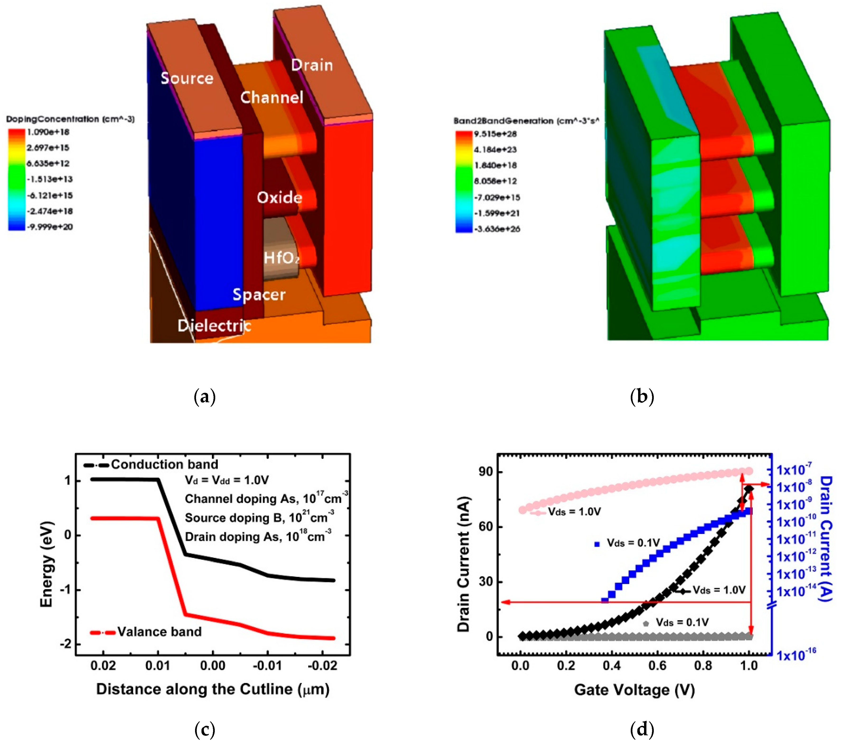
2. Three-Dimensional (3D) Device and Methodology

Figure 1 shows the 3D structure of a 3-nm node NS-TFET in Synopsys Sentaurus TCAD software (Synopsys, Mountain View, CA, USA) that was used to simulate an NS-TFET providing model incidents on a silicon semiconductor [28]. Design specifications were determined according to the international technology roadmap for 2015 [29]. Gate length (Lg) was set to 10 nm. Channel width (Tw) and channel thickness (Tch) were 16 and 5 nm, respectively. The contact distance from the middle of the source to that of the drain was 23.5 nm. Effective oxide thickness (EOT) was set to 0.68 nm (Tox = 0.43 nm, Thk = 1.4 nm), ensuring gate controllability. Doping at the source, drain and channel were set to 1021 cm−3 boron, 1018 cm−3 arsenic, and 1017 cm−3 arsenic, respectively. Note that while optimizing the doping concentration can further improve a device’s T-FET performance, there is no significant change in the behavior of the alpha particles when compared to conventional DD-FET. Contact resistance was set to 3 × 10⁻⁹ Ohm/cm2 considering latest process technology. Threshold voltage was controlled by the gate work function of the gate electrode material.
For implementation of the alpha-particle behavior in the 3-nm-node NS-TFET in Synopsys’ TCAD, a drift-diffusion approximation was used for the carrier transport. In addition to a non-local tunneling model and alpha particle incidence dimension, the current-voltage measured data of fabricated 14-nm bulk FinFET was used to calibrate the TCAD model. First, the 3D structure of the mobility degradation was plotted using a Lombardi method along with a thin-layer mobility model, as outlined in a previous work [25]. Next, the calibrated model parameters were applied to our TCAD simulation for the 3-nm NS-TFET.
In order to observe the alpha particle behavior incident on the NS-TFET, a test was performed by changing the points of incidence, angles of incidence, and temperature. The points of incidence were the source, drain, and channel regions; the angles of incidence was 30–90°; and the alpha particle energy was designated as 1–10 MeV. To take into account the carrier temperature, the hydro-dynamic model was turned on in the physics section of the TCAD. In addition, a non-local band-to-band tunneling model was used to consider the tunneling current dependency on the band edge profile along the entire path between the points connected by tunneling [30]. The device dimension and simulation conditions are listed in Table 1, and the doping concentration and band-to-band tunneling generation are described in Figure 1a,b, respectively. The following graph, Figure 1c, is a band diagram to determine if a device is acting as a tunneling FET. The valance and conduction bands in Figure 1c are bent to allow tunneling between bands between the source and channel [31,32,33,34]. In addition, Figure 1d shows the characteristics of Ids-Vgs. When the current values of Vds = 1.0 V and Vds = 0.1 V are compared with Vgs = 1.0 V, the difference of the current value between the two different Vds is 80.5 nA.

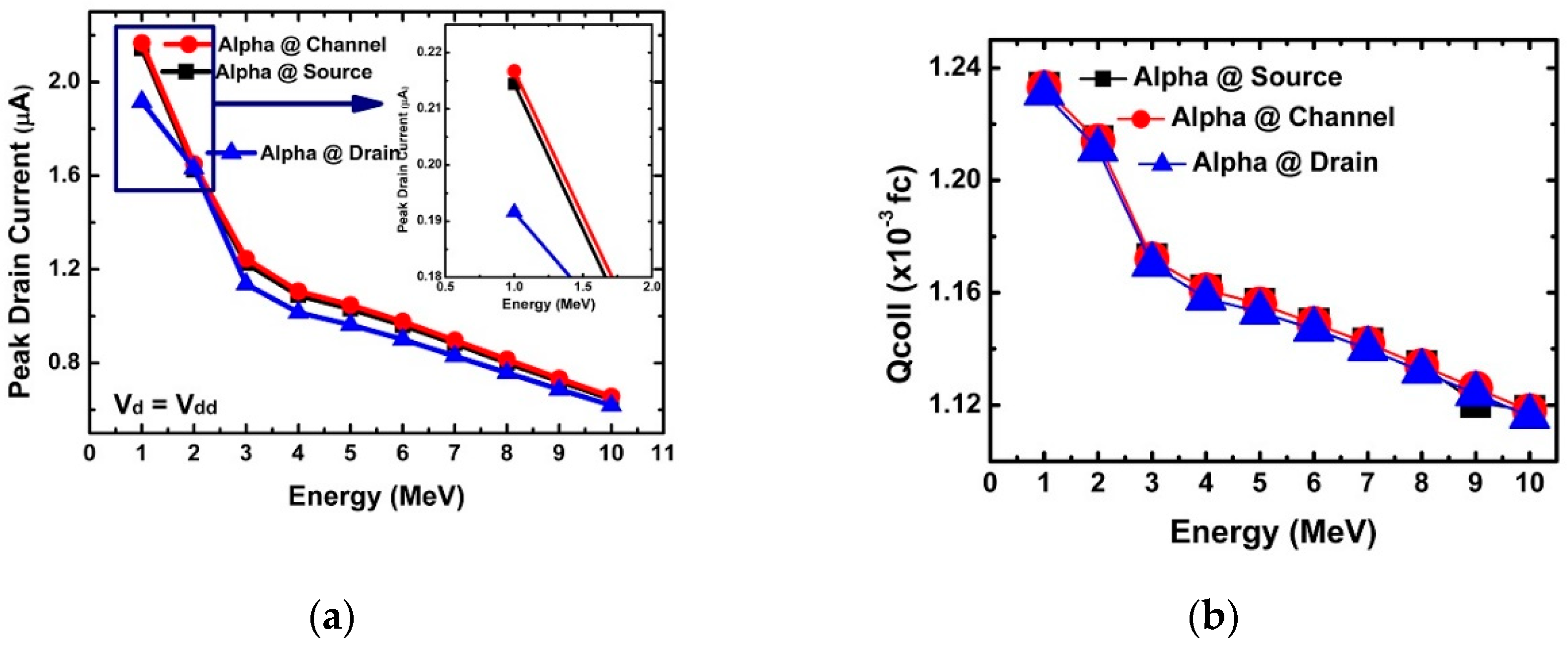
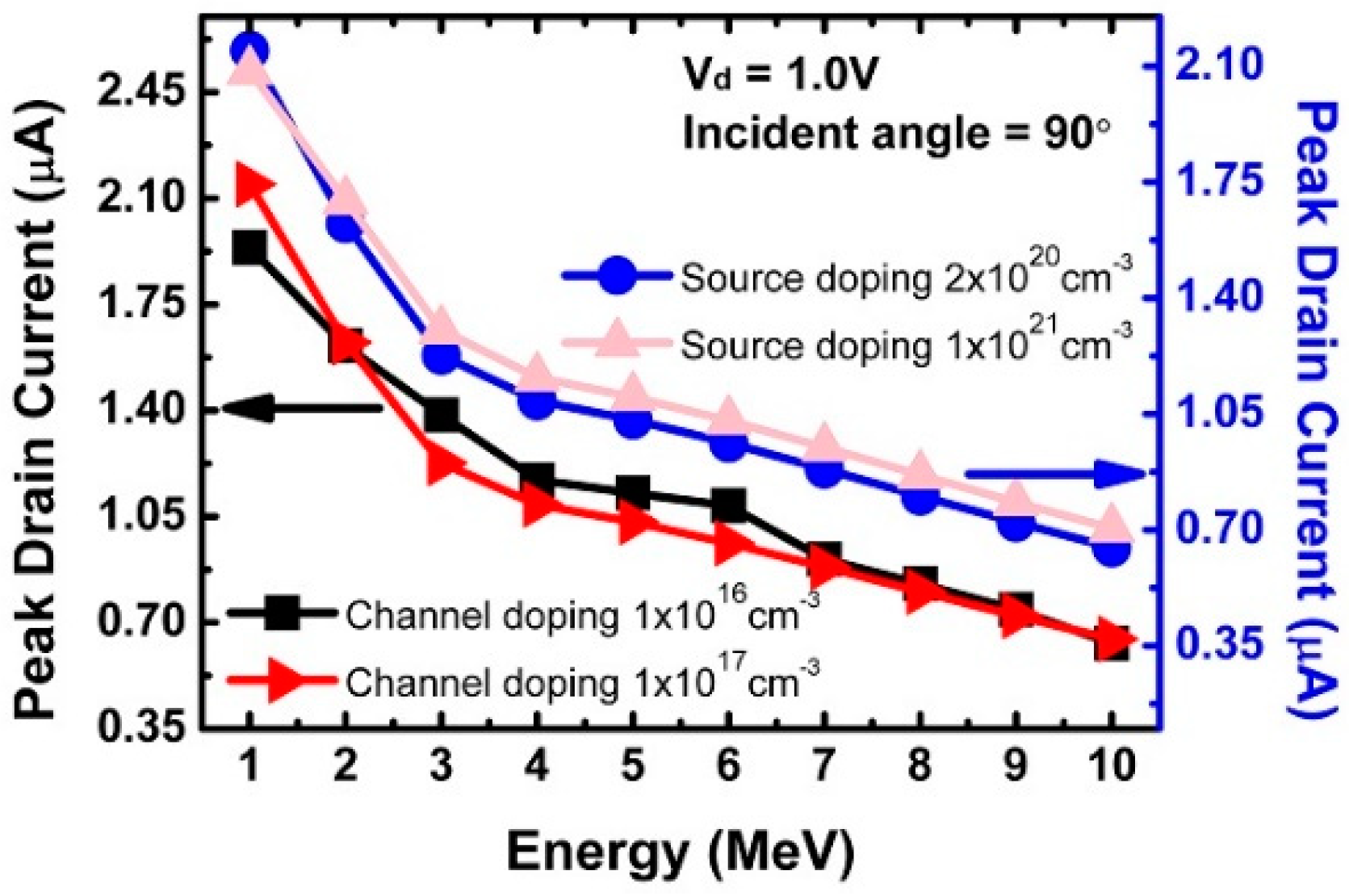
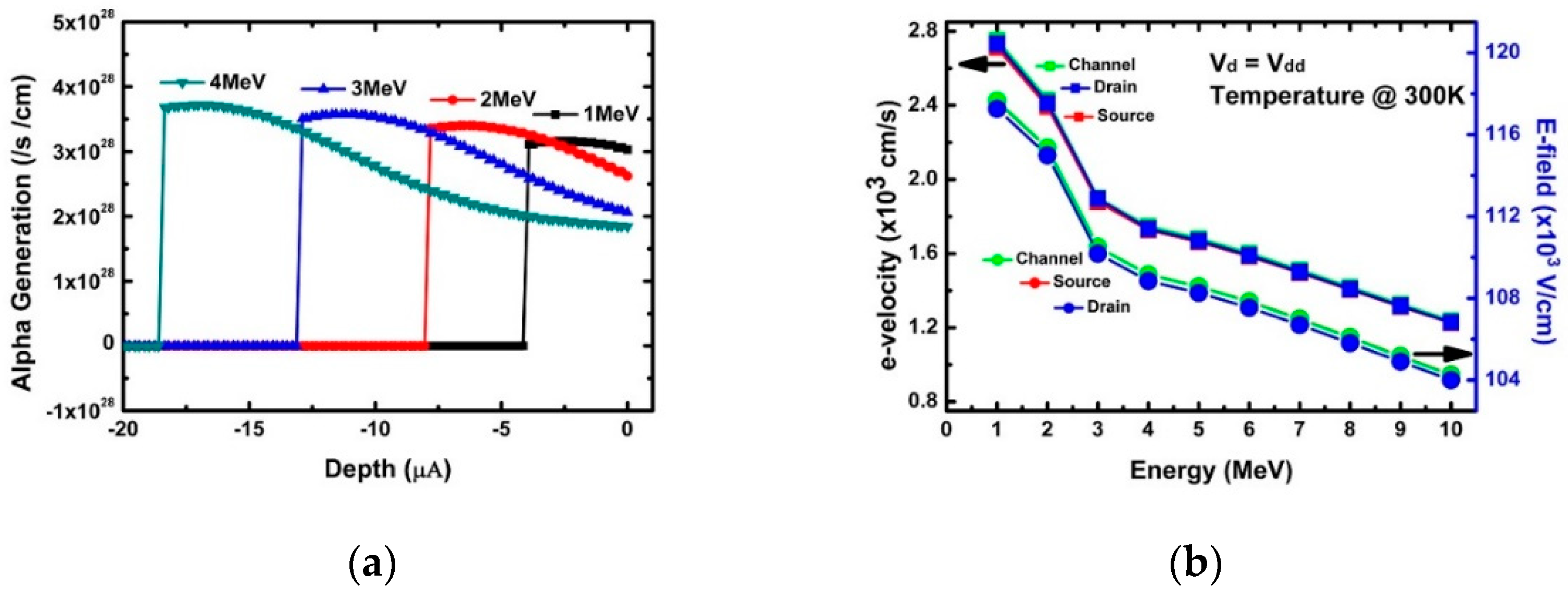
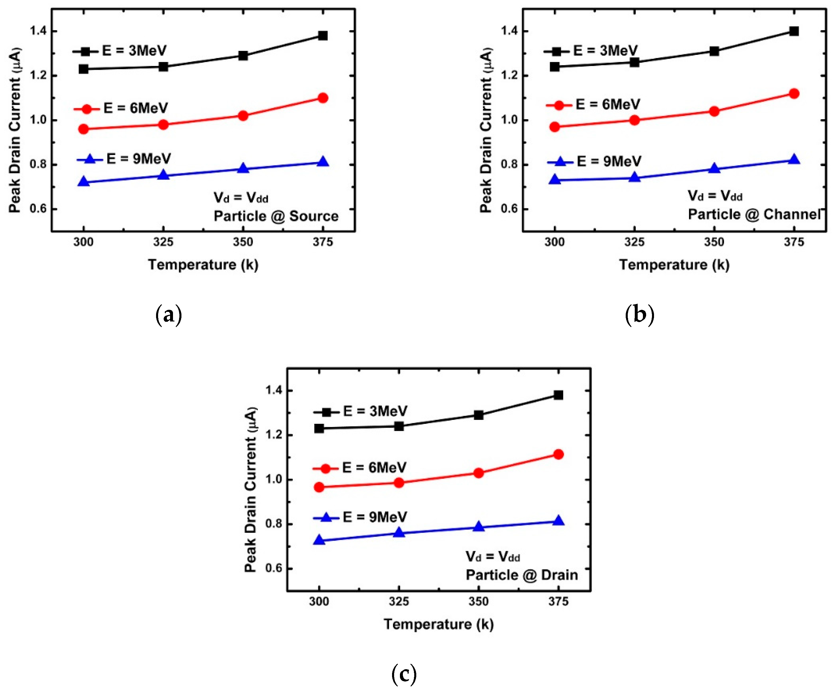
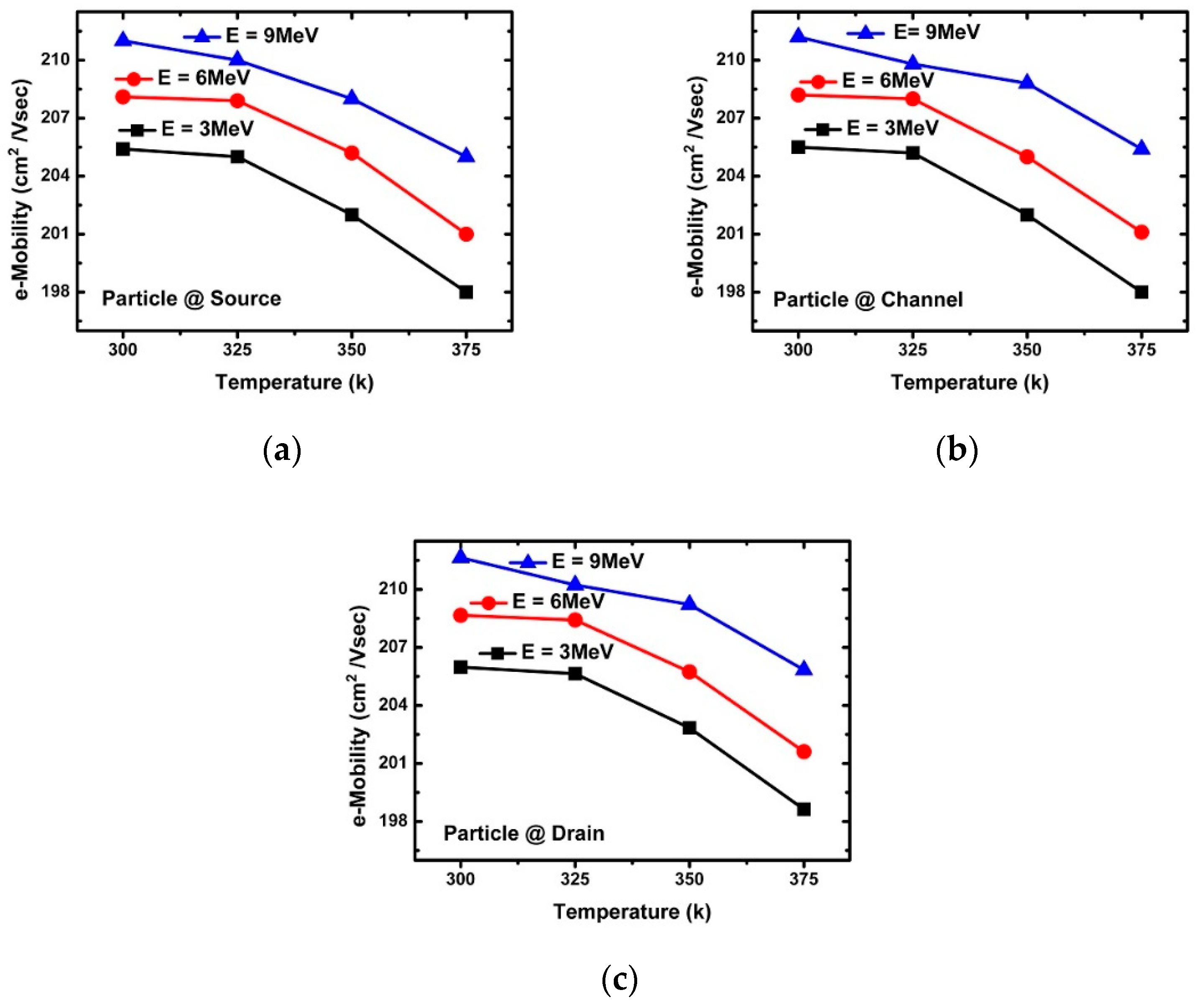
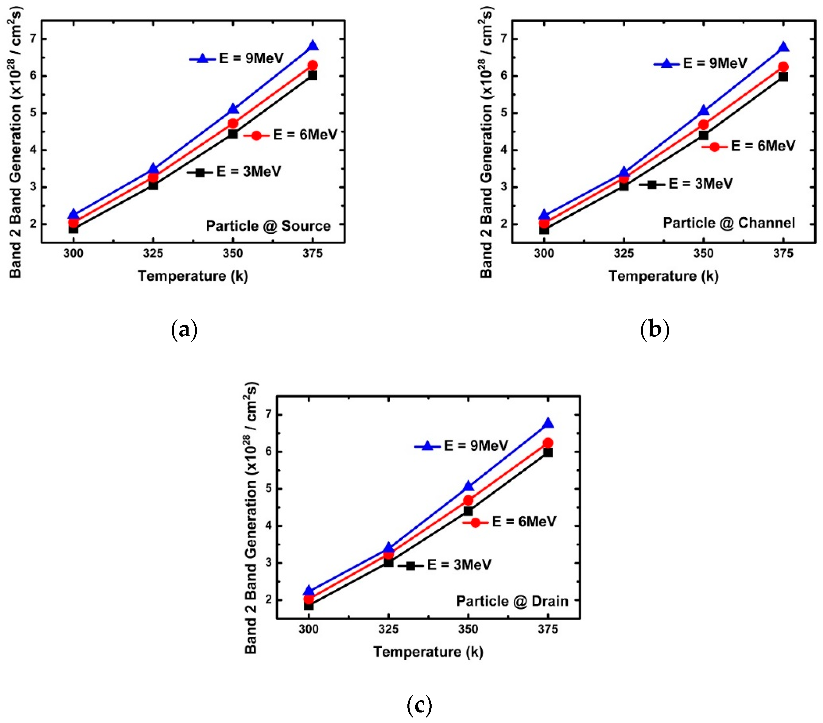
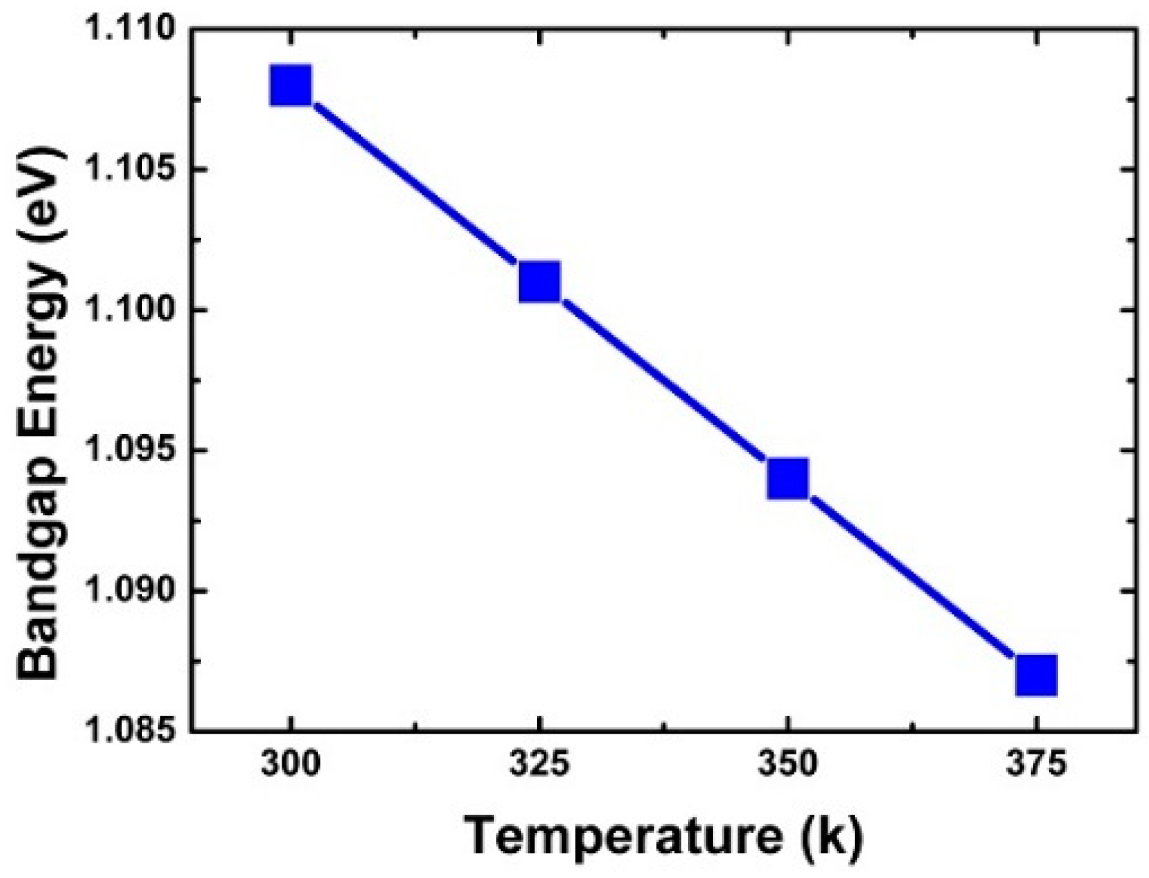
3. Results and Discussion

Figure 2a shows the variation of the drain current over time when an alpha particle enters the NS-TFET. This experiment is the result of injecting an alpha particle into the center of the source region with 5 MeV energy at t = 200 ps when the NS-TFET channel is in inversion and operating in the saturation region. When the alpha particle was injected, electron hole pair (EHP) generation occurred along the incident path, and the generated EHP contributed to the drain current component according to the electric field profile inside the NS-TFET. The drain current fluctuations increased during the short time period just after the alpha particle was injected, then returned to a steady state due to EHP recombination. At that time, not all EHPs generated by the alpha particles contributed to the drain current, and only the surviving carriers contributed to the current without recombination before the generated EHP reached the drain region. It was expected that the magnitude of the peak drain current due to the alpha particles would be much larger than the steady-state current (see Figure 2) and cause circuit malfunction. The inset in Figure 2 shows the peak drain current according to the alpha particle incidence angle. The closer the incidence angle was to the vertical, the larger the peak drain current became. Figure 2a marks the time duration. When the incidence position was applied to the source, channel, and drain, the time duration value according to the incident energy was almost take the same, as shown in Figure 2b. It can be observed in Figure 2b that the time duration also decreased as the incident energy increased. The graph in Figure 2b depicts how the time duration value decreased as the energy increased which is similar to Figure 3a that depicts how the peak drain current decreased with the incident energy. Therefore, there is a correlation between the amount of EHP generated by alpha particle incidence, which affects the peak drain current according to alpha particle incidence [35,36,37,38,39].
Figure 4 shows peak drain current with different doping concentration when the source was fixed to 1 × 1020 cm−3 and the doping concentration of the channel was set to 1 × 10¹⁶ and 1 × 1017 cm−3. When the energy was its lowest, the device with the higher doping concentration showed a higher peak drain current. The doping concentration of the source was doped into 2 × 10²⁰ and 1 × 1021 cm−3, and the channel was fixed at 1 × 1017 cm−3. In the different source doping concentration case, the peak drain current was high at the low doping concentration when the incident energy was 1 MeV. However, it was confirmed that both trends reversed as the incident energy surpassed 2 MeV.
Figure 3a,b shows the variation of the peak drain current and collected charge according to the incidence point and incident energy of the alpha particles. The collected charge can be obtained by integrating the current variation over time. Figure 3a shows that when the alpha particles were injected into the channel and source regions, they had a larger peak drain current than when they were injected into the drain, which was the opposite of a conventional DD-FET. For a DD-FET, the influence of the alpha particle injection into the drain is greater than at the source and channel regions [31]. It can be interpreted that the variation of EHP concentration in the channel and source regions has a big influence on the T-FET current because tunneling between the channel and source is the most important factor in determining the drain current in T-FETs.
In addition, Figure 3 shows that the peak drain current and collected charge decreased as the energy of the incident alpha particle increased. This can be explained by the EHP generation trend according to particle energy, as shown in Figure 5a. It can be seen that as the particle energy increased, the area where peak EHP was generated became further away from the incident point. Therefore, it can be concluded that EHPs generated by high particle energy cannot contribute to drain current fluctuations because EHPs generated by particles recombine before reaching the drain region. Drain current fluctuations are affected by electric field and carrier velocity fluctuations in addition to the EHP density generated by alpha particles [25]. Figure 5b shows electron velocity (e-velocity) and an electric-field (E-field) variations inside the NS-TFET according to particle energy. As the particle energy increased, both the e-velocity and E-field decreased, which is different from the vertical-FET (V-FET) result [25]. In V-FET, the higher particle energy increases both values. However, the results of this work are the same as for the device where the source and drain are located in the horizontal direction, as with common FinFETs.
Figure 3a confirms the change of the peak drain current according to energy. The decrease in peak drain current with increasing incident energy was found to be greatly affected by the penetration depth, e-velocity, and E-field of the incident alpha particles. Figure 5, Figure 6, Figure 7, Figure 8 and Figure 9 reflect a change in temperature. Figure 5, Figure 6, Figure 7, Figure 8 and Figure 9 show that all the electrical behaviors of various injected particle energies had the same trend for three incident energies. Figure 6 shows the results of alpha particle effects at various ambient temperature conditions. In the experiment of ambient temperature variation, the alpha particle effect was observed by varying the point of particle incidence and incident particle energy, the channel of the NS-TFET was strongly inverted, and the NS-TFET operated in the saturation region. It can be observed in Figure 6 that the peak drain current caused by the alpha particles increased when the ambient temperature increased. This result is the opposite of a previous work regarding FinFET and V-FET [25]. To analyze the results, we plotted electron mobility (e-mobility) and Shockley–Read–Hall (SRH) recombination according to ambient temperature, as shown in Figure 7 and Figure 8, respectively. As the ambient temperature increased, e-mobility decreased and SRH recombination increased. This is the same result as FinFET and V-FET [25]. Note that in this work, the used TCAD mobility model and parameters were taken from [25]. Although the temperature dependence of NS-TFET’s e-mobility and SRH recombination was the same as that of FinFET and V-FET, bandgap energy was analyzed to identify why the temperature dependence of the alpha particle of the NS-TFET was different from that of FinFET and V-FET. As the ambient temperature increased, the bandgap energy decreases, as shown in Figure 10. Furthermore, as the bandgap energy decreased, band-to-band tunneling between the source and channel increased, as shown in Figure 9. Therefore, the increase in peak drain current according to alpha particles and temperature can be explained by an increase in the tunneling current in NS-TFET resulting from the bandgap narrowing effect.

4. Conclusions

In this work, we analyzed the radiation effect caused by alpha particles in multi-nanosheet tunneling-TFET (NS-TFET) in a 3-nm technology node using 3D TCAD simulation. Due to the stacked multi-nanosheet structure and carrier transport of the tunneling mechanism in a lateral direction, the drain current variation was different from that of FinFET and V-FET when alpha particles are injected into the NS-TFET. First, when the alpha particle is injected into the channel and source regions, the effects of radiation are greater than when they are injected into the drain region. Second, the peak drain current fluctuation due to alpha particles decreases monotonically according to the incident energy. Third, as the ambient temperature increases, the peak drain current fluctuation increases monotonically due to the alpha particles. As a result of analyzing various physical characteristics through 3D TCAD, it has been observed that these characteristics are unique radiation characteristics shown by the structure and carrier transport of NS-TFET. Therefore, it can be seen that a design method different from the previous DD-based FETs is required for the development of integrated circuits that are resistant to radiation using NS-TFETs.

Author Contributions

Methodology, software, validation, resources, data curation, formal analysis, visualization, writing—original draft preparation, J.H. (Jungmin Hong), J.P., J.L., J.H. (Jeonghun Ham) and K.P.; writing—review and editing, conceptualization, investigation, supervision, project administration, funding acquisition, J.J.

Funding

This research was supported by the MOTIE (Ministry of Trade, Industry & Energy (10085645) and KSRC (Korea Semiconductor Research Consortium) support program for the development of future semiconductor devices, and in part, by the Korea Electric Power Corporation. (Grant No. R18XA06-78).

Acknowledgments

The EDA tool was supported by the IC Design Education Center (IDEC), Korea.

Conflicts of Interest

The authors declare no conflict of interest.

References

  1. Huang, X.; Zeng, Z.Y.; Zhang, H. Metal dichalcogenide nanosheets: Preparation, properties and applications. Chem. Soc. Rev. 2013, 42, 1934–1946. [Google Scholar] [CrossRef] [PubMed]
  2. Seo, Y.; Kim, S.; Ko, K.; Woo, C.; Kim, M.; Lee, J.; Kang, M.; Shin, H. Analysis of electrical characteristics and proposal of design guide for ultra-scaled nanoplate vertical FET and 6T-SRAM. Solid State Electron. 2018, 140, 69–73. [Google Scholar] [CrossRef]
  3. Kim, H.; Son, D.; Myeong, I.; Ryu, D.; Park, J.; Kang, M.; Jeon, J.; Shin, H. Strain Engineering for 3.5-nm Node in Stacked-Nanoplate FET. IEEE Trans. Electron Devices 2019, 66, 2898–2903. [Google Scholar] [CrossRef]
  4. Jeong, J.; Yoon, J.S.; Lee, S.; Baek, R.H. The Effects of Realistic U-shaped Source/Drain on DC/AC Performances of Silicon Nanosheet FETs for Sub 5-nm Node SoC Applications. In Proceedings of the 2019 Electron Devices Technology and Manufacturing Conference (EDTM), Singapore, 12–15 March 2019; pp. 133–135. [Google Scholar]
  5. Li, H.H.; Lin, Y.R.; Wu, Y.C.; Lin, Y.H.; Yu, J.J. Multi-stacking hybrid P/N/P nanosheet layers junctionless field-effect transistors. In Proceedings of the 2018 7th International Symposium on Next Generation Electronics (ISNE) IEEE, Taipei, Taiwan, 7–9 May 2018; pp. 1–3. [Google Scholar]
  6. Hossain, N.M.; Quader, S.; Siddik, A.B.; Chowdhury, M.I.B. TCAD based performance analysis of junctionless cylindrical double gate all around FET up to 5nm technology node. In Proceedings of the 2017 20th International Conference of Computer and Information Technology (ICCIT) IEEE, Dhaka, Bangladesh, 22–24 December 2017; pp. 1–4. [Google Scholar]
  7. Chen, G.; Li, M.; Fan, J.; Yang, Y.; Zhang, H.; Huang, R. Multi-V T design of vertical channel nanowire FET for sub-10nm technology node. In Proceedings of the 2016 IEEE International Nanoelectronics Conference (INEC) IEEE, Chengdu, China, 9–11 May 2016; pp. 1–2. [Google Scholar]
  8. Tsai, M.J.; Peng, K.H.; Lin, Y.R.; Wu, Y.C. Comparison of Vertically Double Stacked Poly-Si Nanosheet Junctionless Field Effect Transistors with Gate-all-around and Multi-gate Structure. In Proceedings of the 2019 International Symposium on VLSI Technology, Systems and Application (VLSI-TSA) IEEE, Hsinchu, Taiwan, 22–25 April 2019; pp. 1–2. [Google Scholar]
  9. Choi, W.Y.; Park, B.G.; Lee, J.D.; Liu, T.J.K. Tunneling field-effect transistors (TFETs) with subthreshold swing (SS) less than 60 mV/dec. IEEE Electron Device Lett. 2007, 28, 743–745. [Google Scholar] [CrossRef]
  10. Zhang, Q.; Zhao, W.; Seabaugh, A. Low-subthreshold-swing tunnel transistors. IEEE Electron Device Lett. 2006, 27, 297–300. [Google Scholar] [CrossRef]
  11. Krupkina, T.Y.; Artamonova, E.A.; Krasukov, A.Y.; Losev, V.V.; Solovev, A.V. TCAD simulation of TFET structures integrated in basic CMOS technology. In Proceedings of the 2017 IEEE Conference of Russian Young Researchers in Electrical and Electronic Engineering (EIConRus) IEEE, St. Petersburg, Russia, 1–3 February 2017; pp. 471–474. [Google Scholar]
  12. Chen, F.; Ilatikhameneh, H.; Tan, Y.; Klimeck, G.; Rahman, R. Switching Mechanism and the Scalability of vertical-TFETs. IEEE Trans. Electron Devices 2018, 65, 3065–3068. [Google Scholar] [CrossRef] [Green Version]
  13. Avci, U.E.; Morris, D.H.; Young, I.A. Tunnel field-effect transistors: Prospects and challenges. IEEE J. Electron Devices Soc. 2015, 3, 88–95. [Google Scholar] [CrossRef]
  14. Pradhan, K.P.; Sahu, P.K. Heavy-Ion Irradiation effect in trigate SOI tunnel FETs with High-k Spacer technology. In Proceedings of the 2016 IEEE Region 10 Conference (TENCON) IEEE, Singapore, 22–25 November 2016; pp. 2373–2376. [Google Scholar]
  15. Kim, J.; Lee, J.S.; Han, J.W.; Meyyappan, M. Single-event transient in FinFETs and nanosheet FETs. IEEE Electron Device Lett. 2018, 39, 1840–1843. [Google Scholar] [CrossRef]
  16. Wang, Q.; Liu, H.; Wang, S.; Chen, S. TCAD simulation of single-event-transient effects in L-shaped channel tunneling field-effect transistors. IEEE Trans. Nucl. Sci. 2018, 65, 2250–2259. [Google Scholar] [CrossRef]
  17. Black, J.D.; Ball Ii, D.R.; Robinson, W.H.; Fleetwood, D.M.; Schrimpf, R.D.; Reed, R.A.; Black, D.A.; Warren, K.M.; Tipton, A.D.; Dodd, P.E.; et al. Characterizing SRAM single event upset in terms of single and multiple node charge collection. IEEE Trans. Nucl. Sci. 2008, 55, 2943–2947. [Google Scholar] [CrossRef]
  18. Liu, T.; Liu, J.; Xi, K.; Zhang, Z.; He, D.; Ye, B.; Ying, Y.; Ji, Q.; Wang, B.; Luo, J.; et al. Heavy Ion Radiation Effects on a 130-nm COTS NVSRAM Under Different Measurement Conditions. IEEE Trans. Nucl. Sci. 2018, 65, 1119–1126. [Google Scholar] [CrossRef]
  19. Edwards, R.; Dyer, C.; Normand, E. Technical standard for atmospheric radiation single event effects (SEE) on avionics electronics. In Proceedings of the 2004 IEEE Radiation Effects Data Workshop (IEEE Cat. No. 04TH8774) IEEE, Atlanta, GA, USA, 22 July 2004; pp. 1–5. [Google Scholar]
  20. Torres, H.L.F.; Martino, J.A.; Rooyackers, R.; Vandooren, A.; Simoen, E.; Claeys, C.; Agopian, P.G.D. Proton radiation effects on the self-aligned triple gate SOI p-type tunnel FET output characteristic. In Proceedings of the 2017 32nd Symposium on Microelectronics Technology and Devices (SBMicro) IEEE, Fortaleza, Brazil, 28 August–1 September 2017; pp. 1–4. [Google Scholar]
  21. Cao, J.; Xu, L.; Bhuva, B.L.; Wen, S.J.; Wong, R.; Narasimham, B.; Massengill, L.W. Alpha Particle Soft-Error Rates for D-FF Designs in 16-Nm and 7-Nm Bulk FinFET Technologies. In Proceedings of the 2019 IEEE International Reliability Physics Symposium (IRPS) IEEE, Monterey, CA, USA, 31 March–4 April 2019; pp. 1–5. [Google Scholar]
  22. Munteanu, D.; Autran, J.L. Modeling and simulation of single-event effects in digital devices and ICs. IEEE Trans. Nucl. Sci. 2008, 55, 1854–1878. [Google Scholar] [CrossRef]
  23. Uemura, T.; Lee, S.; Min, D.; Moon, I.; Lim, J.; Lee, S.; Sagong, H.C.; Pae, S. Investigation of alpha-induced single event transient (SET) in 10 nm FinFET logic circuit. In Proceedings of the 2018 IEEE International Reliability Physics Symposium (IRPS), IEEE, Burlingame, CA, USA, 11–15 March 2018; p. P-SE. [Google Scholar]
  24. Atkinson, N.M.; Ahlbin, J.R.; Witulski, A.F.; Gaspard, N.J.; Holman, W.T.; Bhuva, B.L.; Zhang, E.X.; Li, C.; Massengill, L.W. Effect of transistor density and charge sharing on single-event transients in 90-nm bulk CMOS. IEEE Trans. Nucl. Sci. 2011, 58, 2578–2584. [Google Scholar] [CrossRef]
  25. Seo, Y.; Kang, M.; Jeon, J.; Shin, H. Prediction of Alpha Particle Effect on 5-nm Vertical Field-Effect Transistors. IEEE Trans. Electron Devices 2018, 66, 806–809. [Google Scholar] [CrossRef]
  26. Dodd, P.E. Physics-based simulation of single-event effects. IEEE Trans. Device Mater. Reliab. 2005, 5, 343–357. [Google Scholar] [CrossRef]
  27. Xiao, S.; Minfeng, Y.; Yanfei, Z.; Lixin, W.; Mengxin, L. Anti-Single-Event Technology Based on the Novel Hole-Current Diversionary Structure. In Proceedings of the 2018 14th IEEE International Conference on Solid-State and Integrated Circuit Technology (ICSICT) IEEE, Qingdao, China, 31 October–3 November 2018; pp. 1–3. [Google Scholar]
  28. Wu, Y.C.; Jhan, Y.R. Introduction of synopsys sentaurus TCAD simulation. In 3D TCAD Simulation for CMOS Nanoeletronic Devices; Springer: Singapore, 2018; pp. 1–17. [Google Scholar]
  29. International Technology Roadmap for Semiconductors (ITRS). Available online: http://www.itrs2.net/ (accessed on 5 June 2015).
  30. Biswas, A.; Dan, S.S.; Le Royer, C.; Grabinski, W.; Ionescu, A.M. TCAD simulation of SOI TFETs and calibration of non-local band-to-band tunneling model. Microelectron. Eng. 2012, 98, 334–337. [Google Scholar] [CrossRef]
  31. Villalon, A.; Le Carval, G.; Martinie, S.; Le Royer, C.; Jaud, M.A.; Cristoloveanu, S. Further insights in TFET operation. IEEE Trans. Electron Devices 2014, 61, 2893–2898. [Google Scholar] [CrossRef]
  32. Singh, P.K.; Kumar, S.; Chander, S.; Baral, K.; Jit, S. Impact of Strain on Electrical Characteristic of Double-Gate TFETs with a SiO 2/RfO 2 Stacked Gate-Oxide Structure. In Proceedings of the 2017 14th IEEE India Council International Conference (INDICON) IEEE, Roorkee, India, 15–17 December 2017; pp. 1–5. [Google Scholar]
  33. Britnell, L.; Gorbachev, R.V.; Jalil, R.; Belle, B.D.; Schedin, F.; Mishchenko, A.; Georgiou, T.; Katsnelson, M.I.; Eaves, L.; Morozov, S.V.; et al. Field-effect tunneling transistor based on vertical graphene heterostructures. Science 2012, 335, 947–950. [Google Scholar] [CrossRef] [Green Version]
  34. Kumar, M.J.; Janardhanan, S. Doping-less tunnel field effect transistor: Design and investigation. IEEE Trans. Electron Devices 2013, 60, 3285–3290. [Google Scholar] [CrossRef] [Green Version]
  35. Yang, J.; Wang, P.; Zhang, Y.; Cheng, Y.; Zhao, W.; Chen, Y.; Li, H.H. Radiation-induced soft error analysis of STT-MRAM: A device to circuit approach. IEEE Trans. Comput. Aided Des. Integr. Circuits Syst. 2015, 35, 380–393. [Google Scholar] [CrossRef]
  36. Wrobel, F.; Dilillo, L.; Touboul, A.D.; Saigné, F. Comparison of the transient current shapes obtained with the diffusion model and the double exponential law—Impact on the SER. In Proceedings of the 2013 14th European Conference on Radiation and Its Effects on Components and Systems (RADECS) IEEE, Oxford, UK, 23–27 September 2013; pp. 1–4. [Google Scholar]
  37. Raji, M.; Sabet, M.A.; Ghavami, B. Soft error reliability improvement of digital circuits by exploiting a fast gate sizing scheme. IEEE Access 2019, 66485–66495. [Google Scholar] [CrossRef]
  38. Nicolaidis, M. Time redundancy based soft-error tolerance to rescue nanometer technologies. In Proceedings of the 17th IEEE VLSI Test. Symposium (Cat. No. PR00146) IEEE, Dana Point, CA, USA, 25–29 April 1999; pp. 86–94. [Google Scholar]
  39. Gadlage, M.J.; Schrimpf, R.D.; Narasimham, B.; Pellish, J.A.; Warren, K.M.; Reed, R.A.; Weller, R.A.; Bhuva, B.L.; Massengill, L.W.; Zhu, X. Assessing alpha particle-induced single event transient vulnerability in a 90-nm CMOS technology. IEEE Electron Device Lett. 2008, 29, 638–640. [Google Scholar] [CrossRef]
Figure 1. (a) Structure and doping concentration of the 3-nm multi-nanosheet, (b) band-to-band tunneling generation, (c) energy band diagram and (d) Ids-Vgs transfer curve.
Micromachines 10 00847 g001
Figure 2. (a) Transient drain current of the multi-nanosheet tunneling-based field-effect transistor (NS-TFET) when an alpha particle is injected into the source region at t = 200 ps; (b) time duration with different particle energy injections at the source with an incident angle of 90°.
Micromachines 10 00847 g002
Figure 3. (a) Peak drain current with particle energy in different regions; (b) collected charges of different particle energy injections at the source, channel, and drain with an incident angle of 90°.
Micromachines 10 00847 g003
Figure 4. Peak drain current and particle energy in the source and channel regions by different source and channel doping concentrations.
Micromachines 10 00847 g004
Figure 5. (a) Generation distribution with energy of particles; (b) electric field and electron velocity at the top of the drain bulk with the different particle energies.
Micromachines 10 00847 g005
Figure 6. Peak drain current with three different alpha particle energy injections (3, 6, and 9 MeV) at the (a) source (b) channel, and (c) drain.
Micromachines 10 00847 g006
Figure 7. E-mobility with three different alpha particle energy injections (3, 6, and 9 MeV) at the (a) source, (b) channel, and (c) drain.
Micromachines 10 00847 g007
Figure 8. Shockley–Read–Hall (SRH) recombination with three different alpha particle energy injections (3, 6, and 9 MeV) at the (a) source, (b) channel, and (c) drain.
Micromachines 10 00847 g008
Figure 9. Band-to-band tunneling generation with three different alpha particle energy injections (3, 6, and 9 MeV) at the (a) source, (b) channel, and (c) drain.
Micromachines 10 00847 g009
Figure 10. Silicon energy bandgap with different temperatures.
Micromachines 10 00847 g010
Table 1. Used parameters for device geometry and alpha particle simulation, which correspond to the international technology roadmap for semiconductors (ITRS)-based 3-nm technology node scenario.
Device ParametersValueDevice ParametersValue
Gate length, Lg (nm)10Ambient temperature (K)300–375
Channel width, Tw (nm)16Alpha particle energy (MeV)1–10
Channel thickness, Tch (nm)5Incident angle (°)30–90
Contact gate pitch, CGP (nm)23.5Source doping (cm−3)B, 1021
Effective oxide thickness (nm)0.68Drain doping (cm−3)As, 1018
Contact resistance (Ω-cm−3)3 × 10⁻⁹Channel doping (cm−3)As, 1017
Gate voltage (Vg) (V)0–1.0Drain voltage (Vd) (V)0.1, 1.0

