Functional Metallic Microcomponents via Liquid-Phase Multiphoton Direct Laser Writing: A Review

Abstract
:1. Introduction
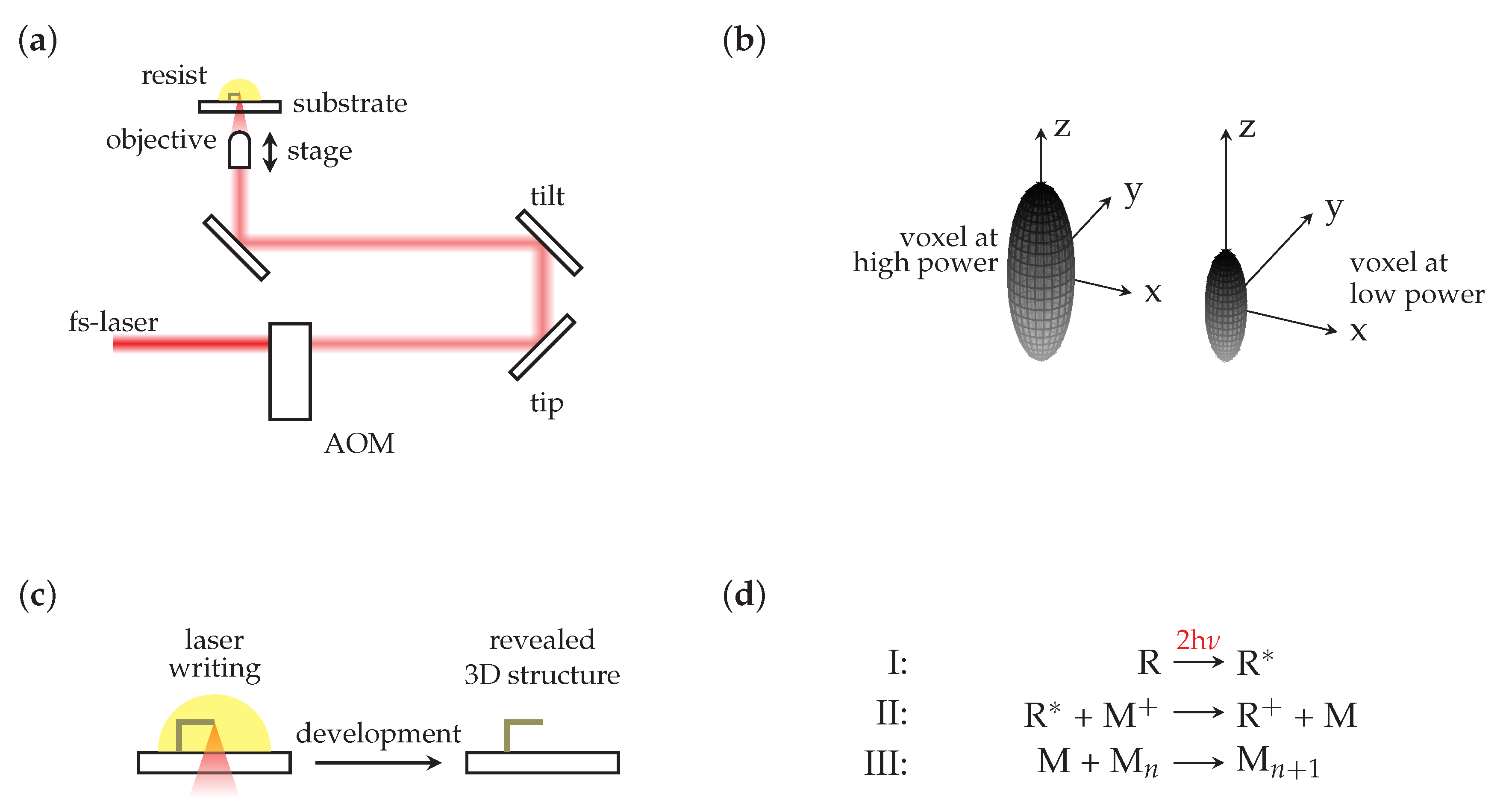
2. Short Introduction to Direct Laser Writing of Metallic Structures
3. Challenges of MDLW and Common Structure Properties
4. Functional Planar Metallic Microcomponents Fabricated by Direct Laser Writing
4.1. Electronic Components
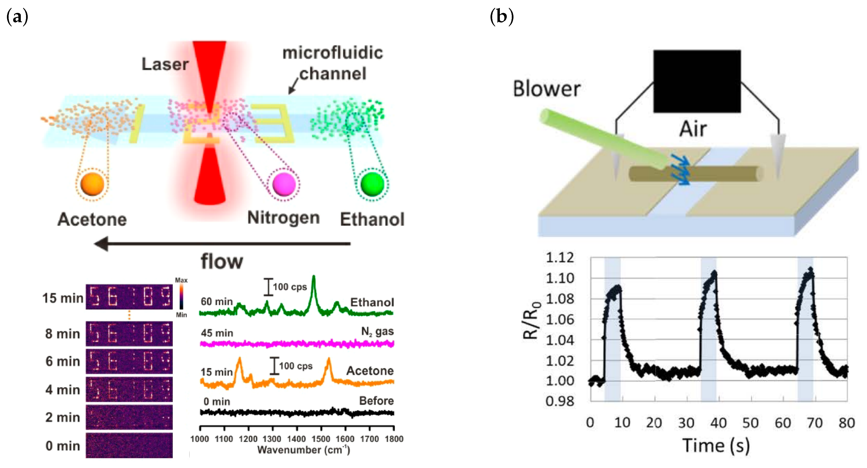
4.2. Sensors
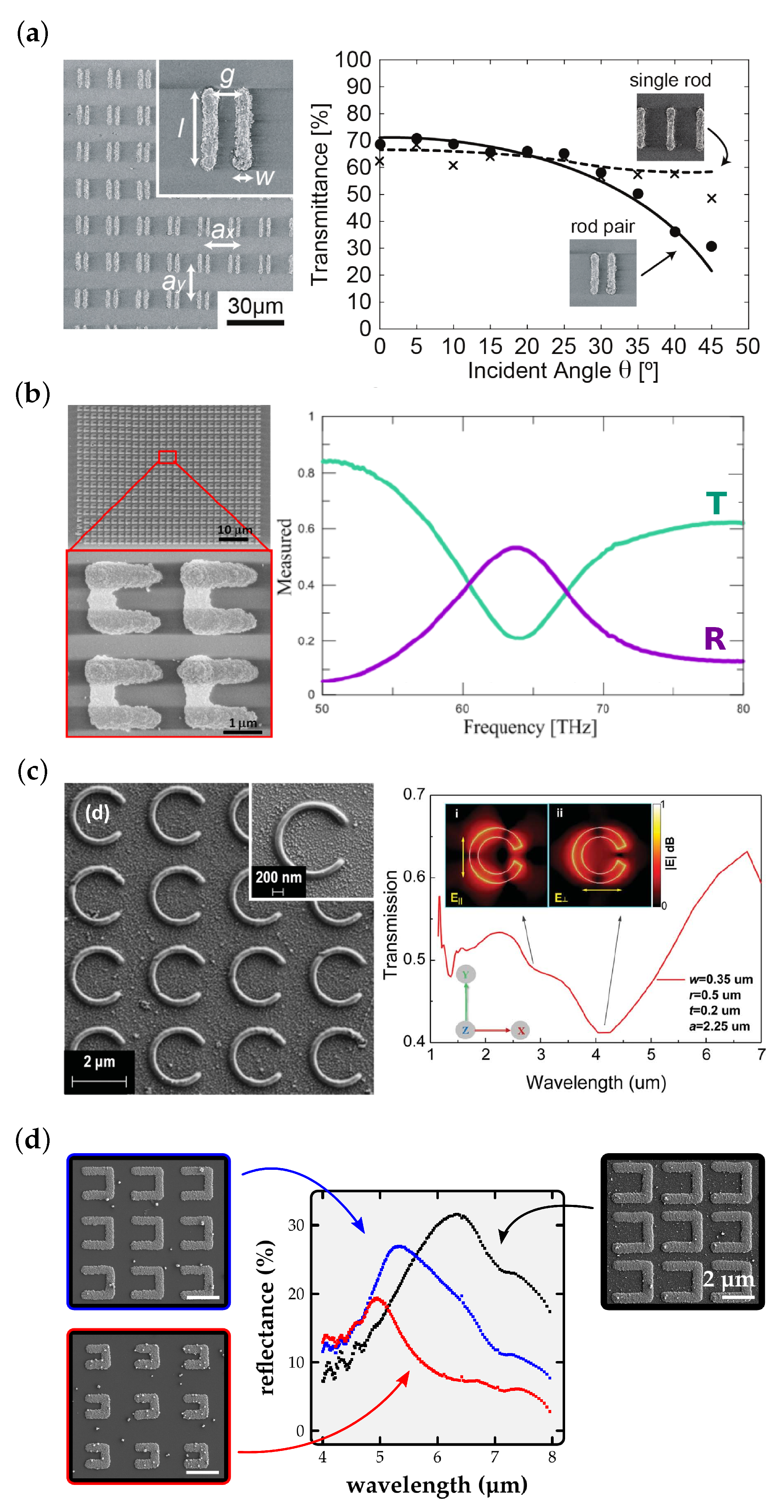
4.3. Metamaterials
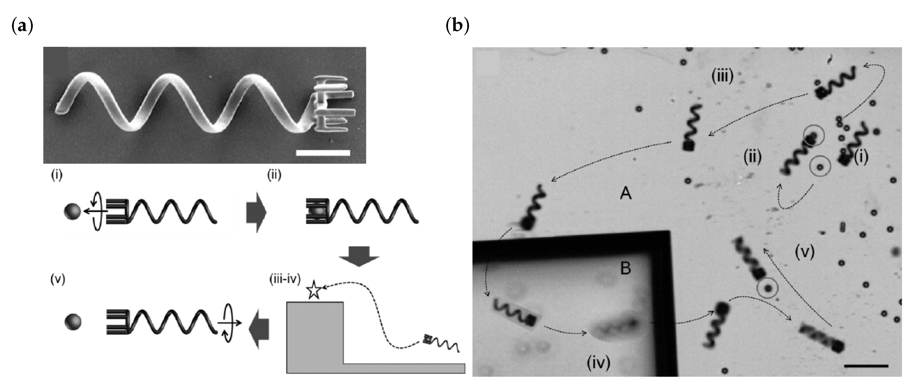
5. Functional 3D Metallic Microcomponents Fabricated by Direct Laser Writing
6. Conclusions
Author Contributions
Funding
Acknowledgments
Conflicts of Interest
Abbreviations
| MEMS | Microelectromechanical systems |
| HF | High-frequency |
| DIW | Direct ink writing |
| EHD | Electrohydrodynamic printing |
| LAED | Laser-assisted electrophoretic deposition |
| LIFT | Laser-induced forward transfer |
| MCE | Meniscus-confined electroplating |
| ELD | Electroplating of locally dispensed ions in liquid |
| DLW | Direct laser writing |
| MDLW | Metal direct laser writing |
| 3D | Three-dimensional |
| NA | Numerical aperture |
| AOM | Acousto-optical modulator |
| EDX | Energy-dispersive X-ray spectroscopy |
| PET | Polyethylene terephthalate |
| OFET | Organic field effect transistor |
| PMMA | Polymethyl methacrylate |
| SEM | Scanning electron microscopy |
| PDMS | Polydimethylsiloxane |
| ODMR | Optically detected magnetic resonance |
| SERS | Surface-enhanced Raman scattering |
| 4-MBT | 4-methylbenzenethiol |
| PVP | Poly(vinylpyrrolidone) |
| TE | Transversal electric |
| NDSS | N-decanoylsarcosine sodium |
| 2D | Two-dimensional |
| TGA | Thermogravimetric analysis |
| DSC | Differential scanning calorimetry |
| DLP | Digital light processing |
| PEGDA | Polyethylene glycol diacrylate |
References
- Vaezi, M.; Seitz, H.; Yang, S. A review on 3D micro-additive manufacturing technologies. Int. J. Adv. Technol. 2013, 67, 1721–1754. [Google Scholar]
- Lewis, J.A. Direct Ink Writing of 3D Functional Materials. Adv. Funct. Mater. 2006, 16, 2193–2204. [Google Scholar] [CrossRef]
- Onses, M.S.; Ferreira, P.M.; Alleyne, A.G.; Rogers, J.A. Mechanisms, Capabilities, and Applications of High-Resolution Electrohydrodynamic Jet Printing. Small 2015, 11, 4237–4266. [Google Scholar] [CrossRef] [PubMed]
- Takai, T.; Nakao, H.; Iwata, F. Three-dimensional microfabrication using local electrophoresis deposition and a laser trapping technique. Opt. Express 2014, 18, 28109–28117. [Google Scholar] [CrossRef] [PubMed]
- Kuznetsov, A.I.; Kiyan, R.; Chichkov, B.N. Laser fabrication of 2D and 3D metal nanoparticle structures and arrays. Opt. Express 2010, 18, 21198–21203. [Google Scholar] [CrossRef]
- Suryavanshi, A.P.; Yu, M.-F. Probe-based electrochemical fabrication of freestanding Cu nanowire array. Appl. Phys. Lett. 2006, 88, 083103. [Google Scholar] [CrossRef]
- Momotenko, D.; Page, A.; Adobes-Vidal, M.; Unwin, P.R. Write-Read 3D Patterning with a Dual-Channel Nanopipette. ACS Nano 2016, 10, 8871–8878. [Google Scholar] [CrossRef]
- Ladd, C.; So, J.-H.; Muth, J.; Dickey, M.D. 3D Printing of Free-Standing Liquid Metal Microstructures. Adv. Mater. 2013, 25, 5081–5085. [Google Scholar] [CrossRef]
- Parekh, D.P.; Ladd, C.; Panich, L.; Moussa, K.; Dickey, M.D. 3D printing of liquid metals as fugitive inks for fabrication of 3D microfluidic channels. Lab Chip 2016, 16, 1812–1820. [Google Scholar] [CrossRef]
- Farahani, R.D.; Dube, M.; Therriault, D. Three-Dimensional Printing of Multifunctional Nanocomposites: Manufacturing Techniques and Applications. Adv. Mater. 2016, 28, 5794–5821. [Google Scholar] [CrossRef]
- Hirt, L.; Reiser, A.; Spolenak, R.; Zambelli, T. Additive Manufacturing of Metal Structures at the Micrometer Scale. Adv. Mater. 2017, 29, 1604211. [Google Scholar] [CrossRef] [PubMed]
- LaFratta, C.N.; Fourkas, J.T.; Baldacchini, T.; Farrer, R.A. Multiphoton Fabrication. Angew. Chem. Int. Ed. 2007, 46, 6238–6258. [Google Scholar] [CrossRef] [PubMed]
- Hohmann, J.K.; Renner, M.; Waller, E.H.; von Freymann, G. Three-Dimensional µ-Printing: An Enabling Technology. Adv. Opt. Mater. 2015, 3, 1488–1507. [Google Scholar] [CrossRef]
- Barner-Kowollik, C.; Bastmeyer, M.; Blasco, E.; Delaittre, G.; Müller, P.; Richter, B.; Wegener, M. 3D Laser Micro- and Nanoprinting: Challenges for Chemistry. Angew. Chem. 2017, 56, 15828–15845. [Google Scholar] [CrossRef]
- Tanaka, T.; Ishikawa, A.; Kawata, S. Two-photon-induced reduction of metal ions for fabricating three-dimensional electrically conductive metallic microstructure. Appl. Phys. Lett. 2006, 88, 081107. [Google Scholar] [CrossRef]
- Waller, E.H.; von Freymann, G. From photoinduced electron transfer to 3D metal microstructures via direct laser writing. Nanophotonics 2018, 7, 1259–1277. [Google Scholar] [CrossRef]
- Ishikawa, A.; Tanaka, T.; Kawata, S. Improvement in the reduction of silver ions in aqueous solution using two-photon sensitive dye. Appl. Phys. Lett. 2006, 89, 113102. [Google Scholar] [CrossRef]
- Auyeung, R.C.Y.; Kim, H.; Mathews, S.A.; Pique, A. Laser Direct-Write of Metallic Nanoparticle Inks. JLMN 2007, 2, 21–25. [Google Scholar] [CrossRef]
- Maruo, S.; Saeki, T. Femtosecond laser direct writing of metallic microstructures by photoreduction of silver nitrate in a polymer matrix. Opt. Express 2007, 16, 1174–1179. [Google Scholar] [CrossRef]
- Cao, Y.; Takeasu, N.; Tanaka, T.; Duan, X.; Kawata, S. 3D metallic nanostructure fabrication by surfactant-assisted multiphoton-induced reduction. Small 2009, 5, 1144–1148. [Google Scholar] [CrossRef]
- Kang, S.Y.; Vora, K.; Mazur, E. One-step direct-laser metal writing of sub-100nm 3D silver nanostructures in a gelatin matrix. Nanotechnology 2015, 26, 121001. [Google Scholar] [CrossRef] [PubMed]
- Ma, Z.-C.; Zhang, Y.-L.; Hang, B.; Chen, Q.-D.; Sun, H.-B. Femtosecond-Laser Direct Writing of Metallic Micro/Nanostructures: From Fabrication Strategies to Future Applications. Small Methods 2018, 2, 1700413. [Google Scholar] [CrossRef]
- LaFratta, C.N.; Lim, D.; O’Malley, K.; Baldacchini, T.; Fourkas, J.T. Direct Laser Patterning of Conductive Wires on Three-Dimensional Polymeric Microstructures. Chem. Mater. 2006, 18, 2038–2042. [Google Scholar] [CrossRef]
- Gansel, J.K.; Thiel, M.; Rill, M.S.; Decker, M.; Bade, K.; Saile, V.; von Freymann, G.; Linden, S.; Wegener, M. Gold Helix Photonic Metamaterial as Broadband Circular Polarizer. Science 2009, 325, 1513–1515. [Google Scholar] [CrossRef] [PubMed]
- Radke, A.; Gissibl, T.; Klotzbücher, T.; Braun, P.V.; Giessen, H. Three-Dimensional Bichiral Plasmonic Crystals Fabricated by Direct Laser Writing and Electroless Silver Plating. Adv. Mater. 2011, 23, 3018–3021. [Google Scholar] [CrossRef]
- Terzaki, K.; Vasilantonakis, N.; Gaidukeviciute, A.; Reinhardt, C.; Fotakis, C.; Vamvakaki, M.; Farsari, M. 3D conducting nanostructures fabricated using direct laser writing. Opt. Mater. Express 2011, 1, 586–597. [Google Scholar] [CrossRef]
- Vasilantonakis, N.; Terzaki, K.; Sakellari, I.; Purlys, V.; Gray, D.; Soukoulis, C.M.; Vamvakaki, M.; Kafesaki, M.; Farsari, M. Three-Dimensional Metallic Photonic Crystals with Optical Bandgabps. Adv. Mater. 2012, 24, 1101–1105. [Google Scholar] [CrossRef]
- Tottori, S.; Zhang, L.; Qiu, F.; Krawczyk, K.K.; Franco-Obregon, A.; Nelson, B.J. Magnetical Helical Micromachines: Fabrication, Controlled Swimming, and Cargo Transport. Adv. Mater. 2012, 24, 811–816. [Google Scholar] [CrossRef]
- Bagheri, S.; Weber, K.; Gissibl, T.; Weiss, T.; Neubrech, F.; Giessen, H. Fabrication of Square-Centimeter Plasmonic Nanoantenna Arrays by Femtosecond Direct Laser Writing Lithography: Effects of Collective Excitations on SEIRA Enhancement. ACS Photonics 2015, 2, 779–786. [Google Scholar] [CrossRef]
- Gu, X.W.; Greer, J.R. Ultra-strong architected Cu meso-lattices. Extrem. Mech. Lett. 2015, 2, 7–14. [Google Scholar]
- Faniayeu, I.; Mizeikis, V. Vertical split-ring resonator perfect absorber metamaterial for IR frequencies realized via femtosecond direct laser writing. Appl. Phys. Express 2017, 10, 062001. [Google Scholar] [CrossRef]
- Oran, D.; Rodriques, S.G.; Gao, R.; Asano, S.; Skylar-Scott, M.A.; Chen, F.; Tillberg, P.W.; Marblestone, A.H.; Boyden, E.S. 3D nanofabrication by volumetric deposition and controlled shrinkage of patterned scaffolds. Science 2018, 362, 1281–1285. [Google Scholar] [CrossRef] [PubMed]
- Xia, X.; Afshar, A.; Yang, H.; Portela, C.M.; Kochmann, D.M.; Di Leo, C.V.; Greer, J.R. Electrochemically reconfigurable architected materials. Nature 2019, 573, 205–213. [Google Scholar] [CrossRef] [PubMed]
- Maruo, S.; Nakamura, O.; Kawata, S. Three-dimensional microfabrication with two-photon-absorbed photopolymerization. Opt. Lett. 1997, 22, 132–134. [Google Scholar] [CrossRef] [PubMed] [Green Version]
- Jesacher, A.; Booth, M.J. Parallel direct laser writing in three dimensions with spatially dependent aberration correction. Opt. Express 2010, 18, 21090–21099. [Google Scholar] [CrossRef] [PubMed] [Green Version]
- Cumming, B.P.; Jesacher, A.; Booth, M.J.; Wilson, T.; Gu, M. Adaptive aberration compensation for three-dimensional micro-fabrication of photonic crystals in lithium niobate. Opt. Express 2011, 19, 9419–9425. [Google Scholar] [CrossRef] [PubMed]
- Waller, E.H.; Renner, M.; von Freymann, G. Active aberration- and point-spread-function control in direct laser writing. Opt. Express 2019, 20, 24949–24956. [Google Scholar] [CrossRef]
- Yang, L.; El-Tamer, A.; Hinze, U.; Li, J.; Hu, Y.; Huang, W.; Chu, J.; Chichkov, B.N. Parallel direct laser writing of micro-optical and photonic structures using spatial light modulator. Opt. Lasers Eng. 2015, 70, 26–32. [Google Scholar] [CrossRef]
- Fischer, J.; von Freymann, G.; Wegener, M. The Materials Challenge in Diffraction-Unlimited Direct Laser Writing Optical Lithograhpy. Adv. Mater. 2010, 22, 3578–3582. [Google Scholar] [CrossRef]
- Fischer, J.; Wegener, M. Three-dimensional optical laser lithography beyond the diffraction limit. Laser Photonics Rev. 2012, 7, 22–44. [Google Scholar] [CrossRef]
- Bückmann, T.; Stenger, N.; Kadic, M.; Kaschke, J.; Frölich, A.; Kennerknecht, T.; Eberl, C.; Thiel, M.; Wegener, M. Tailored 3D Mechnaical Metamaterials Made by Dip-in Direct-Laser-Writing Optical Lithography. Adv. Mater. 2012, 22, 2710–2714. [Google Scholar] [CrossRef] [PubMed]
- Mueller, P.; Thiel, M.; Wegener, M. 3D direct laser writing using a 405 nm diode laser. Opt. Lett. 2014, 39, 6847–6850. [Google Scholar] [CrossRef] [PubMed]
- Mayer, F.; Richter, S.; Westhauser, J.; Blasco, E.; Barner-Kowollik, C.; Wegener, M. Multimaterial 3D laser microprinting using an integrated microfluidic system. Sci. Adv. 2019, 5, eaau9160. [Google Scholar] [CrossRef] [PubMed] [Green Version]
- Hippler, M.; Blasco, E.; Qu, J.; Tanaka, M.; Barner-Kowollik, C.; Wegener, M.; Bastmeyer, M. Controlling the shape of 3D microstructures by temperature and light. Nat. Commun. 2019, 10, 232. [Google Scholar] [CrossRef] [Green Version]
- Tabrizi, S.; Cao, Y.Y.; Lin, H.; Jia, B.H. Two-photon reduction: A cost-effective method for fabrication of functional metallic nanostructures. Sci. China-Phys. Mech. Astron. 2017, 60, 034201. [Google Scholar] [CrossRef]
- He, G.; Zheng, M.; Dong, X.; Jin, F.; Liu, J.; Duan, X.; Zhao, Z. The Conductive Silver Nanowires Fabricated by Two-beam Laser Direct Writing on the Flexible Sheet. Sci. Rep. 2017, 7, 41757. [Google Scholar] [CrossRef]
- Xu, B.; Zhang, D.; Liu, X.; Wang, L.; Xu, W.; Haraguchi, M.; Li, A. Fabrication of microelectrodes based on precursor doped with metal seeds by femtosecond laser direct writing. Opt. Lett. 2014, 39, 434–437. [Google Scholar] [CrossRef]
- Xu, B.; Xia, H.; Niu, L.; Zhang, Y.; Sun, K.; Chen, Q.; Xu, Y.; Lv, Z.; Li, Z.; Misawa, H.; et al. Flexible Nanowiring of Metal on Nonplanar Substrates by Femtosecond-Laser-Induced Electroless Plating. Small 2010, 6, 1762–1766. [Google Scholar] [CrossRef]
- Jelezko, F.; Wrachtrup, J. Single defect centres in diamond: A review. Phys. Status Solidi 2006, 203, 3207–3225. [Google Scholar] [CrossRef]
- Dobrovitski, V.V.; Fuchs, G.D.; Falk, A.L.; Santori, C.; Awschalom, D.D. Quantum Control over Single Spins in Diamond. Annu. Rev. Condens. Matter Phys. 2013, 4, 23–50. [Google Scholar] [CrossRef]
- Schirhagl, R.; Chang, K.; Loretz, M.; Degen, C.L. Nitrogen-Vacancy Centers in Diamond: Nanoscale Sensors for Physics and Biology. Annu. Rev. Chem. 2014, 65, 83–105. [Google Scholar] [CrossRef] [PubMed] [Green Version]
- Lee, M.R.; Lee, H.K.; Yang, Y.; Koh, C.S.L.; Lay, C.L.; Lee, Y.H.; Phang, I.Y.; Ling, X.Y. Direct Metal Writing and Precise Positioning of Gold Nanoparticles within Microfluidic Channels for SERS Sensing of Gaseous Analytes. ACS Appl. Mater. Interfaces 2017, 9, 39584–39593. [Google Scholar] [CrossRef] [PubMed]
- Nakajima, Y.; Obata, K.; Machida, M.; Hohnholz, A.; Koch, J.; Suttmann, O.; Terakawa, M. Femtosecond-laser-based fabrication of metal/PDMS composite microstructures for mechanical force sensing. Opt. Mater. Express 2017, 7, 4203–4213. [Google Scholar] [CrossRef]
- Ishikawa, A.; Tanaka, T. Two-Photon Fabrication of Three-Dimensional Metallic Nanostructures for Plasmonic Metamaterials. JLMN 2012, 7, 11–15. [Google Scholar] [CrossRef]
- Lu, W.; Zhang, Y.; Zheng, M.; Jia, Y.; Liu, J.; Dong, X.; Zhao, Z.; Li, C.; Xia, Y.; Ye, T.; et al. Femtosecond direct laser writing of gold nanostructures by ionic liquid assisted multiphoton photoreduction. Opt. Mater. Express 2013, 3, 1660–1673. [Google Scholar] [CrossRef]
- Tabrizi, S.; Cao, Y.; Cumming, B.P.; Jia, B.; Gu, M. Functional Optical Plasmonic Resonators Fabricated. Adv. Opt. Mater. 2016, 4, 529–533. [Google Scholar] [CrossRef]
- Shukla, S.; Furlani, E.P.; Vidal, X.; Swihart, M.T.; Prasad, P.N. Two-Photon Lithography of Sub-Wavelength Metallic Structures in a Polymer Matrix. Adv. Mater. 2010, 22, 3695–3699. [Google Scholar] [CrossRef]
- Blasco, E.; Müller, J.; Müller, P.; Trouillet, V.; Schön, M.; Scherer, T.; Barner-Kowollik, C.; Wegener, M. Fabrication of Conductive 3D Gold-Containing Microstructures via Direct Laser Writing. Adv. Mater. 2016, 28, 3592–3595. [Google Scholar] [CrossRef]
- Liu, L.; Yang, D.; Wan, W.; Yang, H.; Gong, Q.; Li, Y. Fast fabrication of silver helical metamaterial with single-exposure femtosecond laser photoreduction. Nanophotonics 2019, 8, 1087–1093. [Google Scholar] [CrossRef]
- Vyatskikh, A.; Delalande, S.; Kudo, A.; Zhang, X.; Portela, C.M.; Greer, J.R. Additive manufacturing of 3D nano-architected metals. Nature 2018, 9, 593. [Google Scholar] [CrossRef]
- Fantino, E.; Chiappone, A.; Roppolo, I.; Manfredi, D.; Bongiovanni, R.; Pirri, C.F.; Calignano, F. 3D Printing of Conductive Complex Structures with In Situ Generation of Silver Nanoparticles. Adv. Mater. 2016, 28, 3712–3717. [Google Scholar] [CrossRef] [PubMed]
- Abargues, R.; Rodrigues-Canto, P.J.; Calzada-Garcia, R.; Martinez-Pastor, J. Patterning of Conducting Polymers Using UV Lithography: The in-Situ Polymerization Approach. J. Phys. Chem. C 2012, 116, 17547–17553. [Google Scholar] [CrossRef]


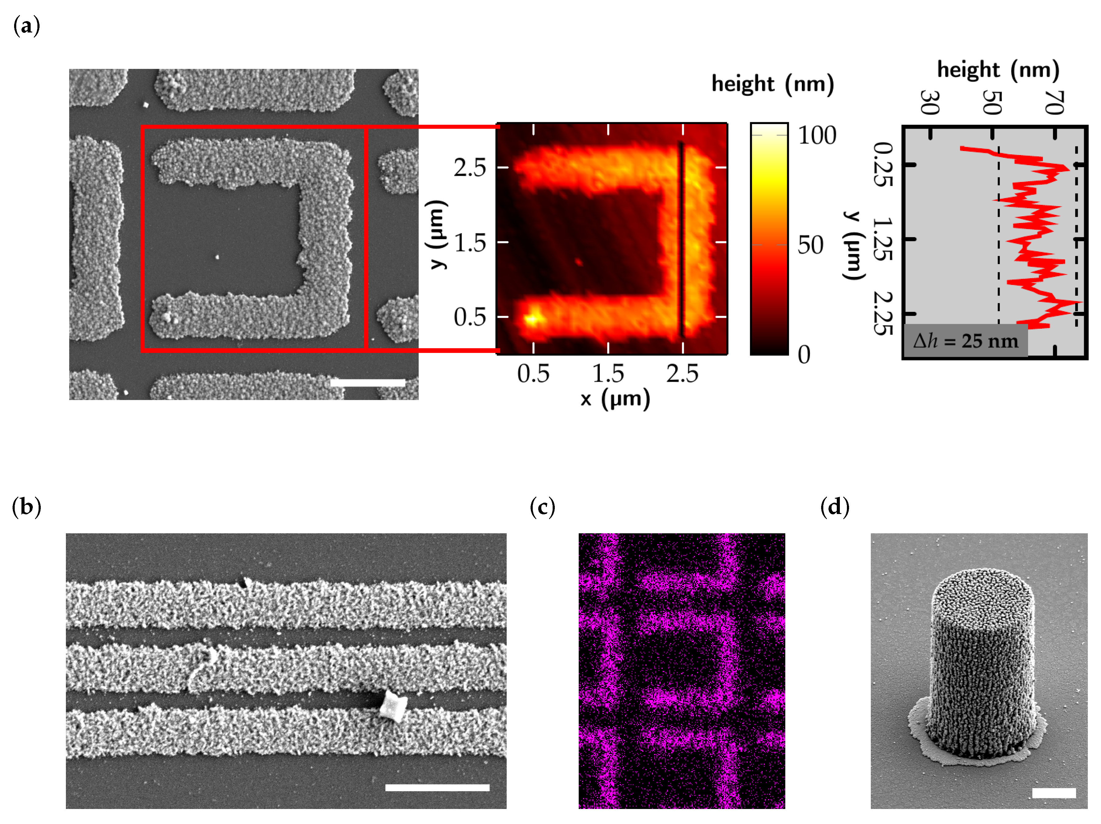
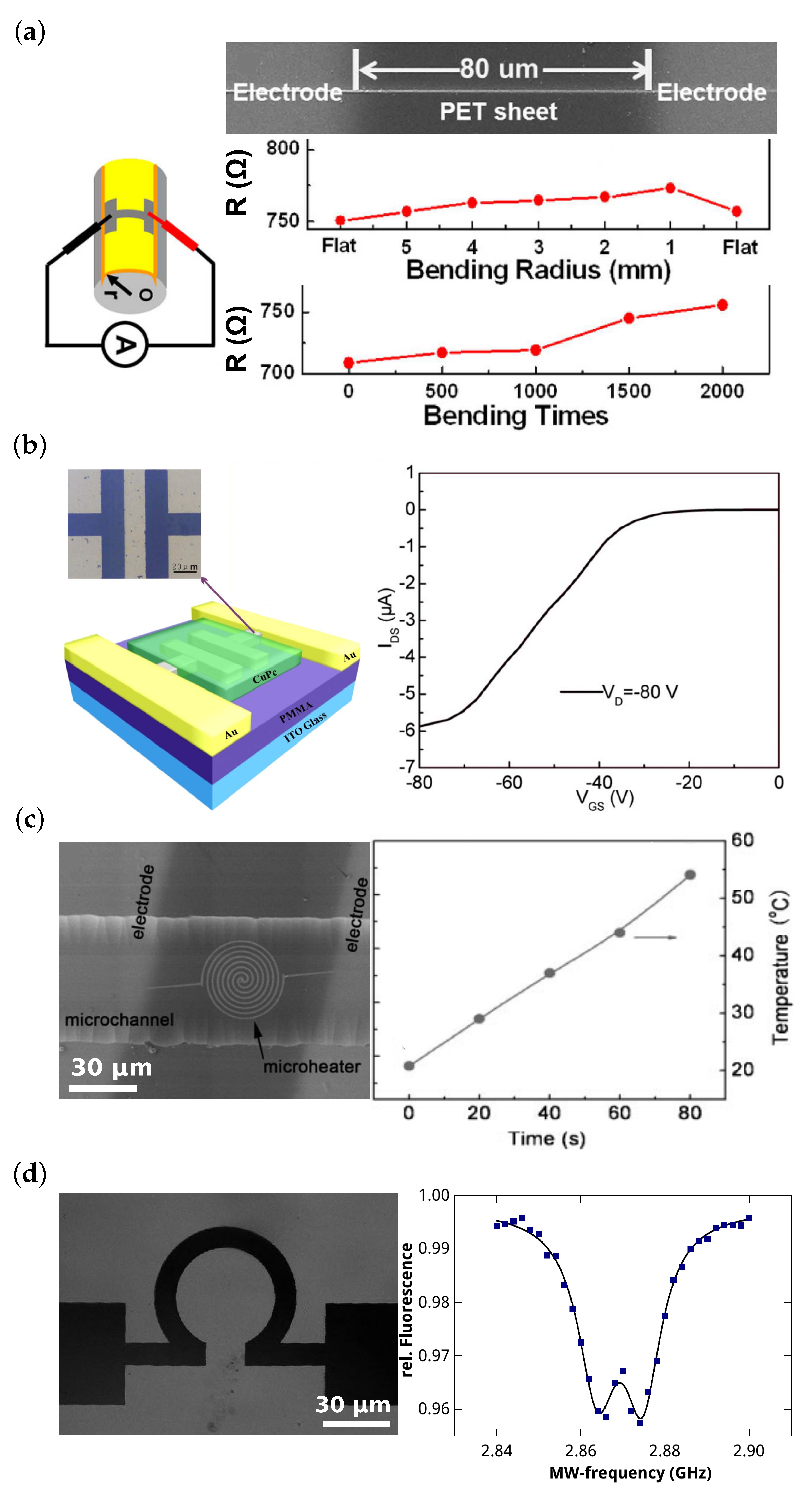
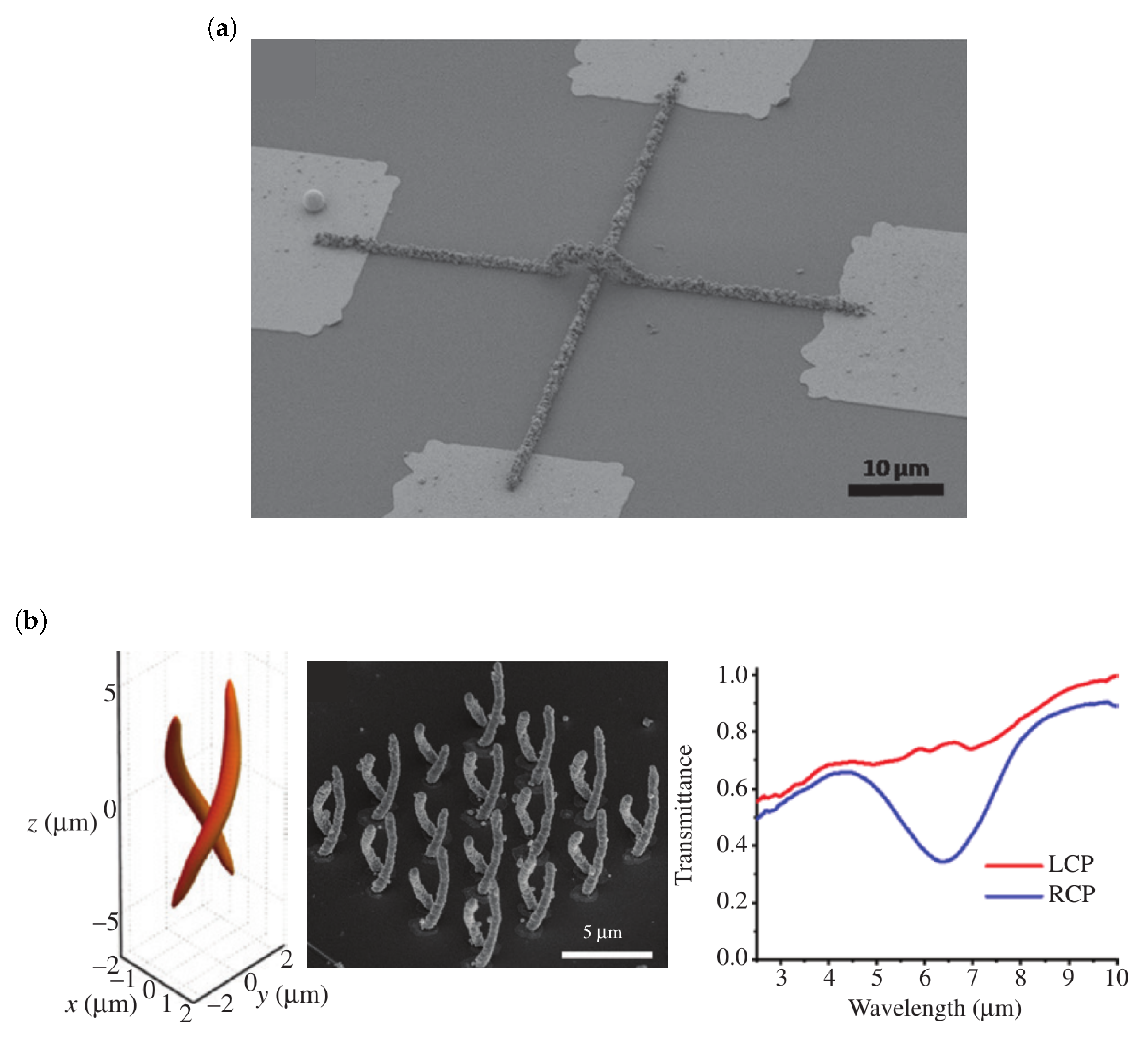
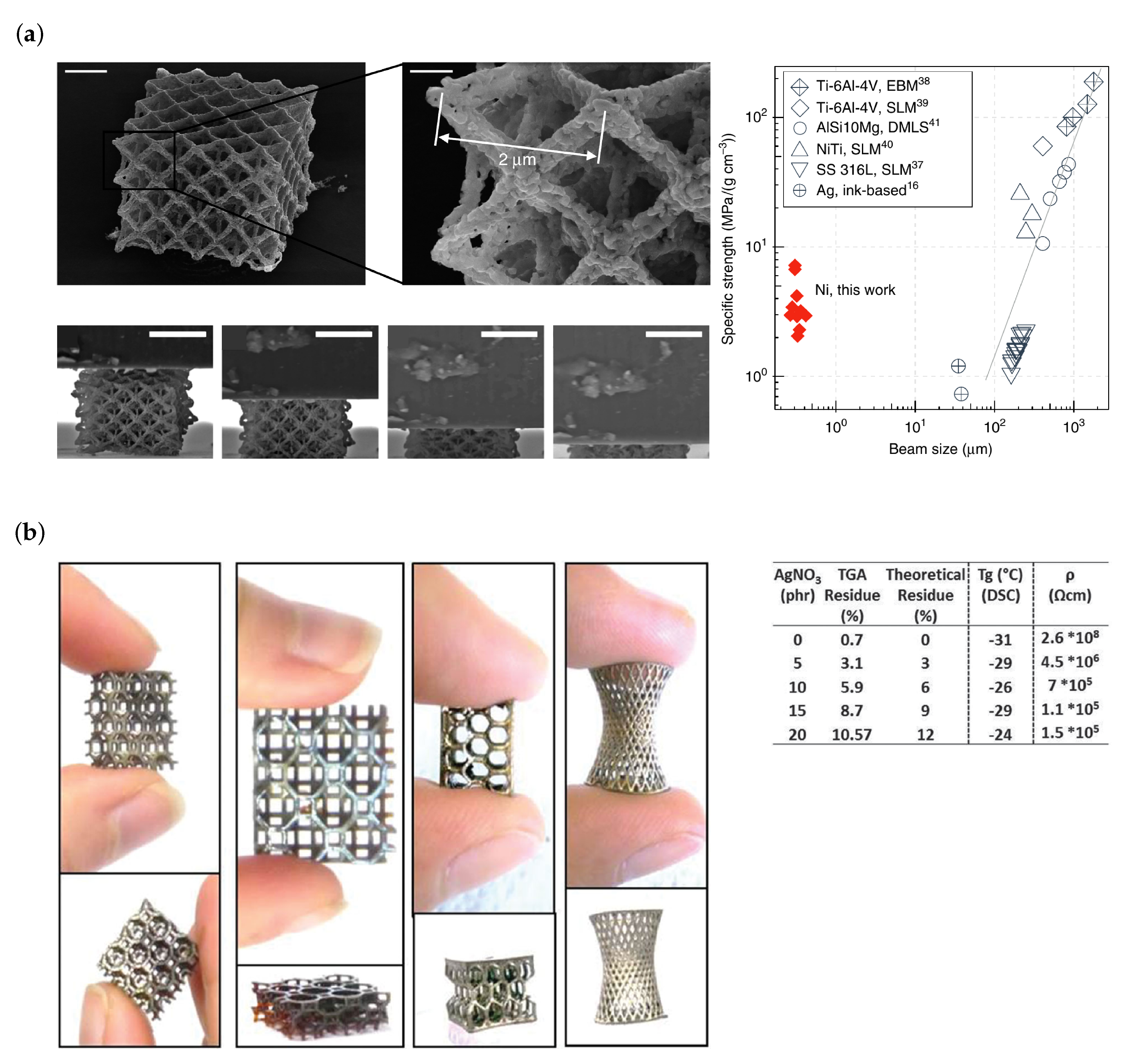
| Component Type | Material | Substrate | Resistivity | Dim. | Ref. |
|---|---|---|---|---|---|
| wires | Ag | flexible PET membrane | 2D | [46] | |
| OFET electrodes | Ag | PMMA | 2D | [47] | |
| microheater | Ag | non-planar microchannel | 2.5D | [48] | |
| GHz antenna | Ag | glass | 2D | own work | |
| (previously unpublished) | |||||
| gas sensor | Au-PVP- | microchannel | - | 2D | [52] |
| composite | |||||
| force sensor | Ag-PDMS- | glass, gold electrodes | 2D | [53] | |
| composite | |||||
| metamaterial | Ag | quarz | 2D | [54] | |
| metamaterial | Au | glass | 2D | [55] | |
| metamaterial | Ag | glass | ? | 2D | [56] |
| metamaterial | Au-SU8- | glass | - | 2D | [57] |
| composite | |||||
| metamaterial | Ag | glass | 2D | own work | |
| (previously unpublished) | |||||
| wires | Au-PEG- | glass | 3D | [58] | |
| composite | (after annealing) | ||||
| metamaterial | Ag | glass | 3D | [59] | |
| nanolattice | Ni | glass | - | 3D | [60] |
| microlattice | Ag-PEGDA- | glass | 3D | [61] | |
| composite |
© 2019 by the authors. Licensee MDPI, Basel, Switzerland. This article is an open access article distributed under the terms and conditions of the Creative Commons Attribution (CC BY) license (http://creativecommons.org/licenses/by/4.0/).
Share and Cite
Waller, E.H.; Dix, S.; Gutsche, J.; Widera, A.; von Freymann, G. Functional Metallic Microcomponents via Liquid-Phase Multiphoton Direct Laser Writing: A Review. Micromachines 2019, 10, 827. https://doi.org/10.3390/mi10120827
Waller EH, Dix S, Gutsche J, Widera A, von Freymann G. Functional Metallic Microcomponents via Liquid-Phase Multiphoton Direct Laser Writing: A Review. Micromachines. 2019; 10(12):827. https://doi.org/10.3390/mi10120827
Chicago/Turabian StyleWaller, Erik Hagen, Stefan Dix, Jonas Gutsche, Artur Widera, and Georg von Freymann. 2019. "Functional Metallic Microcomponents via Liquid-Phase Multiphoton Direct Laser Writing: A Review" Micromachines 10, no. 12: 827. https://doi.org/10.3390/mi10120827
APA StyleWaller, E. H., Dix, S., Gutsche, J., Widera, A., & von Freymann, G. (2019). Functional Metallic Microcomponents via Liquid-Phase Multiphoton Direct Laser Writing: A Review. Micromachines, 10(12), 827. https://doi.org/10.3390/mi10120827