A Smart Floating Gate Transistor with Two Control Gates for Active Noise Control


Abstract
1. Introduction
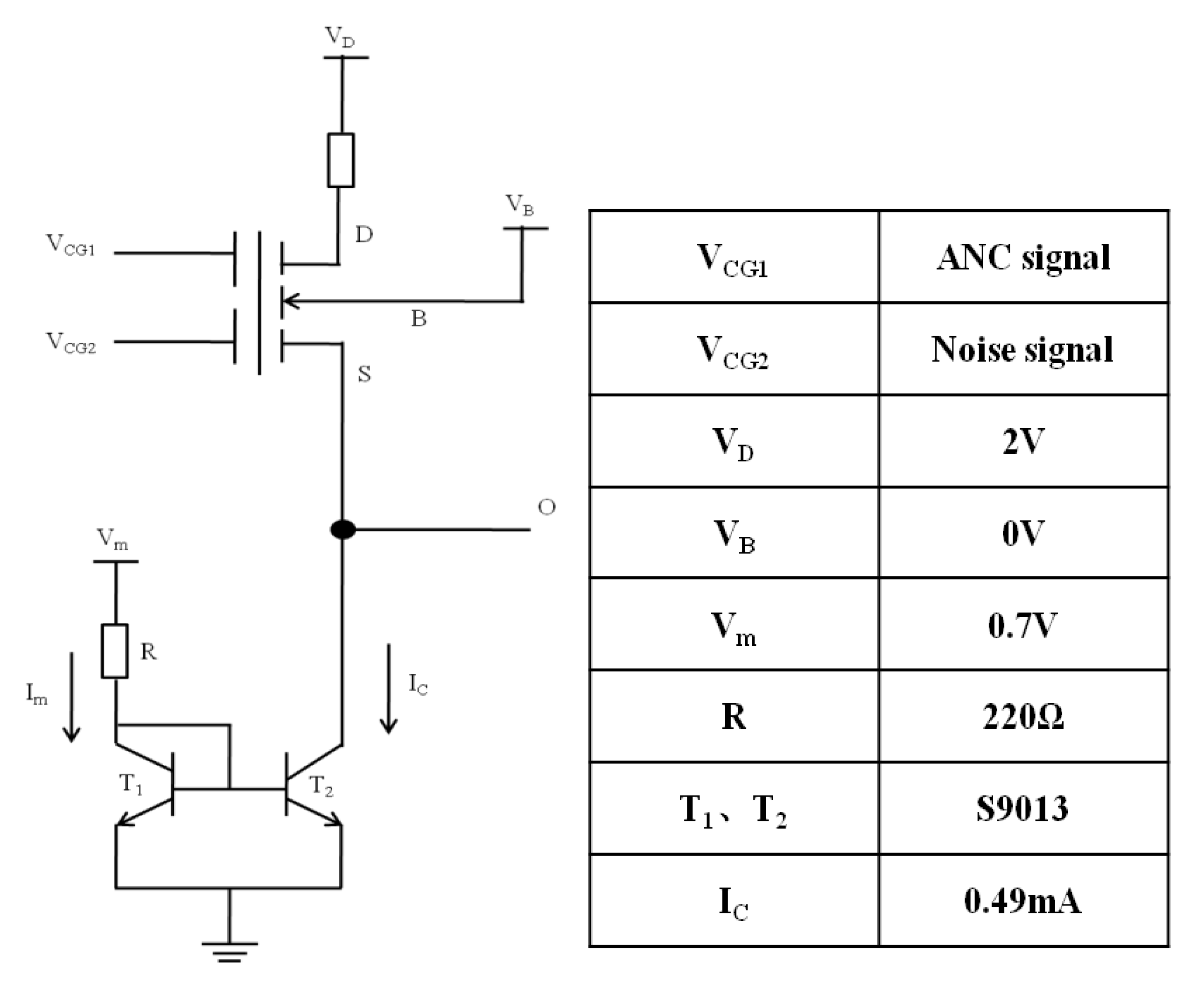
2. ANC Device
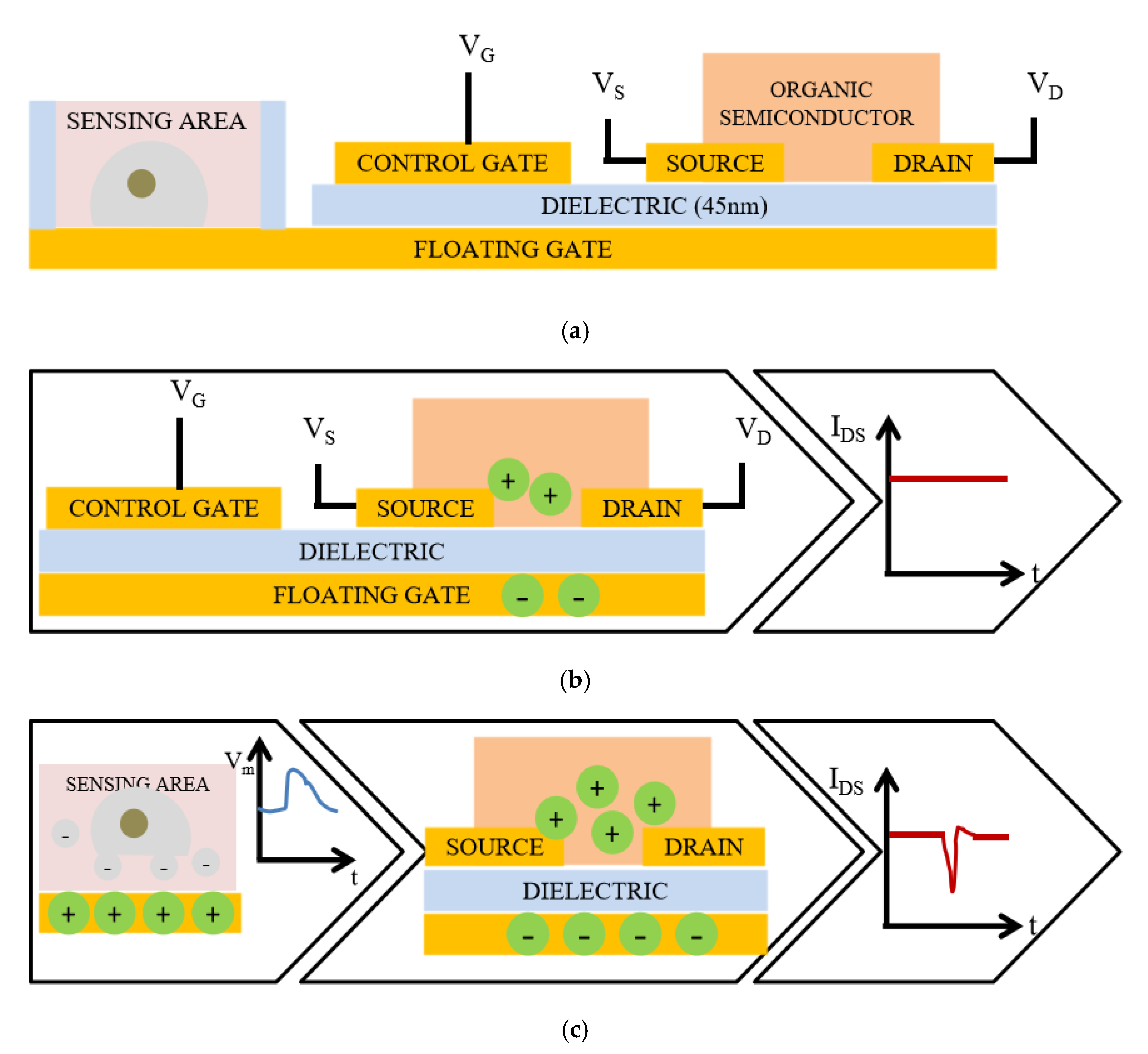
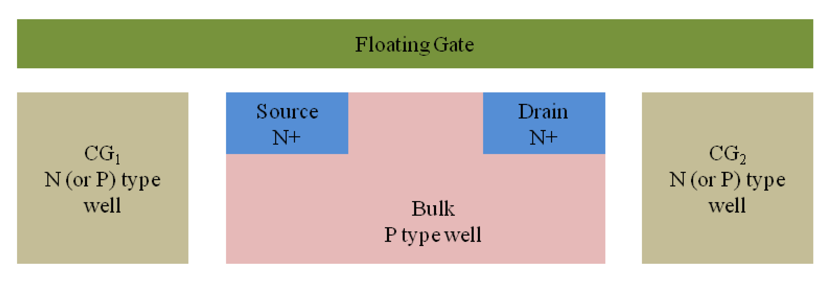
2.1. Device Structure
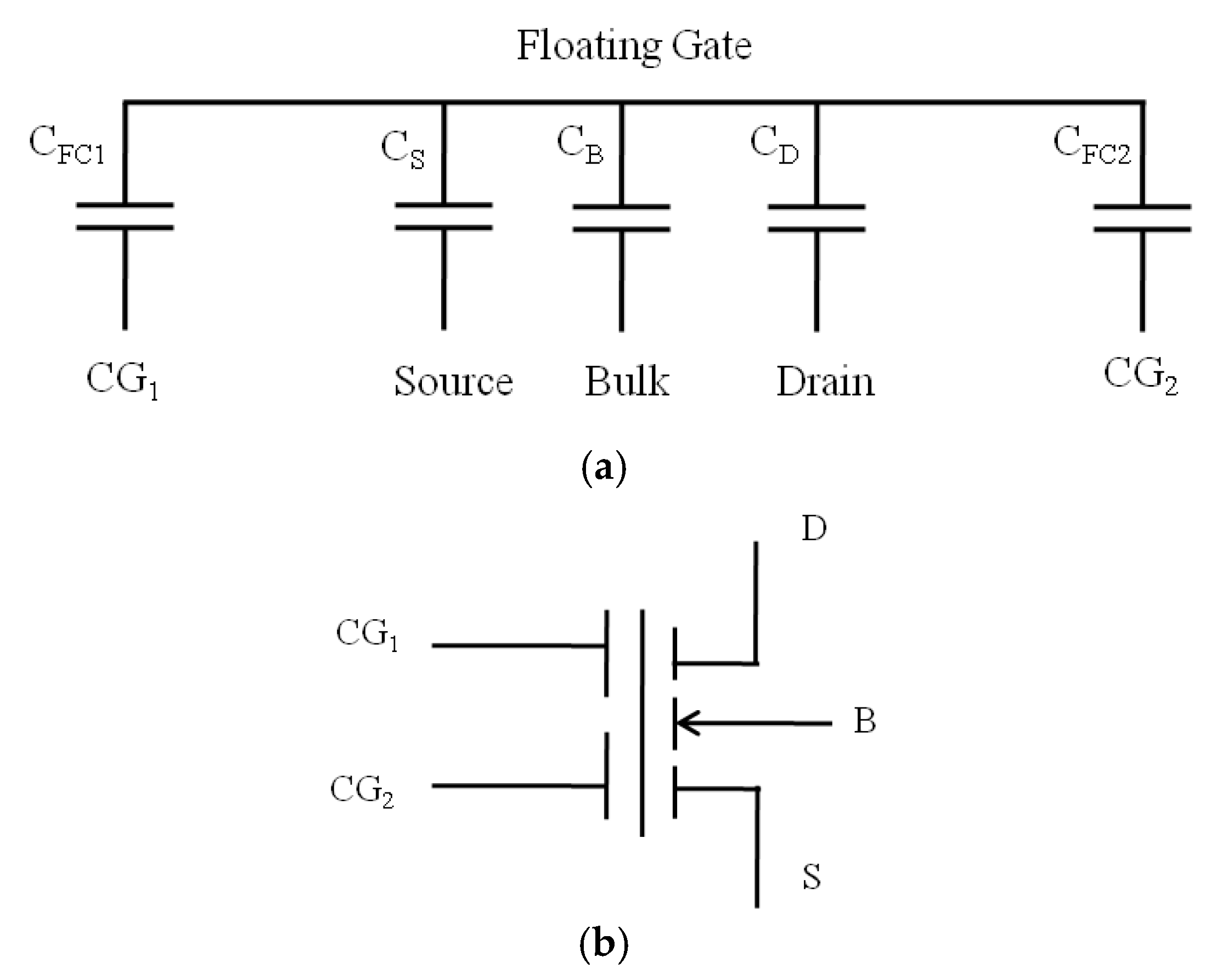
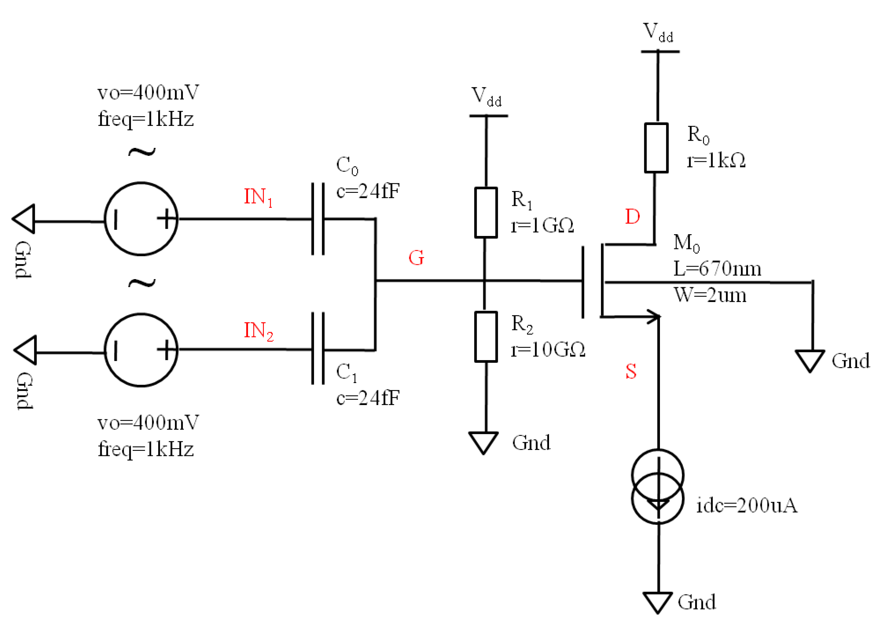
2.2. Device Model
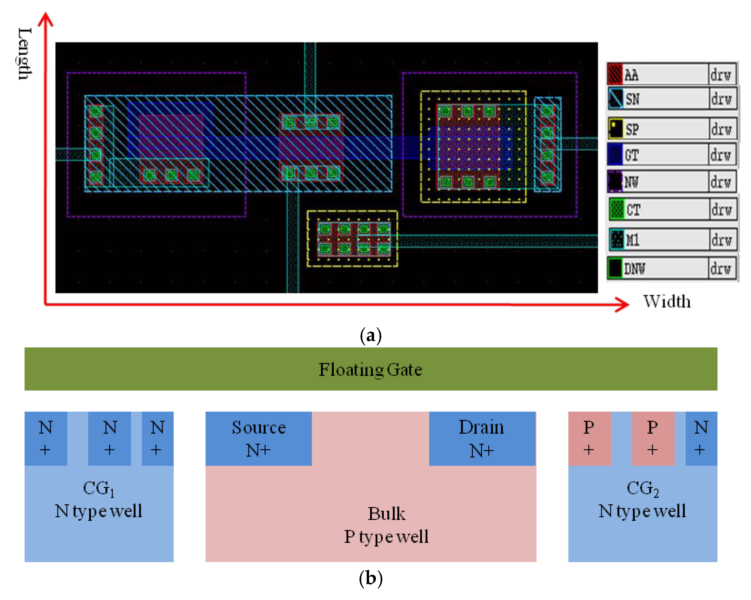
2.3. Device Layout
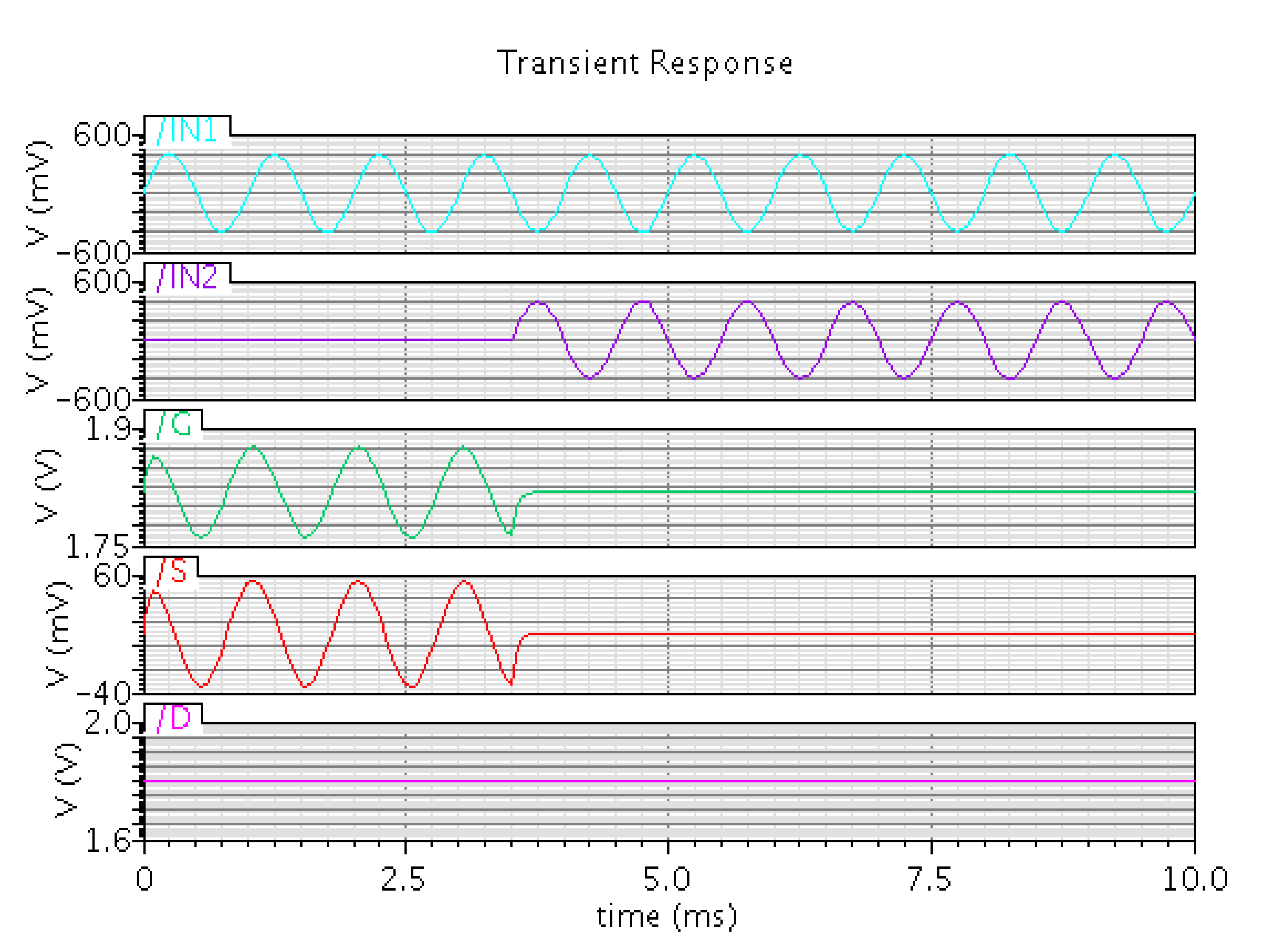
3. Simulation Results
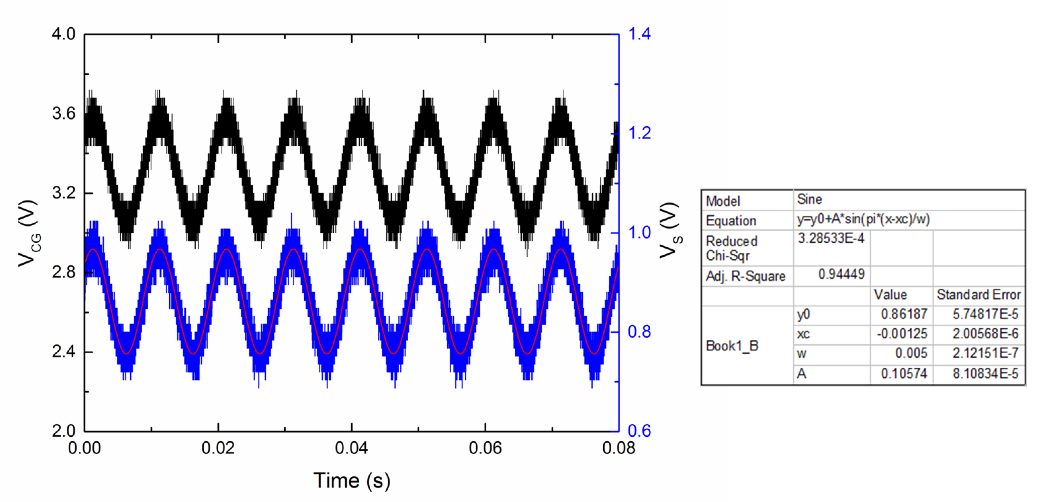
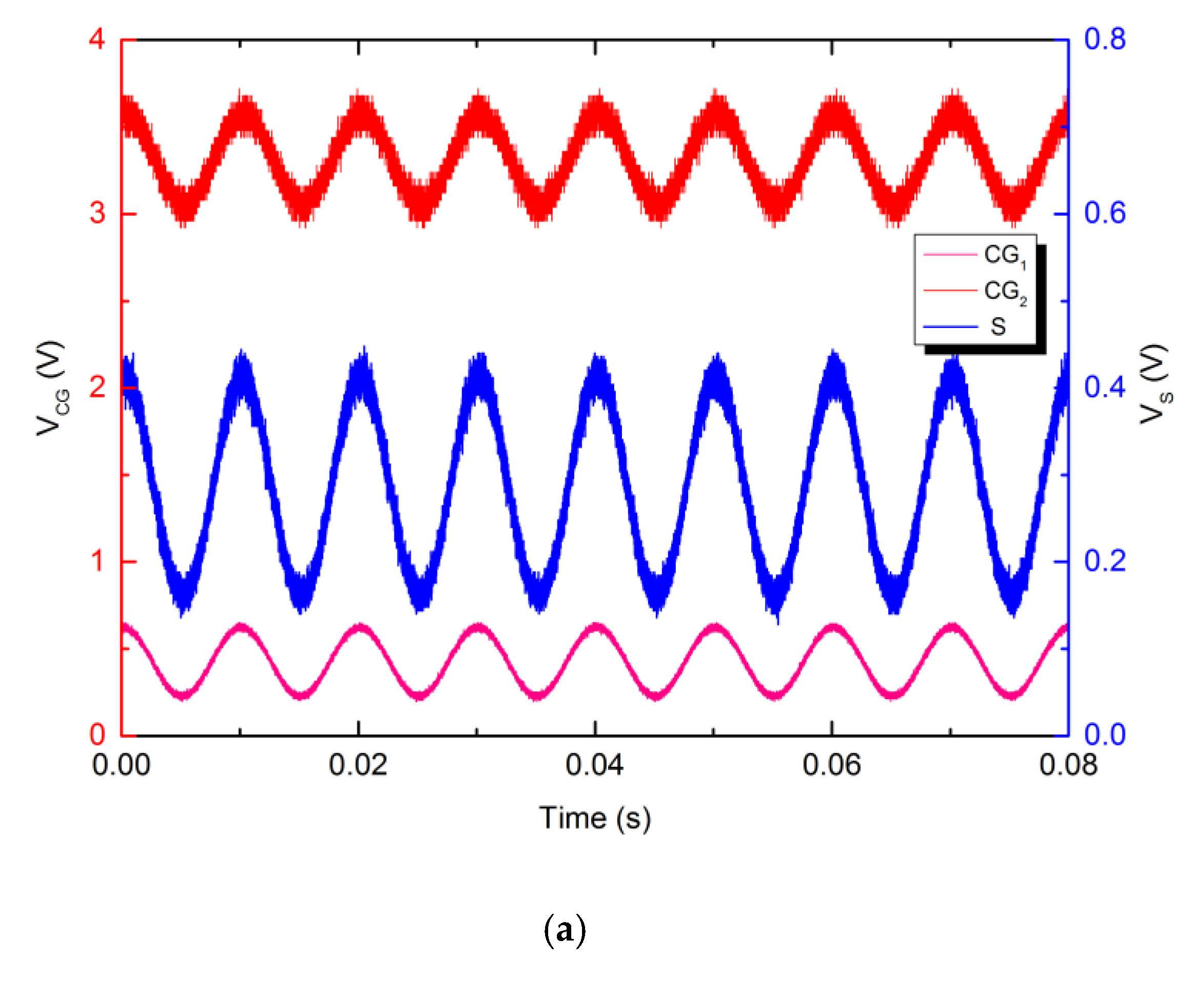
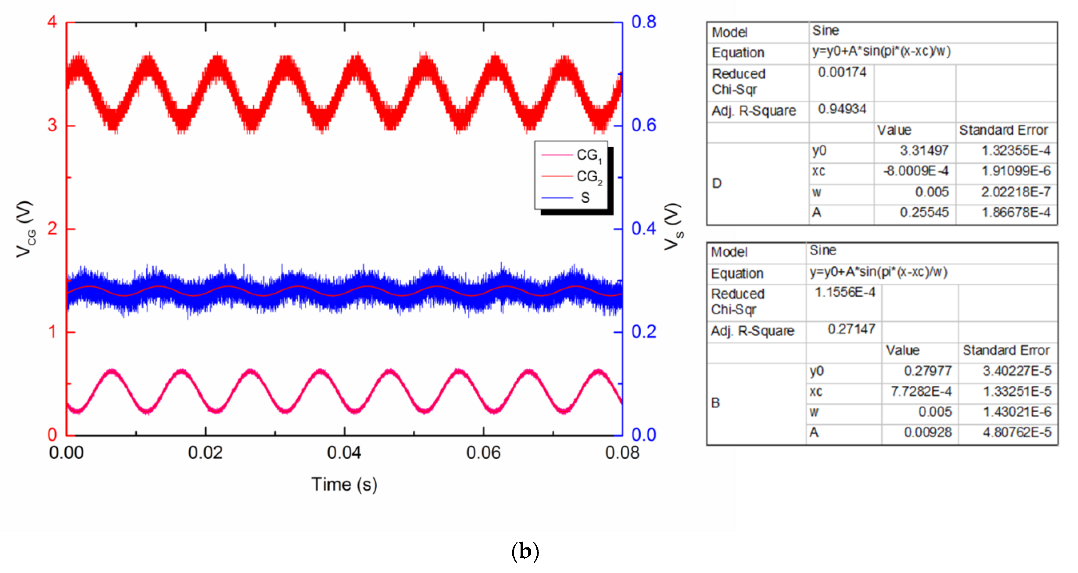
4. Experimental Results
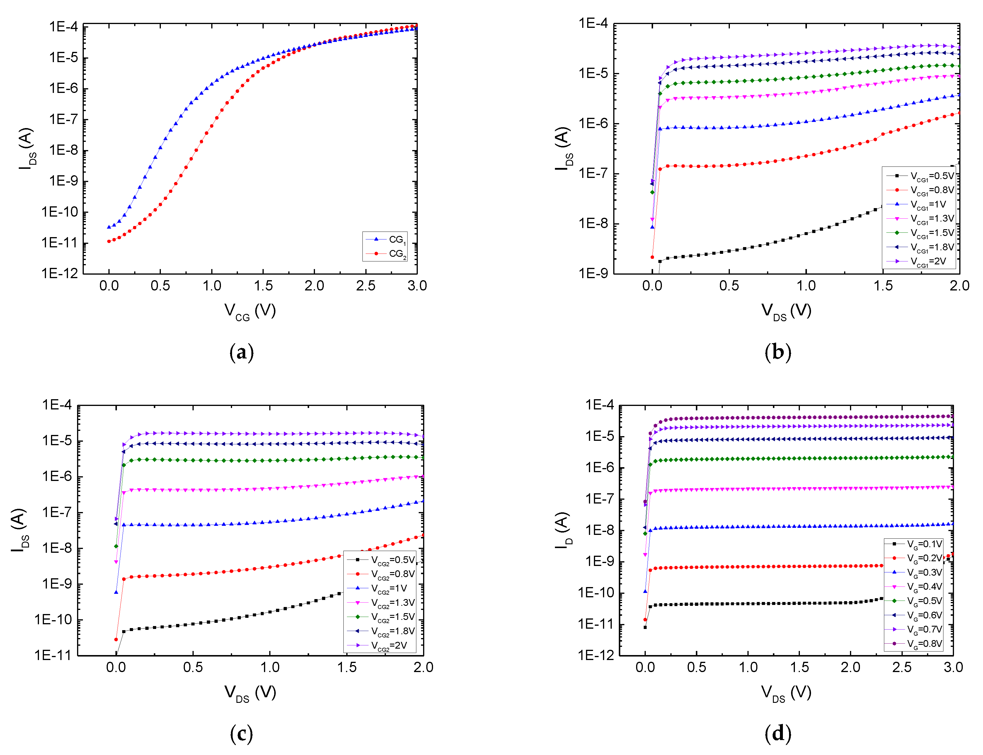
4.1. I–V Characteristics
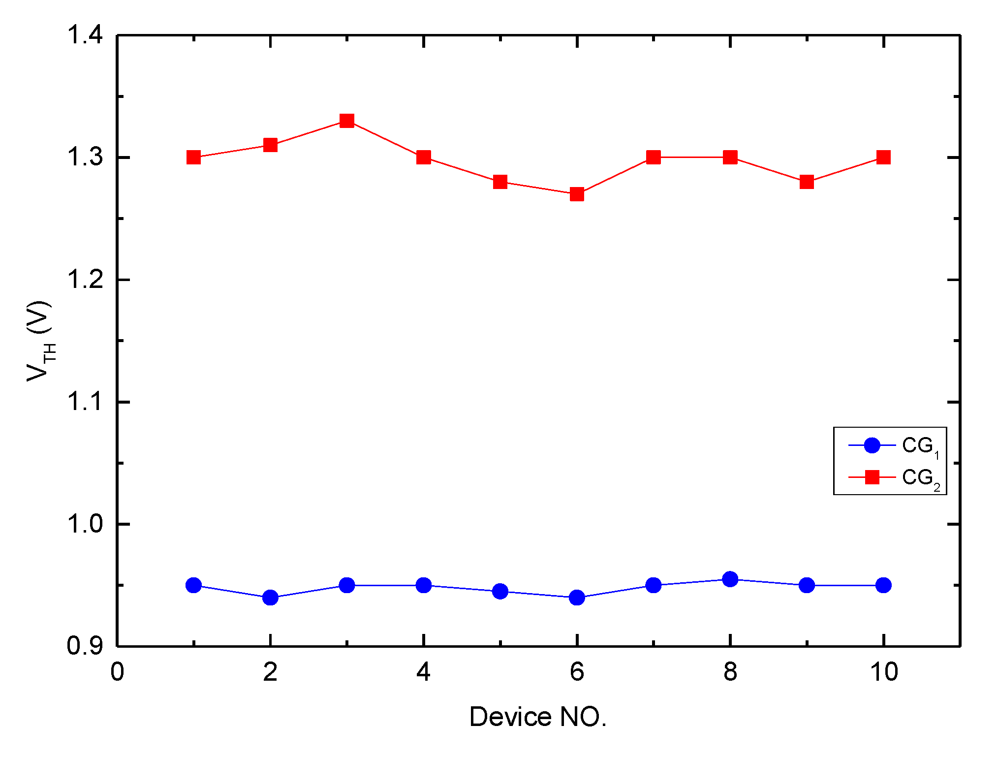
4.2. Device Threshold Characteristic
4.3. ANC Experimental Verification
5. Conclusions
Author Contributions
Funding
Conflicts of Interest
References
- Barbaro, M.; Bonfiglio, A.; Raffo, L. A charge-modulated FET for detection of biomolecular processes: conception, modeling, and simulation. IEEE Trans. Electron Devices 2006, 53, 158–166. [Google Scholar] [CrossRef]
- Meyburg, S.; Stockmann, R.; Moers, J.; Offenhäusser, A.; Ingebrandt, S. Advanced CMOS process for floating gate field-effect transistors in bioelectronic applications. Sens. Actuator B-Chem. 2007, 128, 208–217. [Google Scholar] [CrossRef]
- Zhang, Q.; Subramanian, V. DNA hybridization detection with organic thin film transistors: Toward fast and disposable DNA microarray chips. Biosens. Bioelectron. 2007, 22, 3182–3187. [Google Scholar] [CrossRef]
- Zhang, X.H.; Lee, S.M.; Domercq, B.; Kippelen, B. Transparent organic field-effect transistors with polymeric source and drain electrodes fabricated by inkjet printing. Appl. Phys. Lett. 2008, 92, 243307. [Google Scholar] [CrossRef]
- Kergoat, L.; Piro, B.; Berggren, M.; Pham, M.C.; Yassar, A.; Horowitz, G. DNA detection with a water-gated organic field-effect transistor. Org. Electron. 2012, 13, 1–6. [Google Scholar] [CrossRef]
- Jimenez-Jorquera, C.; Orozco, J.; Baldi, A. ISFET Based Microsensors for Environmental Monitoring. Sensors 2009, 10, 61–83. [Google Scholar] [CrossRef] [PubMed]
- Moser, N.; Rodriguez-Manzano, J.; Lande, T.S.; Georgiou, P. A Scalable ISFET Sensing and Memory Array with Sensor Auto-Calibration for On-Chip Real-Time DNA Detection. IEEE Trans. Biomed. Circuits Syst. 2018, 12, 390–401. [Google Scholar] [CrossRef] [PubMed]
- Ogier, S.D.; Matsui, H.; Feng, L.; Simms, M.; Mashayekhi, M.; Carrabina, J.; Terés, L.; Tokito, S. Uniform, high performance, solution processed organic thin-film transistors integrated in 1 MHz frequency ring oscillators. Org. Electron. 2018, 54, 40–47. [Google Scholar] [CrossRef]
- Krammer, M.; Borchert, J.W.; Petritz, A.; Karner-Petritz, E.; Schider, G.; Stadlober, B.; Klauk, H.; Zojer, K. Critical Evaluation of Organic Thin-Film Transistor Models. Crystals 2019, 9, 85. [Google Scholar] [CrossRef]
- Liao, C.; Yan, F. Organic Semiconductors in Organic Thin-Film Transistor-Based Chemical and Biological Sensors. Polym. Rev. 2013, 53, 352–406. [Google Scholar] [CrossRef]
- Lai, S.; Viola, F.; Cosseddu, P.; Bonfiglio, A. Floating Gate, Organic Field-Effect Transistor-Based Sensors towards Biomedical Applications Fabricated with Large-Area Processes over Flexible Substrates. Sensors 2018, 18, 688. [Google Scholar]
- Spanu, A.; Viola, F.; Lai, S.; Cosseddu, P.; Ricci, P.C.; Bonfiglio, A. A reference-less pH sensor based on an organic field effect transistor with tunable sensitivity. Org. Electron. 2017, 48, 188–193. [Google Scholar] [CrossRef]
- Demelas, M.; Lai, S.; Casula, G.; Scavetta, E.; Barbaro, M.; Bonfiglio, A. An organic, charge-modulated field effect transistor for DNA detection. Sens. Actuator B-Chem. 2012, 171–172, 198–203. [Google Scholar] [CrossRef]
- Lai, S.; Barbaro, M.; Bonfiglio, A. Tailoring the sensing performances of an OFET-based biosensor. Sens. Actuator B-Chem 2016, 233, 314–319. [Google Scholar] [CrossRef]
- Spanu, A.; Lai, S.; Cosseddu, P.; Tedesco, M.; Martinoia, S.; Bonfiglio, A. An organic transistor-based system for reference-less electrophysiological monitoring of excitable cells. Sci. Rep. 2015, 5, 8807. [Google Scholar] [CrossRef] [PubMed]
- Zhang, L.; Tao, J.; Qiu, X. Active control of transformer noise with an internally synthesized reference signal. J. Sound Vib. 2012, 331, 3466–3475. [Google Scholar] [CrossRef]
- Zhang, L.; Wu, L.; Qiu, X. An intuitive approach for feedback active noise controller design. Appl. Acoust. 2013, 74, 160–168. [Google Scholar] [CrossRef]
- Gan, W.S.; Mitra, S.; Kuo, S.M. Adaptive feedback active noise control headset: implementation, evaluation and its extensions. IEEE Trans. Consum. Electron. 2005, 51, 975–982. [Google Scholar] [CrossRef]
- Tseng, W.K.; Rafaely, B.; Elliott, S.J. Combined feedback–feedforward active control of sound in a room. J. Acoust. Soc. AM. 1998, 104, 3417–3425. [Google Scholar] [CrossRef]
- Pavan, P.; Bez, R.; Olivo, P.; Zanoni, E. Flash memory cells-an overview. Proc. IEEE 1997, 85, 1248–1271. [Google Scholar] [CrossRef]


| Device | Length (μm) | Width (μm) |
|---|---|---|
| CG1 | 1.375 | 2.01 |
| MOS | 0.67 | 2.03 |
| CG2 | 1.35 | 2.00 |
© 2019 by the authors. Licensee MDPI, Basel, Switzerland. This article is an open access article distributed under the terms and conditions of the Creative Commons Attribution (CC BY) license (http://creativecommons.org/licenses/by/4.0/).
Share and Cite
Mao, C.; Yang, C.; Ma, H.; Yan, F.; Zhang, L. A Smart Floating Gate Transistor with Two Control Gates for Active Noise Control. Micromachines 2019, 10, 722. https://doi.org/10.3390/mi10110722
Mao C, Yang C, Ma H, Yan F, Zhang L. A Smart Floating Gate Transistor with Two Control Gates for Active Noise Control. Micromachines. 2019; 10(11):722. https://doi.org/10.3390/mi10110722
Chicago/Turabian StyleMao, Cheng, Cheng Yang, Haowen Ma, Feng Yan, and Limin Zhang. 2019. "A Smart Floating Gate Transistor with Two Control Gates for Active Noise Control" Micromachines 10, no. 11: 722. https://doi.org/10.3390/mi10110722
APA StyleMao, C., Yang, C., Ma, H., Yan, F., & Zhang, L. (2019). A Smart Floating Gate Transistor with Two Control Gates for Active Noise Control. Micromachines, 10(11), 722. https://doi.org/10.3390/mi10110722