Article

Mathematical Modeling and Analysis of Capacitor Voltage Balancing for Power Converters with Fewer Switches

by
Mamdouh L. Alghaythi
1,*,
Gerald Christopher Raj Irudayaraj
2,
Senthil Kumar Ramu
3,*,
Praveenraj Govindaraj
2 and
Indragandhi Vairavasundaram
4
1
Department of Electrical Engineering, College of Engineering, Jouf University, Sakaka 72388, Saudi Arabia
2
Department of Electrical and Electronics Engineering, PSNA College of Engineering and Technology, Dindigul 624622, Tamilnadu, India
3
School of Electrical Engineering, Vellore Institute of Technology, Chennai 600127, Tamilnadu, India
4
School of Electrical Engineering, Vellore Institute of Technology, Vellore 632014, Tamilnadu, India
*
Authors to whom correspondence should be addressed.
Sustainability 2023, 15(13), 10698; https://doi.org/10.3390/su151310698
Submission received: 1 May 2023 / Revised: 21 June 2023 / Accepted: 29 June 2023 / Published: 7 July 2023

Abstract

:
The multilevel inverter (MLI) has been developed as a powerful power conversion scheme for several processes, including renewable energy, transmission systems, and electric drives. It has become popular across medium- to high-power operations due to its many advantages, including minimum harmonic content, low switching losses, and reduced electromagnetic interference (EMI). In this paper, the capacitor voltage balancing technique-based pulse width modulation (PWM) has been proposed. The proposed PWM strategy offers several advantages, such as high-quality output waveforms with reduced harmonic distortion, improved efficiency, and better control over the output voltage. The Xilinx ISE 10.1 software was used for synthesizing, and the VHDL code was written for the proposed method. MATLAB software was used to simulate and hardware was used to verify the proposed system. The SPARTAN 3E FPGA was used for the generation of the PWM. This paper developed a 2 kW single-phase 15-level inverter that created an AC wave from the DC input voltage, with a total harmonic distortion (THD) of 8.02%, which was less than the THD achieved from other conventional MLI. The results indicate that MLI topologies with low total harmonic currents, fewer switches, and higher output voltage levels are better stabilized during load disturbance circumstances.

1. Introduction

Global warming is a major environmental issue affecting the entire world. It refers to the gradual increase in the Earth’s average surface temperature caused by the buildup of greenhouse gases in the atmosphere. The primary cause of global warming is human activity, particularly burning fossil fuels for energy and transportation, deforestation, and industrial processes. The impacts of global warming are far-reaching and can be felt worldwide [1,2]. Reducing greenhouse gas emissions is the most efficient approach to address global warming. It can be achieved through various strategies, such as transitioning to clean and renewable energy sources, improving energy efficiency, promoting public transportation, and implementing policies to reduce emissions from industries and agriculture [3].
A solar PV system converts sunlight into electricity using solar panels. Solar PV systems are becoming increasingly popular as a clean and sustainable alternative to traditional energy sources. A typical solar PV system consists of solar panels, an inverter, and a battery bank (optional). Solar panels consist of photovoltaic cells that convert sunlight into DC. An inverter converts the DC to AC, which powers household appliances and electronics. This output is influenced by solar radiation and temperature and is not steady [4,5]. Therefore, it is important to obtain the most power possible out of solar PV, which is achieved by maximum power point tracking (MPPT) [6], for a PV panel to operate effectively even under numerous climatic changes throughout an annual calculation [7].
The use of an MPPT controller with this DC-to-DC converter offers several benefits. By ensuring that the solar panels operate at their maximum efficiency, the system can generate more energy, reducing the size of the solar panel array required to meet energy demands. Using a DC-to-DC converter also improves the system’s efficiency by reducing losses in the power conversion process. It can lead to a more cost-effective and reliable solar PV system.
Since they have been around for over 50 years, multilevel inverters (MLIs) are gaining popularity in industrial settings as one of the fascinating ways to deploy medium- to high-power converters. Multilevel inverters are an important technology in power electronics that have gained significant attention in recent years due to their potential to provide high voltage and power quality to various applications. A multilevel inverter consists of several power electronic switches arranged in a specific configuration to produce multiple output voltage levels. The configuration for MLI depends on the number of levels and clamping used to achieve these levels.
An analytical indication for improving the quality of the alternating voltage is provided by MLI topologies [8]. Over traditional two-level inverters, MLIs offer several benefits, including a greater basic voltage at the output, reduced typical mode voltage and switch loss, less EMI, and less THD. Power electronic applications are crucial for the multilayer inverter to convert a direct current source. Several issues exist with the three-phase alternating machine and system supply PWM signaling approaches [9]. Since low-level inverters contain nonlinear elements such as MOSFET and IGBT, they may also produce waveforms with harmonics using pulse-width modulation (PWM) [10]. Nonlinear impacts such as distortion caused by harmonics develop on the outputs of load when the amount of the element has risen on the inverter. Studies have considered nonlinear impacts to reduce the impact of harmonic distortion on the operating loads of PWM inverters [11].
The cascaded H-bridge MLI consists of a succession of H-bridge inverters connected in a cascaded configuration. Each H-bridge inverter has four switches (upper arm = 2 and lower arm = 2) that switch the voltage to produce the needed DC output voltage waveform. The number of levels for the inverter is determined by the number of H-bridge modules used [12]. Increasing the DC-link voltage results in greater electromagnetic interference and voltage stress on power semiconductor devices [13]. Topologies that employ multiple levels of inverters can decrease the voltage stress of switches and EMI in the system, thus replacing the two-level inverter [14]. The cascaded H-bridge MLI offers various benefits over conventional inverters, including reduced harmonic distortion, improved voltage quality, lower EMI, higher efficiency, and a modular design. These advantages make it well suited for various applications such as renewable energy systems, motor drives, and electric vehicles.
PWM technology removes and lowers harmonics at the inverter output while controlling the output voltage. PWM serves the dual purpose of reducing or eliminating harmonics and controlling the voltage inside the inverter without an additional hardware price. With developments in MLIs, innovative modulation methods are increasingly necessary for these devices. Each modulation approach has negative and positive influences on the converter architecture and scope. The categorization of the modulation schemes for MLIs based on the difference between high- and low-frequency shifting is represented in [15]. Level shifting and phase shifting modulation schemes are two categories of PWM systems based on the waveform. To create high-quality output voltage waveforms, level shift modulated methods are commonly used in many applications [16,17].
Capacitor voltage balance (CVB) represents one of the most important problems for MLIs due to the modular design. The two primary forms of capacitor-voltage-balancing methods are arm regulation [18] and specific capacitor regulation [19]. The first approach, which necessitates a closed-loop regulation for each capacitor, must be revised for MMCs with many capacitors. The latter is the sorting and selection (SAS) approach and uses all the capacitors in an arm. It sorts the capacitor voltages and chooses included or skipped sub-modules (SMs) by the signal of the arm current.
This PWM scheme provides periodic unneeded activation of the switches and supplies to turn up the initial level while producing a high-level voltage. The additional supply and switch action reduces the switch’s lifetime and results in power loss. A new fraction sinus PWM improvement with a gap is presented in [20] on a three-phase signal processing approach. The dual DC to DC converter featuring a reverse connection for the MLI is suggested [21]. Ref. [22] discusses investigating the primary PWM operation instances and frequencies that influence this zero-crossing point.
An MLI with the fewest possible power electronic switching elements was proposed in this study. It used a multilayer inverter created in [23,24] and modified somewhat. By utilizing the inverter’s series/parallel switches, the proposed MLI introduced an auxiliary network with four diodes and a toggle switch. In contrast to the traditional cascaded H-bridge inverters, just two independent source voltages were required to generate an equal number of voltage levels. Compared with existing techniques, the proposed inverter used fewer switching elements and had lower harmonics in the output voltage waveforms. The applicability of grid-tied photovoltaic systems, hybrid electric cars, etc., could be expanded using the proposed MLI design. In this proposed system, the RL load was considered from the inverter with the values of 100 Ω and 30 mH, respectively, for 11 and 15 levels of the inverter. In addition, the bottom and top inverter voltages for 11 levels were 65 V and 130 V, and those for 15 levels were 47 V and 94 V. Mathematical analyses, computer simulations, and experimental findings are provided to prove the proposed cascaded MLI’s viability.
The field programmable gate arrays (FPGAs) used to implement various PWM regulators have grown progressively over the past few years. Because of their flexibility compared with other digital signal processors (DSPs), they are becoming the leading devices for employing various PWMs.
The main objective of this paper is to develop a CVB-based PWM technique for 11- and 15-level inverters. This investigation offers a new MLI design that uses two DC sources and eight power electronic components to generate 11 and 15 levels. Based on the measured findings, the proposed MLI offers high-quality, consistent output waveforms with a decreased THD. In hardware, PWM generation was carried out using SPARTAN 3 A FPGA kit.
The paper’s structure is as follows: Section 2 presents the cascaded H-bridge MLI that is being proposed. Section 3 discusses the problems with the proposed inverter’s capacitor voltage balancing. Section 4 illustrates the PWM pulse modeling for the proposed cascaded MLI. In Section 5, the outcomes of the proposed system are analyzed. Furthermore, Section 6 provides an overview of the conclusions drawn from this paper.

2. Proposed Cascaded H-Bridge MLI

The proposed inverter had a top and bottom inverter in which the top inverter’s primary switches were triggered with high frequency, while the bottom inverter was triggered with low frequency, as shown in Figure 1. The top three-level inverter had four switches with output levels of 0, +Vdc, and −Vdc. The bottom inverter had four basic primary switches and a second bidirectional switch, which could be increased to increase the overall level of the inverter.

2.1. Modes of Operation

Figure 2 illustrates the suggested bottom inverter’s operating modes, comprising four IGBT switches and two bidirectional switches. The green color indicates the conduction of switches and capacitors [25].
Switching mode 1, depicted in Figure 2a, involved turning on switches PS5 and PS6 while turning off the remaining switches. This configuration produced a voltage output of 0 [26].
The system had seven different switching modes.
In switching mode 1, switches PS5 and PS6 were on, while the others were off, producing a voltage of 0 (Figure 2a).
In switching mode 1, switches PS7 and PS8 were on, while the others were off, producing a voltage of 0 (Figure 2b).
Switching mode 2 involved switches PS8 and SS2 being on and the others being off, resulting in a voltage of 2 Vdc0 (Figure 2c).
Switching mode 3 entailed turning on switches PS8 and SS1 while keeping the others off, generating a voltage of 4 Vdc0 (Figure 2d).
In switching mode 4, switches PS5 and PS8 were on, and the rest were off, yielding a voltage of 6 Vdc0 (Figure 2e).
In switching mode 5, switches PS6 and SS1 were on, while the others were off, producing a voltage of −2 Vdc0 (Figure 2f).
Switching mode 6 involved switches PS6 and SS2 being on and the others being off, resulting in a voltage of −4 Vdc0 (Figure 2g).
Finally, in switching mode 7, switches PS6 and PS7 were on, while the rest were off, generating a voltage of −6 Vdc0 (Figure 2h).
The various modes of operation of the proposed MLI are represented in Figure 2. The switching modes of the H-bridge inverter are illustrated in Table 1. It describes various active and non-active modes of IGBT switches.
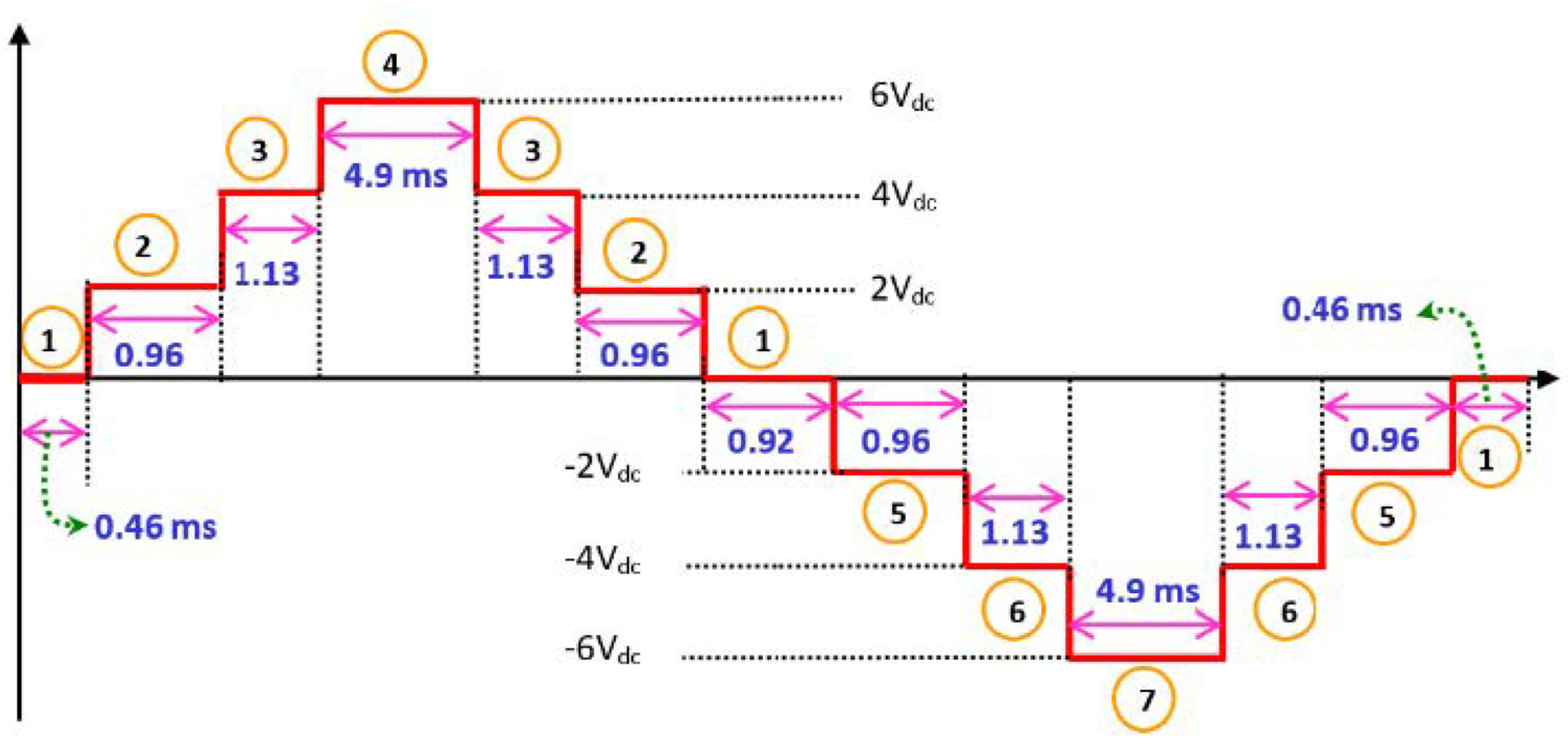
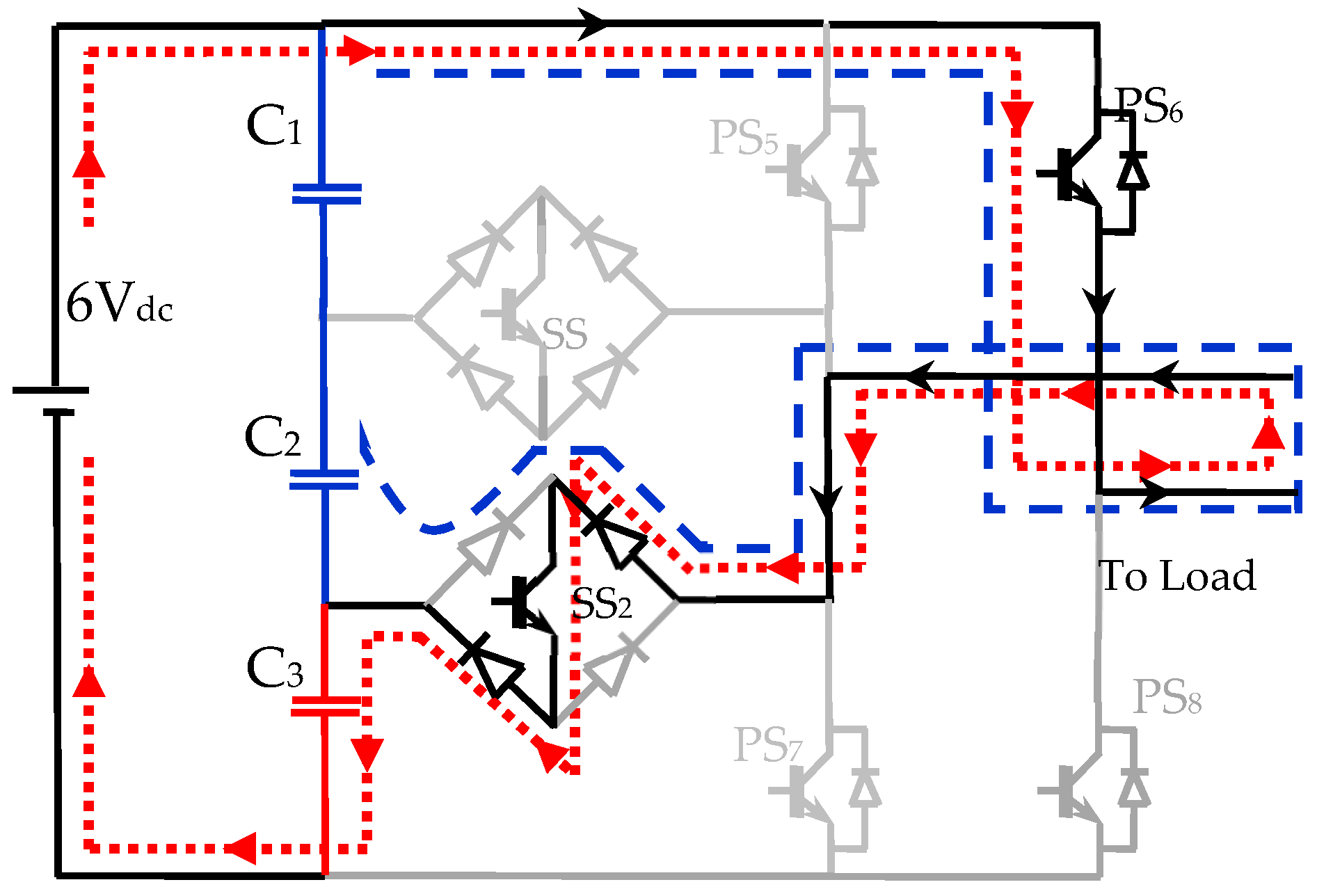
To maintain a frequency of 50 Hz over a total period of 0.02 s, Figure 3 displays the projected seven-stage output of the suggested bottom inverter. Figure 4, Figure 5, Figure 6 and Figure 7 display the direction of current flow during the charging and discharging cycles of capacitors C1, C2, and C3. The dotted line indicates the charging phase, while the dashed line represents the discharging phase of the capacitors [26,27].

2.2. Capacitor States of Bottom H Bridge Inverter

During mode 2, capacitors C1 and C2 were charged, and capacitors C3 discharged. Similarly, in mode 3, capacitor C1 charged, while capacitors C2 and C3 discharged, as depicted in Figure 5. During mode 5, capacitor C1 discharged, whereas capacitors C2 and C3 charged.
Likewise, during mode 6, C1 and C2 discharged, whereas C3 charged. Table 2 provides a detailed account of each capacitor’s charging and discharging duration [28].
From Table 2, it is concluded that
  • C1 and C3 total charging time = 4.18 milli seconds;
  • C1 and C3 total discharging time = 4.18 milli seconds;
  • C2 total charging time = 3.84 milli seconds;
  • C2 total discharging time = 4.52 milli seconds.
The capacitor charging and discharging times should typically be equal to be balanced. According to the information above, capacitors C1 and C3 had equal charging and discharging times for cycles of 20 ms and were, therefore, balanced. However, capacitor C2 did not have an equal charging and discharging time and needed to be balanced. So, the solution for this problem, the capacitor balancing process, was required in this proposed seven-level inverter’s charging and discharging duration [28].

3. Capacitor Voltage Balancing in the Proposed Inverter

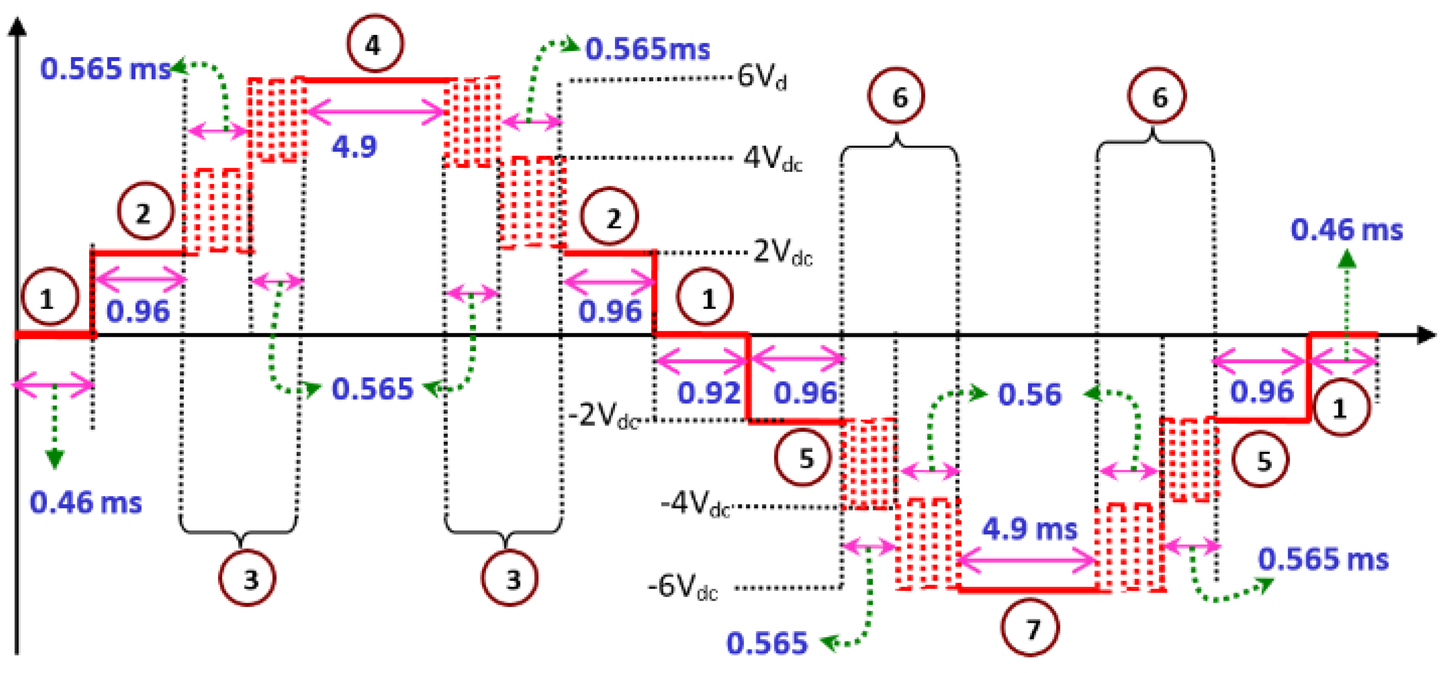
The seven-level inverter was proposed to eliminate the capacitor voltage balancing problem in capacitor C2. Thus, the total voltage in the capacitor over 20 ms became positive [16]. It could be implemented during modes 3 and 6, where the capacitor C2 voltage decreased. Figure 8 shows the proposed capacitor voltage balancing technique, a modified switching technique. During switching stages 3 and 5, it was apparent that the proposed inverter voltage may switch among two levels.
During mode 3, the inverter voltage was shifted among 2 Vdc and 4 Vdc for the first part of the time interval and among 4 Vdc and 6 Vdc during the next part of the time interval. This reduced the discharging time of C2 in mode 3. Because of this switching, the voltage was either in 2 Vdc or 6 Vdc, increasing the charging time of capacitor C2. The cascaded output of the top- and bottom-level inverter is shown in Figure 9. The low switching frequency inverter (LSFI) and high switching frequency inverter (HSFI) voltages were immediately coupled to produce the load voltage. It can also be seen in Figure 9 (the magnified area) that at switching state 3 of the lower inverter, the HSFI should flip in the opposite direction of the LSFI. This was critical for switching the load voltage among 4 Vdc and 5 Vdc, as well as 5 Vdc and 6 Vdc. C2 will begin charging in addition to C1 and C3 if the changed switching architecture powers the proposed inverter. As a result, the voltage over C2 must be monitored, and depending on its current value, either the generalized reduced switching method or the altered modulation strategy must be employed.

4. Modeling of PWM Pulses for Proposed Cascaded Multilevel Inverter

To produce the reference waveform for the top inverter, the following Equations (1) and (2) were utilized [17]:
U r e f = A sin ω t
U r e f , s = U r e f 7
Z 1 = 1   if   U r e f > 0 0   if   U r e f < 0
V b o t t o m , e x p e c t e d = r o u n d U r e f , s 0.4 * 0.4 * Z 1 + r o u n d U r e f , s 0.4 * 0.4 * Z 1
V t o p , r e f = 7 * U r e f , s V b o t t o m , e x p e c t e d
Equation (3) describes the zero-crossing detector, while Equation (4) represents the projected output of the bottom inverter (Vbottom). Equation (5) provides a mathematical expression for the reference waveform of the top inverter. The following equations must construct and describe the reference waveform to provide the PWM for the bottom inverter:
V b o t t o m , r e f = r o u n d U r e f , S 0.4
After generating the reference waveform, it was divided into various waves Ry.
X = N 11 4 + 2
where N = 11, 15, 19, 23
R y = 1   if   U b o t t o m , r e f > y 0   if   U b o t t o m , r e f < y
The total number of secondary switches required for an N-level inverter was determined after dividing by the number of different signals.
N A S = N 11 4 + 12
where N = 11, 15, 19, 23 …
The turn-on and turn-off operation of the primary switches (PSs) of the bottom inverter was determined by the following equations:
P S 5 t = R 1 ¯ + R y ¯ * Z 1
P S 6 t = R 1 + Z 1 ¯ + R 1 ¯ * Z 1
P S 7 t = R 1 ¯ + R y * Z 1
P S 8 t = R 1 + Z 1 + R 1 ¯ * Z 1 ¯
where y = X, + stands for logical OR, and * stands for multiplication. The following expression determines how the bottom inverter’s secondary switches operate when they are turned on and off:
Step 1.
Form a set:
R = R 1 , R 2 , R 3 , R 4 , .. R y 3 , R y 2 , R y 1 , R y
Step 2.
Write the permutation P on R :
P = R 1 R 2 R 3 R y 2 R y 1 R y R 2 R 3 R 4 R y 1 R y R 1
Step 3.
Eliminate the final column in the above permutation P1 and rework as
P 1 = R 1 R 2 R 3 R y 3 R y 2 R y 1 R 2 R 3 R 4 R y 2 R y 1 R 1
Step 4.
We can develop the switching signals for the secondary switches calculated from the above equation. The first and last columns of the matrix are responsible for establishing the switching patterns for the initial and final secondary switches, respectively. The equations for SS1 and SSn are also included.
S S 1 t = R 1 R 2 * Z 1 ¯ + R y 1 R y * Z 1
S S n t = R 1 R 2 * Z 1 + R y 1 R y * Z 1 ¯
where the XOR (exclusive OR) operation is represented as . In a similar manner, the second column of the permutation matrix P1 was used to generate the switching patterns for SS2, while the second column from the end was used for SS(n−1). The expressions were as follows:
S S 2 t = R 2 R 3 * Z 1 ¯ + R y 2 R y 1 * Z 1
S S n 1 t = R 2 R 3 * Z 1 + R y 2 R y 1 * Z 1 ¯
The switching states and expected output of the proposed fifteen-level inverter are represented in Table 3. It shows the top and bottom H-bridge switches in an active and non-active mode. The primary switches PS1 and PS3 were turned on and off by comparing the MR01 reference waveform with the triangular carrier wave, and PS2 and PS4 were turned on and off by comparing the MR02 reference waveform with the triangular carrier wave, as shown in Figure 10. The resulting voltage Vyz was obtained from the waveform. The primary switches of the lower inverter from PS5 to PS8 were turned on and off concerning Equations (10)–(13), and the secondary switches SS1 and SS2 were turned on and off regarding Equations (17)–(19) as represented in the switching signals.

5. Results and Discussion

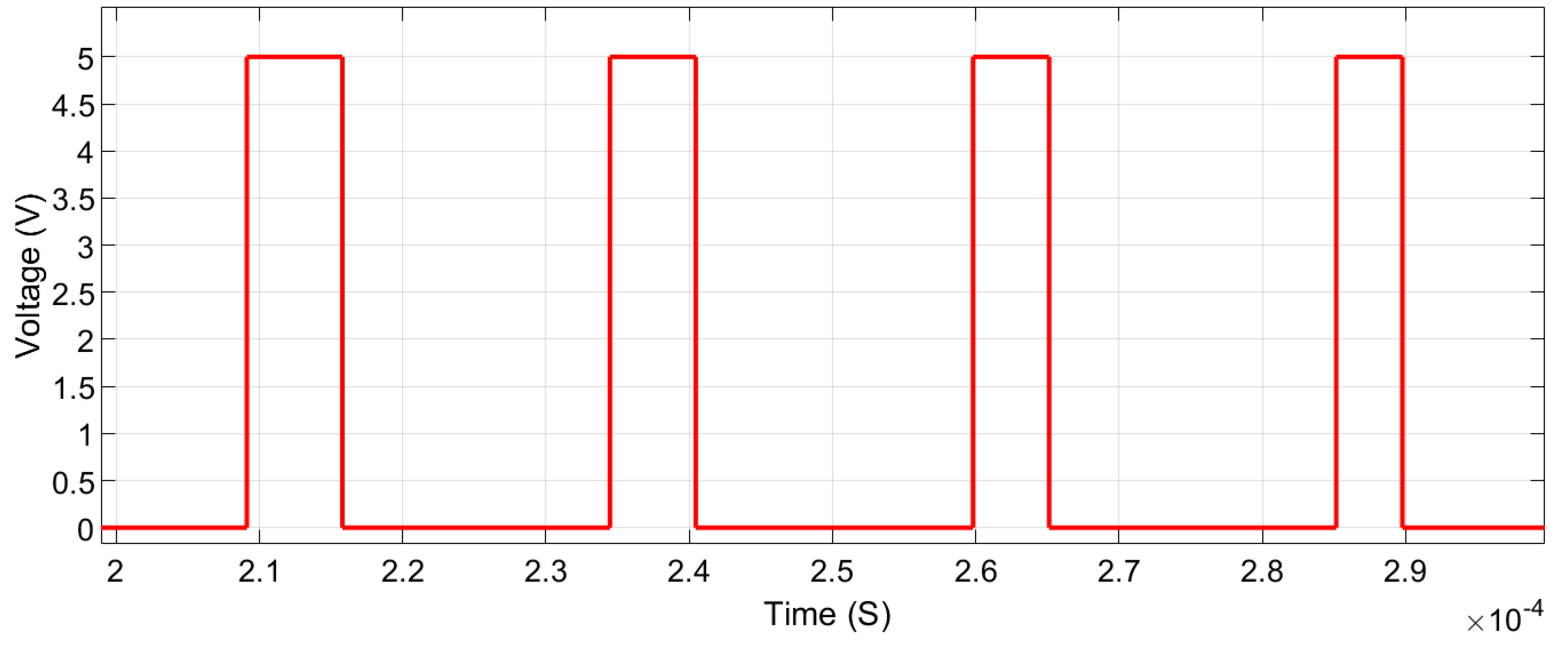
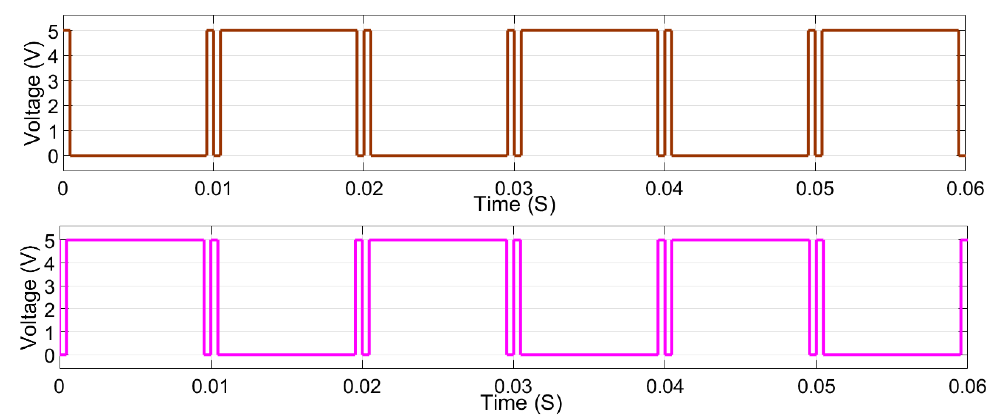
This section presents the simulation and experimental results of the proposed MLI. The simulation parameters used for the 15 levels are represented in Table 4. The simulation was conducted in MATLAB 2021a Simulink with a resistive load. Simulations were performed for the proposed inverter in MATLAB/Simulink to verify the inverter configuration. The simulations up to 15 levels used the algorithm outlined in Section 4, which could be expanded to every additional level needed. The setting up for both the simulation and the experiment was identical. Figure 11 and Figure 12 illustrate the generated high-frequency PWM pulses for the top inverter primary switches PS1 to PS4. The bottom inverter was run at a low frequency, whereas the top inverter operated at a high switching rate identical to the carrier frequency (10 kHz). Figure 13 and Figure 14 illustrate the generated low-frequency PWM pulses for the bottom inverter primary switches PS5 to PS8. Figure 15 illustrates the low-frequency PWM pulses generated for the bottom inverter secondary switches SS1 and SS2. The upper and lower inverter waveforms for a 15-level inverter and the final waveforms had a modulation index of 1. The output voltage levels fell as the quantity of “m” continued to decrease the resulting output voltage across the load, and the voltage output at the top inverter, the voltage output at the bottom inverter, and the load current waveform are displayed in Figure 16. The previously mentioned results were reached by assuming that each capacitor in the H-bridge inverter had its own independent DC source. Nevertheless, the generalized PWM switching approach and the improved modulation technique were employed to provide the proposed H-bridge inverter with one independent DC source.
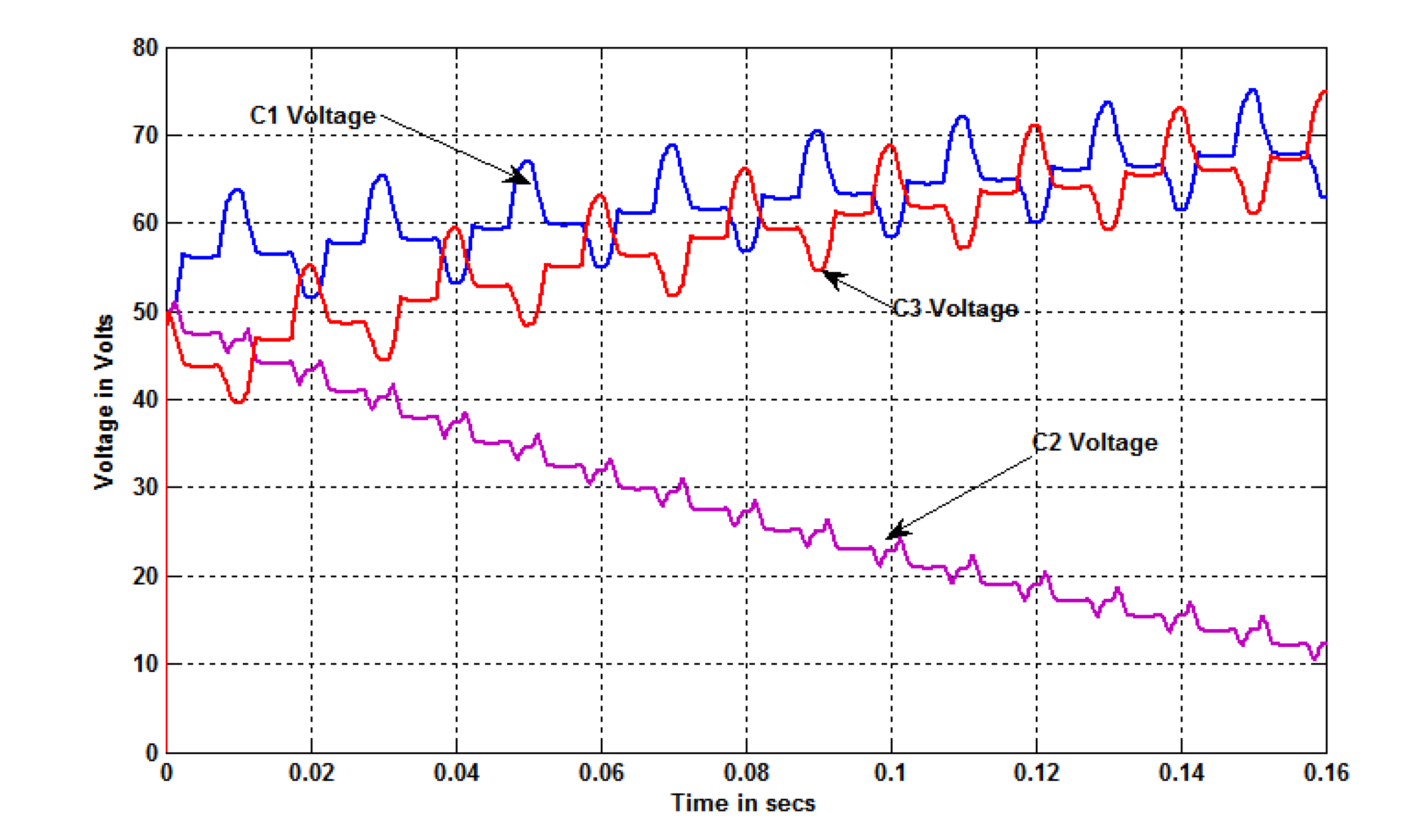
Figure 17 shows the output voltages at the capacitors without implementing the CVB approach. When using the generalized PWM method, it can be seen that although the C1 and C3’s capacitor voltages continually charged, C2 drained continuously. Figure 18 shows the output voltages at the capacitors with the implementation of the CVB algorithm. It depicts the voltages across the proposed MLI’s capacitors. At the same time, it was powered by an integrated conventional and improved switching approach, showing how closely spaced the capacitor voltages were to one another.

6. Hardware Validation

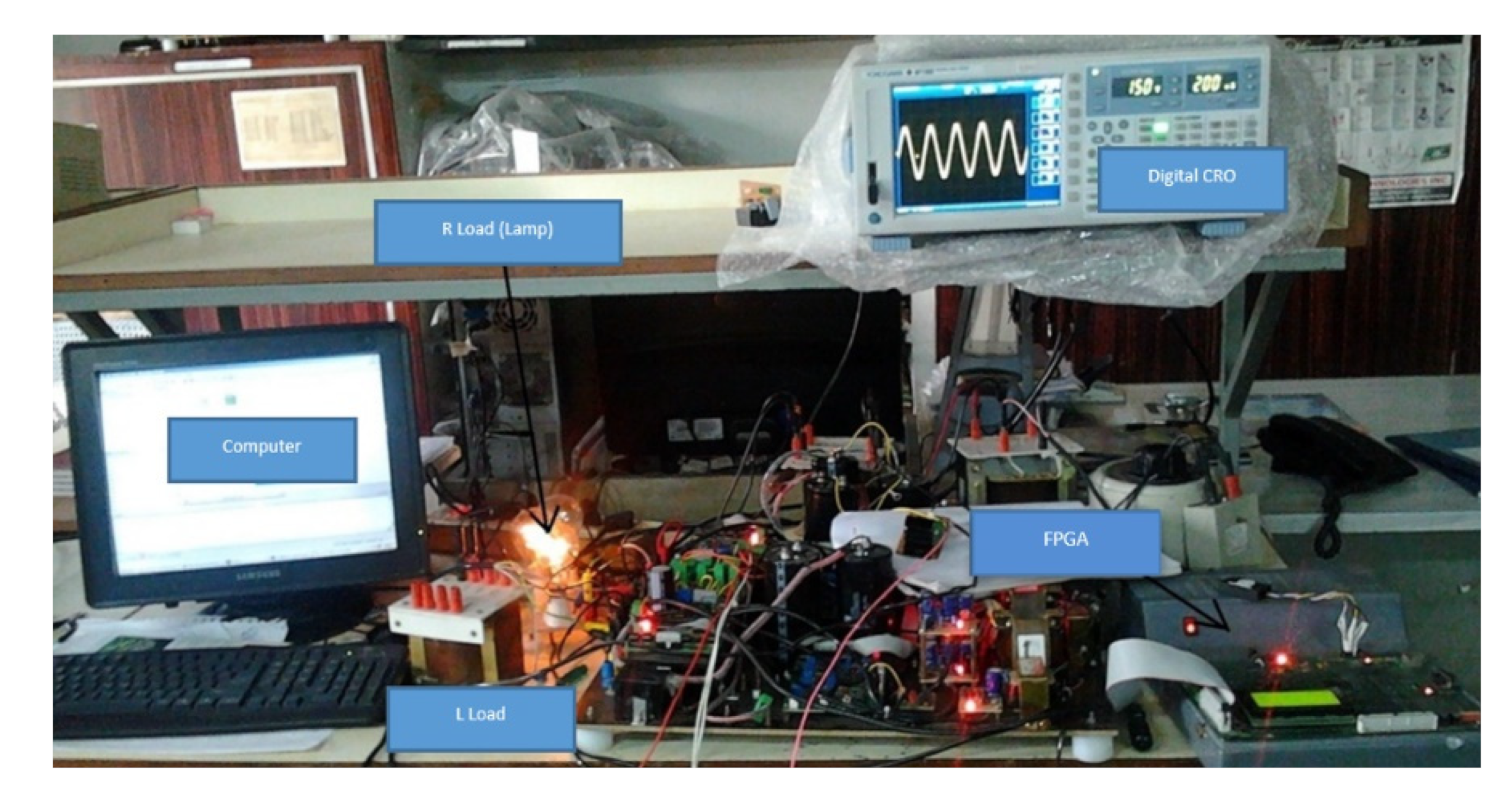
The proposed MLI was designed for a power of 2000 W with two asymmetrical DC input voltages of 47 V for the top inverter and 94 V × 3 for the bottom inverter, and the cascaded output voltage was obtained with equal discrete steps. Figure 19 depicts the block diagram of the hardware setup of the proposed converter. Figure 20 displays an image of the hardware configuration for the proposed d inverter with 15 levels constructed in the laboratory. The top and bottom inverters employed IGBTs from the MKI 80-06T6K series. A FIO50-12BD bidirectional secondary switch was employed in the bottom inverter. A SPARTAN 3A FPGA kit was used to create the gate-driving signal.
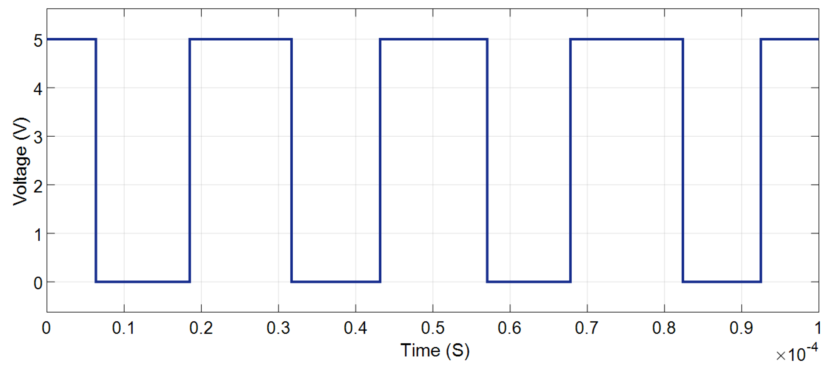
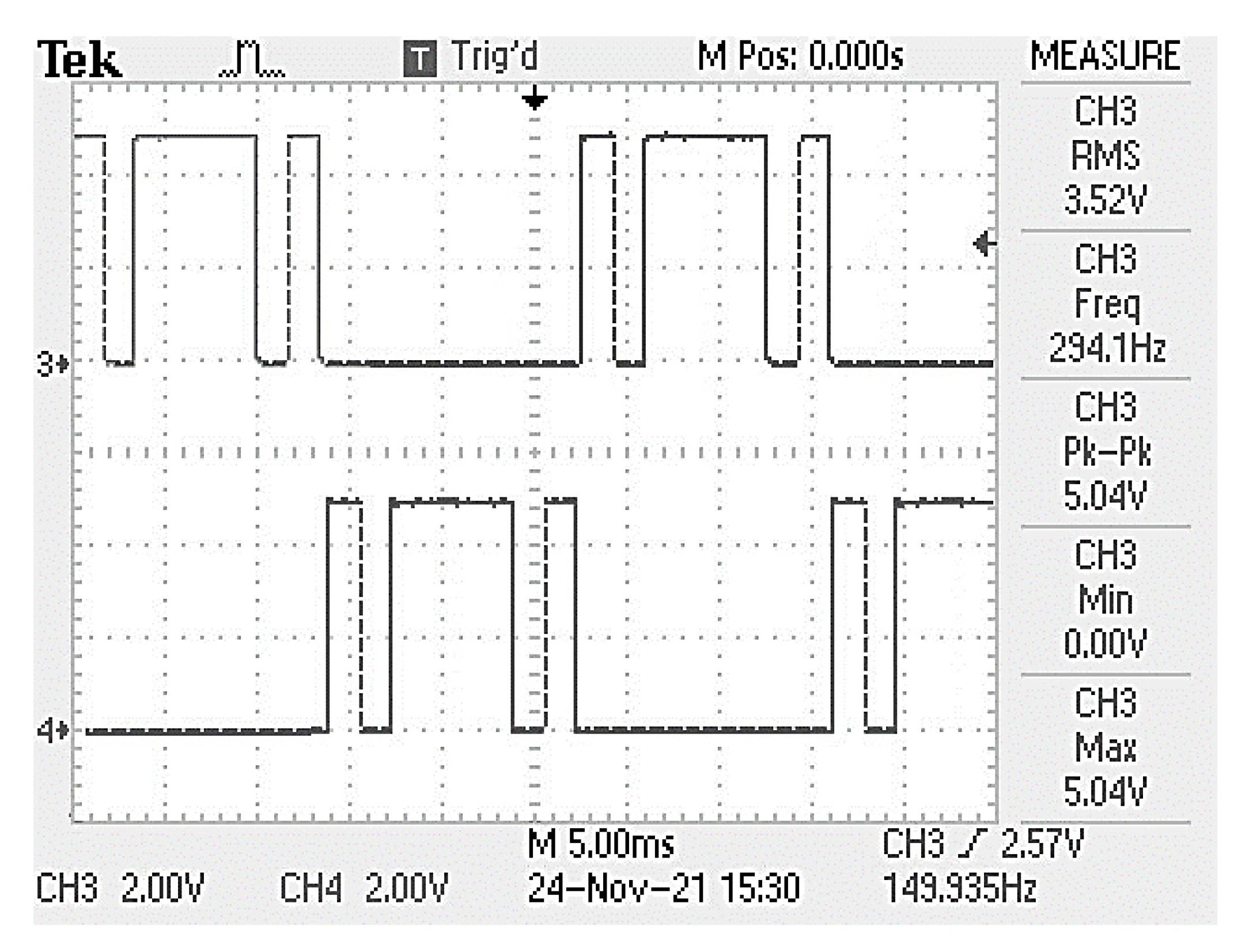
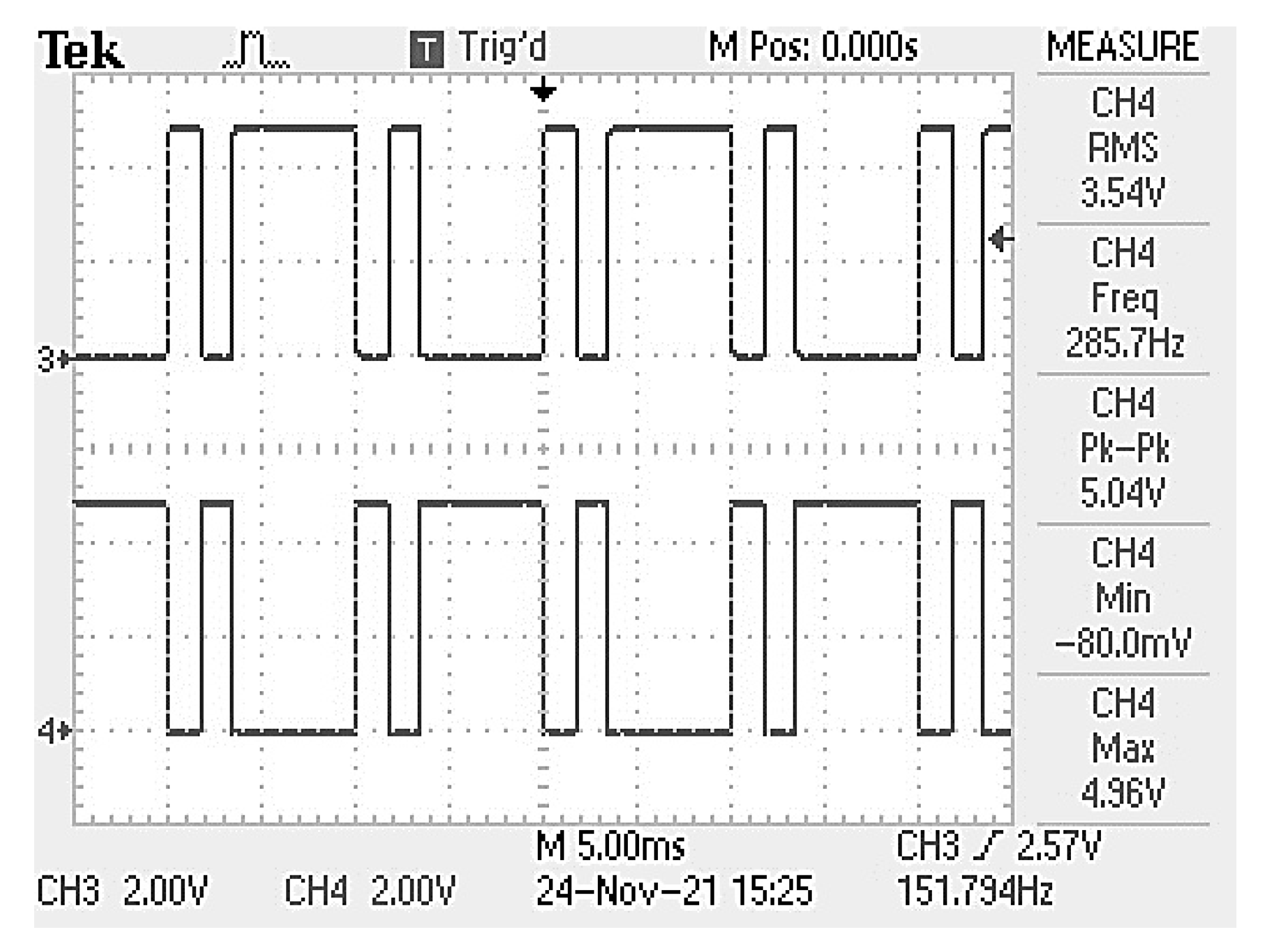
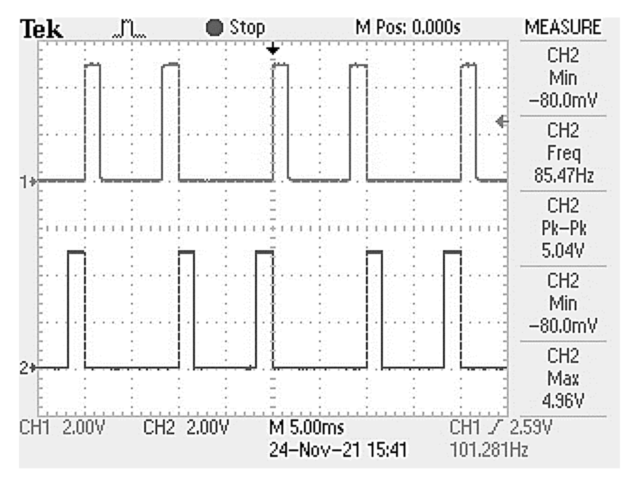
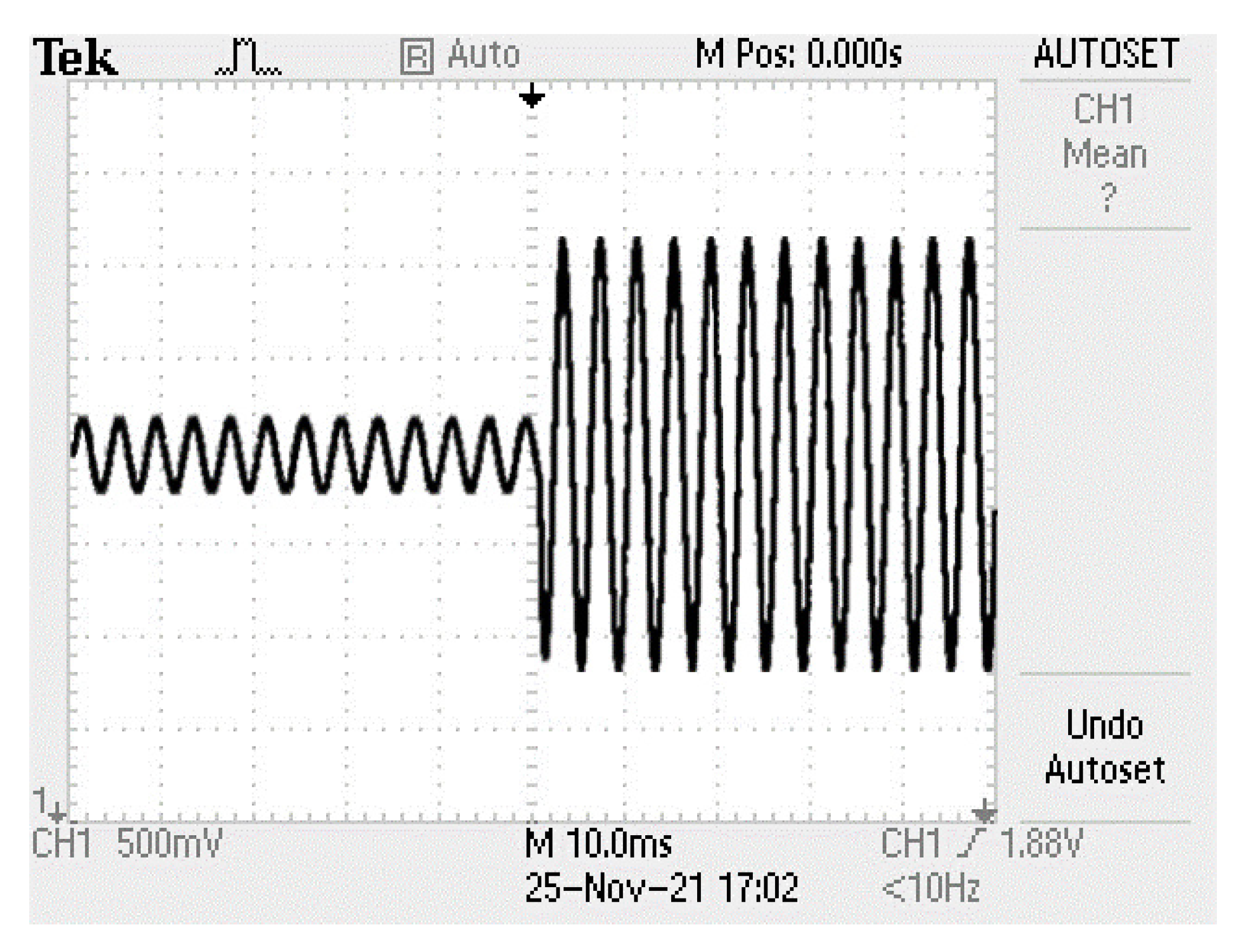
Figure 21 and Figure 22 depict the experimental findings of a 15-level inverter for upper inverters (PS1, PS3, PS2, and PS4). The switching pulses were produced for the high frequency of the top inverters while operating using the CVB technique. The switching frequency was maintained as 9.996 KHz for the upper switches (1 Div = 2 V). Figure 23 and Figure 24 depict the experimental results of the PWM waveform for the bottom inverters (PS5, PS7, PS6, and PS8). The switching voltages for the lower inverters were 5 V with (1 Div = 2 V). It showed that it maintained constant voltage while applying the lower switches with the help of CBV. The secondary switches’ PWM waveforms are illustrated in Figure 25. It operated at a low frequency of 101.381 Hz (1 Div = 2 V). It showed that while applying the CVB algorithm, the auxiliary switches operated at a high frequency, and the remaining switches operated at a low frequency. The output voltage of the proposed inverter, while controlled by the CVB methodology, is shown in Figure 26. In addition to the load current waveform, it also displayed the high- and low-frequency inverter waveforms. It was seen that the lower-frequency inverter output momentarily switched to a high frequency [29,30,31]. Figure 27 shows the hardware results of the capacitance voltages when the load was rapidly raised from 5 KW to 10 KW. It was clear that regardless of the case of an immediate load shift, the capacitor voltage only slightly deviated from its initial value before returning to it.
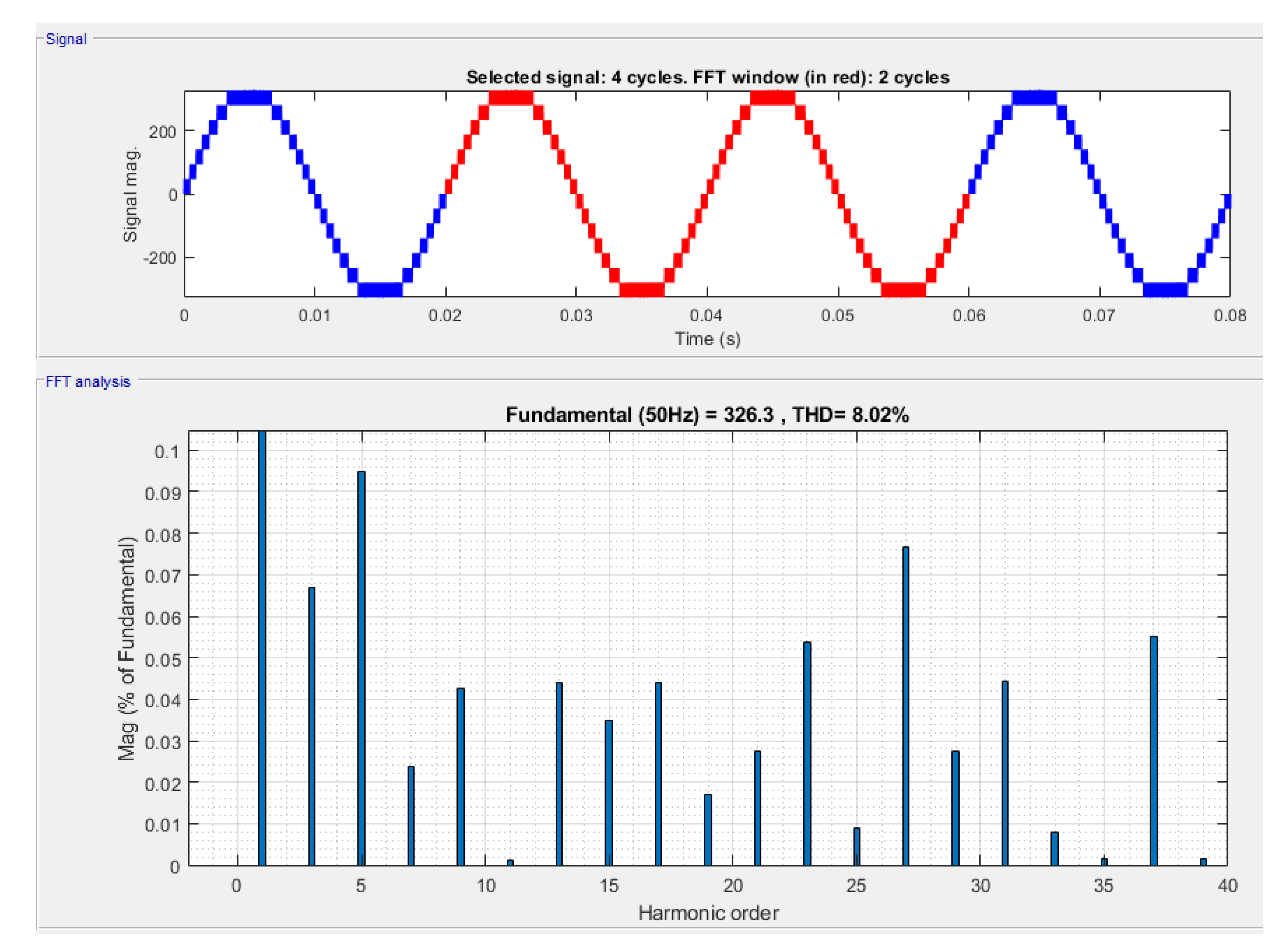
The FFT analyses of the output voltage for the 11- and 15-level inverters are shown in Figure 28 and Figure 29. The total harmonic distortions (THDs) of 11.36% and 8.02% were obtained for a fundamental frequency of 50 Hz. Without utilizing substantial voltage filters at the output, the load voltage was reached with a symmetrical voltage step equal to 100 V. The load current waveform with its harmonic spectra was reduced for a proposed MLI with a load of 5 kW and 0.8 LPF.
Table 5 details the current THD and the number of switches required for the 11- and 15-level inverters. The current THD values were 0.88 and 2.41 for 15 and 11 MLI, respectively. Table 6 demonstrates that the proposed topology outperformed the alternative topologies regarding switching devices and THD. In the MLI topologies, as the level increased, the THD reduced, and the decreased THD offered higher performance and power quality.

7. Conclusions

MLI provides improved output waveforms with a low THD. This study proposed a novel PWM technique for cascaded MLI with the few discrete DC sources and power electronics components possible. The capacitor voltages were also balanced using cutting-edge voltage balancing technology. The 15-level inverter converted a DC input voltage into a sinusoidal waveform with a lower THD of 8.02% compared with an 11-level MLI. The proposed inverter was simulated using MATLAB/Simulink, and experimental results were obtained, which were consistent with the simulation. The gate signals for the simulated inverter were generated using a SPARTAN 3A FPGA board, and these pulses were used to obtain the 15-level output of the inverter. The method balanced the capacitor voltages; hence, the generated inverter did not need extra multi-outlet DC–DC converters. The proposed inverter has various benefits apart from fewer components; it can be smaller and cost less and can have fewer switching losses and higher efficiency. As a result, applications requiring high and medium power can be employed with the proposed inverter. In future, this work can be extended to apply power balancing and machine learning approaches for controlling and diagnosing various faults in MLI.

Author Contributions

Conceptualization, S.K.R.; methodology, G.C.R.I.; investigation, G.C.R.I. and P.G.; writing—original draft preparation, S.K.R. and I.V; writing—review and editing, S.K.R.; resources, I.V.; visualization and administration, I.V. and M.L.A.; funding acquisition, M.L.A. All authors have read and agreed to the published version of the manuscript.

Funding

This research was funded by the Deputyship for Research & Innovation, Ministry of Education in Saudi Arabia for funding this research work through project number 223202.

Institutional Review Board Statement

Not applicable.

Informed Consent Statement

Not applicable.

Data Availability Statement

Not applicable.

Acknowledgments

The authors extend their appreciation to the Deputyship for Research & Innovation, Ministry of Education in Saudi Arabia for funding this research work through project number 223202.

Conflicts of Interest

There are no conflicts of interest declared by the authors.

References

  1. Almehizia, A.A.; Al-Masri, H.M.; Ehsani, M. Feasibility Study of sustainable energy sources in a fossil fuel rich country. IEEE Trans. Ind. Appl. 2019, 55, 4433–4440. [Google Scholar] [CrossRef] [Green Version]
  2. Kumar, B.R.; Sundararaju, K.; Saravanan, S.; Senthil Kumar, R. Mboa based PV array interconnection scheme for enlarging the harvested power under PS condition. Int. J. Electron. 2022, 110, 26–53. [Google Scholar]
  3. Podder, A.K.; Roy, N.K.; Pota, H.R. MPPT methods for solar PV systems: A critical review based on tracking nature. IET Renew. Power Gener. 2019, 13, 1615–1632. [Google Scholar] [CrossRef]
  4. Alzahrani, A.; Ramu, S.K.; Devarajan, G.; Vairavasundaram, I.; Vairavasundaram, S. A review on hydrogen-based hybrid microgrid system: Topologies for hydrogen energy storage, integration, and energy management with solar and wind energy. Energies 2022, 15, 7979. [Google Scholar] [CrossRef]
  5. Ramu, S.K.; Paramasivam, S.; Muthusamy, S.; Panchal, H.; Sadasivuni, K.K.; Noorollahi, Y. A novel design of switched boost action based multiport converter using dsPIC controller for Renewable Energy Applications. Energy Sources Part A Recovery Util. Environ. Eff. 2021, 44, 75–90. [Google Scholar] [CrossRef]
  6. Rong, F.; Gong, X.; Huang, S. A novel grid-connected PV system based on MMC to get the maximum power under partial shading conditions. IEEE Trans. Power Electron. 2017, 32, 4320–4333. [Google Scholar] [CrossRef]
  7. Farivar, G.; Hredzak, B.; Agelidis, V.G. A DC-side sensorless cascaded H-bridge multilevel converter-based Photovoltaic System. IEEE Trans. Ind. Electron. 2016, 63, 4233–4241. [Google Scholar] [CrossRef]
  8. Can, E. Mathematical algorithm of Fuzzy Logic Controller for multilevel inverter creating vertical divided voltage. Acta Polytech. 2019, 59, 1–11. [Google Scholar] [CrossRef] [Green Version]
  9. Can, E. Novel high multilevel inverters investigated on simulation. Electr. Eng. 2016, 99, 633–638. [Google Scholar] [CrossRef]
  10. Bendyk, M.S.; Luk, P.C.-K.; Alkhafaji, M.H. Control strategy for a modified Cascade multilevel inverter with dual DC source for enhanced Drivetrain Operation. IEEE Trans. Ind. Appl. 2017, 53, 4655–4664. [Google Scholar] [CrossRef] [Green Version]
  11. Can, E.; Sayan, H.H. A novel SSPWM controlling inverter running nonlinear device. Electr. Eng. 2016, 100, 39–46. [Google Scholar] [CrossRef]
  12. Yu, Y.; Konstantinou, G.; Hredzak, B.; Agelidis, V.G. Power balance of cascaded H-bridge multilevel converters for large-scale photovoltaic integration. IEEE Trans. Power Electron. 2016, 31, 292–303. [Google Scholar] [CrossRef] [Green Version]
  13. Yu, Y.; Konstantinou, G.; Hredzak, B.; Agelidis, V.G. Operation of cascaded H-bridge multilevel converters for large-scale photovoltaic power plants under bridge failures. IEEE Trans. Ind. Electron. 2015, 62, 7228–7236. [Google Scholar] [CrossRef]
  14. Kaliamoorthy, M.; Rajasekaran, V.; Raj, I.G.C. Single-phase fifteen-level grid-connected inverter for photovoltaic system with evolutionary programming based MPPT algorithm. Sol. Energy 2014, 105, 314–329. [Google Scholar] [CrossRef]
  15. Kaliamoorthy, M.; Rajasekaran, V.; Christopher Raj, I.G.; Hubert Tony Raj, L. Generalised hybrid switching topology for a single-phase Modular Multilevel Inverter. IET Power Electron. 2014, 7, 2472–2485. [Google Scholar] [CrossRef]
  16. Ramu, S.K.; Irudayaraj, G.C.; Paramasivam, S.K.; Murugesan, R.; Muthusamy, S.; Sundararajan, S.C.; Panchal, H.; Sadasivuni, K.K.; Meena, R.S. A simplified methodology for renewable energy integration and harmonic current reduction in Hybrid Micro Grid. Energy Sources Part A Recovery Util. Environ. Eff. 2021, 44, 8357–8379. [Google Scholar] [CrossRef]
  17. Hu, P.; Teodorescu, R.; Wang, S.; Li, S.; Guerrero, J.M. A currentless sorting and selection-based capacitor-voltage-balancing method for modular multilevel converters. IEEE Trans. Power Electron. 2019, 34, 1022–1025. [Google Scholar] [CrossRef] [Green Version]
  18. Peftitsis, D.; Tolstoy, G.; Antonopoulos, A.; Rabkowski, J.; Jang-Kwon, L.; Bakowski, M.; Ängquist, L.; Nee, H. High-power modular multilevel converters with SIC JFETs. IEEE Trans. Power Electron. 2012, 27, 28–36. [Google Scholar] [CrossRef] [Green Version]
  19. Can, E.; Sayan, H.H. Development of fractional sinus pulse width modulation with β gap on three step signal processing. Int. J. Electron. 2022, 110, 527–546. [Google Scholar] [CrossRef]
  20. Can, E. A new multi-level inverter with reverse connected dual DC to DC converter at simulation. Int. J. Model. Simul. 2020, 42, 34–46. [Google Scholar] [CrossRef]
  21. Can, E.; Sayan, H.H. Investigation of the effect of the gap at the zero-crossing point of pwms creating the first level voltage in a multi-level inverter. J. Eng. Res. 2022. [Google Scholar] [CrossRef]
  22. Anand, I.; Senthilkumar, S.; Biswas, D.; Kaliamoorthy, M. Dynamic Power Management System employing a single-stage power converter for standalone solar PV applications. IEEE Trans. Power Electron. 2018, 33, 10352–10362. [Google Scholar] [CrossRef]
  23. Hinago, Y.; Koizumi, H. A single-phase multilevel inverter using switched series/parallel DC voltage sources. IEEE Trans. Ind. Electron. 2010, 57, 2643–2650. [Google Scholar] [CrossRef]
  24. Sabyasachi, S.; Borghate, V.B.; Karasani, R.R.; Maddugari, S.K.; Suryawanshi, H.M. Hybrid control technique-based three-phase cascaded multilevel inverter topology. IEEE Access 2017, 5, 26912–26921. [Google Scholar] [CrossRef]
  25. Agrawal, N.; Bansal, P. A new 21-level asymmetrical multilevel inverter topology with different PWM techniques. In Proceedings of the 2017 Recent Developments in Control, Automation & Power Engineering (RDCAPE), Noida, India, 26–27 October 2017. [Google Scholar]
  26. Reddy, V.P.; Muralikumar, K.; Ponnambalam, P.; Mahapatra, A. Asymmetric 15-level multilevel inverter with fuzzy controller using super imposed carrier PWM. In Proceedings of the 2017 Innovations in Power and Advanced Computing Technologies (i-PACT), Vellore, India, 21–22 April 2017. [Google Scholar]
  27. Saravanan, S.; Senthil Kumar, R.; Prakash, A.; Chinnadurai, T.; Tiwari, R.; Prabaharan, N.; Chitti Babu, B. Photovoltaic array reconfiguration to extract maximum power under partially shaded conditions. In Distributed Energy Resources in Microgrids; Academic Press: Cambridge, MA, USA, 2019; pp. 215–241. [Google Scholar]
  28. Sarasvathy, K.; Luciana, M.L.; Kumar, R.S. Comparison of sine, hysteresis, SVPWM and predictive PWM techniques for shunt active power filter. In Proceedings of the 2017 IEEE International Conference on Electrical, Instrumentation and Communication Engineering (ICEICE), Karur, India, 27–28 April 2017. [Google Scholar]
  29. Alghaythi, M.L.; O’Connell, R.M.; Islam, N.E.; Khan, M.M.S.; Guerrero, J.M. A High Step-Up Interleaved DC–DC Converter with Voltage Multiplier and Coupled Inductors for Renewable Energy Systems. IEEE Access 2020, 8, 123165–123174. [Google Scholar] [CrossRef]
  30. Alghaythi, M.L.; O’Connell, R.M.; Islam, N.E. Design of a High Step-up DC-DC Power Converter with Voltage Multiplier Cells and Reduced Losses on Semiconductors for Photovoltaic Systems. In Proceedings of the 2019 IEEE Electric Ship Technologies Symposium (ESTS), Arlington, VA, USA, 14–16 August 2019; pp. 214–218. [Google Scholar]
  31. Najwan Hamidi, M.; Ishak, D.; Ammirrul Atiqi Mohd Zainuri, M.; Ai Ooi, C.; Tarmizi, T. Asymmetrical multi-level DC-link inverter for PV Energy System with perturb and observe based voltage regulator and capacitor compensator. J. Mod. Power Syst. Clean Energy 2021, 9, 199–209. [Google Scholar] [CrossRef]
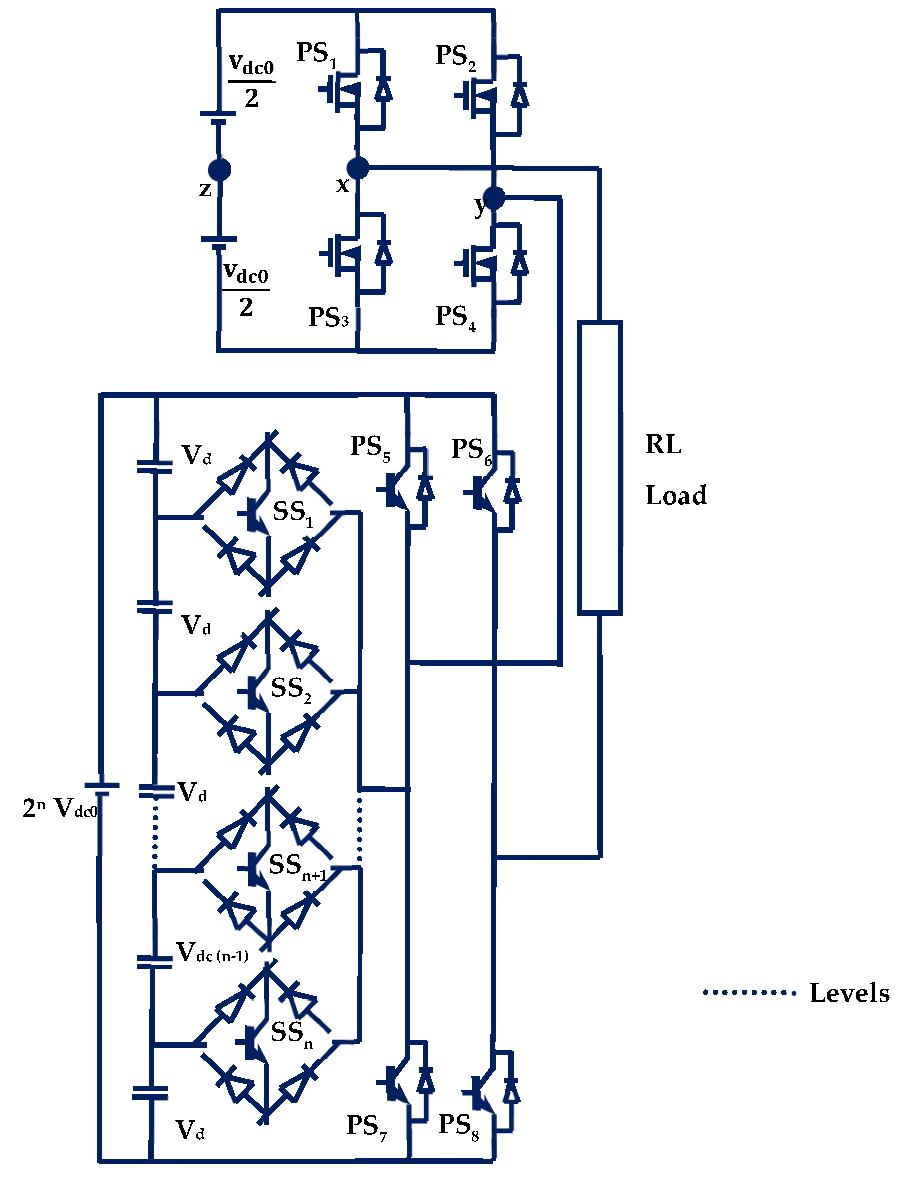
Figure 1. Proposed cascaded H-bridge multilevel inverter.
Sustainability 15 10698 g001
Figure 2. Mode of operation.
Sustainability 15 10698 g002
Figure 3. Predicted seven-stage output voltage waveform.
Sustainability 15 10698 g003
Figure 4. Direction of current flow path during mode 2 (🟥🟥🟥🟥🟥 Charging, 🟦🟦🟦🟦🟦 Discharging).
Sustainability 15 10698 g004
Figure 5. Direction of current flow path during mode 3 (🟥🟥🟥🟥🟥 Charging, 🟦🟦🟦🟦🟦 Discharging).
Sustainability 15 10698 g005
Figure 6. Direction of current flow path during mode 5 (🟥🟥🟥🟥🟥 Charging, 🟦🟦🟦🟦🟦 Discharging).
Sustainability 15 10698 g006
Figure 7. Direction of current flow path during mode 6 (🟥🟥🟥🟥🟥 Charging, 🟦🟦🟦🟦🟦 Discharging).
Sustainability 15 10698 g007
Figure 8. Proposed modified switching technique cascading top and bottom inverter.
Sustainability 15 10698 g008
Figure 9. Top and bottom voltage waveforms and cascaded output by using modified switching technique.
Sustainability 15 10698 g009
Figure 10. Generated PWM switching signals for switches.
Sustainability 15 10698 g010
Figure 11. High-frequency top inverter PWM for PS1 and PS3.
Sustainability 15 10698 g011
Figure 12. High-frequency top inverter PWM for PS2 and PS4.
Sustainability 15 10698 g012
Figure 13. Low-frequency bottom inverter PWM for PS5 and PS7.
Sustainability 15 10698 g013
Figure 14. Low-frequency bottom inverter PWM for PS6 and PS8.
Sustainability 15 10698 g014
Figure 15. Bottom inverter PWM for SS1 and SS2.
Sustainability 15 10698 g015
Figure 16. The 15-level inverter: (a) Obtained output voltage across the load. (b) Obtained voltage at the top inverter. (c) Obtained voltage at the bottom inverter. (d) Obtained load current waveform.
Sustainability 15 10698 g016
Figure 17. Capacitor voltage at the bottom inverter without balancing.
Sustainability 15 10698 g017
Figure 18. Capacitor voltage at the bottom inverter with balancing.
Sustainability 15 10698 g018
Figure 19. Hardware block setup of the proposed inverter.
Sustainability 15 10698 g019
Figure 20. Hardware prototype model of the proposed inverter.
Sustainability 15 10698 g020
Figure 21. High-frequency top inverter PWM for PS1 and PS3.
Sustainability 15 10698 g021
Figure 22. High-frequency top inverter PWM for PS2 and PS4.
Sustainability 15 10698 g022
Figure 23. Low-frequency bottom inverter PWM for PS5 and PS7.
Sustainability 15 10698 g023
Figure 24. Low-frequency bottom inverter PWM for PS6 and PS8.
Sustainability 15 10698 g024
Figure 25. Bottom inverter PWM for SS1 and SS2.
Sustainability 15 10698 g025
Figure 26. (a) Output voltage at the bottom inverter. (b) Voltage at the top inverter. (c) Output voltage across the load. (d) Load current hardware waveform.
Sustainability 15 10698 g026
Figure 27. Output current with load variation.
Sustainability 15 10698 g027
Figure 28. FFT analysis for 11-level inverter.
Sustainability 15 10698 g028
Figure 29. FFT analysis for 15-level inverter.
Sustainability 15 10698 g029
Table 1. Switching modes of bottom H-bridge inverter.
Switching ModePS5PS6PS7PS8SS1SS2Voltage ObtainedReference
10Figure 2a
0Figure 2b
22 Vdc0Figure 2c
34 Vdc0Figure 2d
46 Vdc0Figure 2e
5−2 Vdc0Figure 2f
6−4 Vdc0Figure 2g
7−6 Vdc0Figure 2h
✖—OFF|✓—ON
Table 2. Capacitor charging and discharging status of capacitors.
Switching ModePS5PS6PS7PS8SS1SS2Status of CapacitorsTime Duration
C1C2C3
1UCUCUC1.84 ms
UCUCUC
21.92 ms
32.26 ms
4UCUCUC4.9 ms
51.92 ms
62.26 ms
7UCUCUC4.9 ms
❌—OFF|✓—ON|UC—Unchanged20 ms
Table 3. Switching states and expected output of 15-level inverter.
Top H Bridge SwitchesBottom H Bridge SwitchesModeOutput Load Voltage V d c 1 = V d c 2 = V d c 3 = 2 V d c 0   i . e . ,   V d c n V d c 0 = 2
PS1PS2PS3PS4PS5PS6PS7PS8SS1SS2VtopVbottomVtotal = Vtop + Vbottom
I 0 V dc 0 6 Vdc0 6 V dc 0   7 V dc 0
II V dc 0 0 6 Vdc0 5 V dc 0   6 V dc 0
III 0 V dc 0 4 V dc 0 6 V dc 0 4 V dc 0   5 V dc 0
IV V dc 0 0 2 V dc 0 4 V dc 0   3 V dc 0 4 V dc 0  
V 0 V dc 0 2 Vdc0 2 V dc 0 3 V dc 0  
VI V dc 0 0 2 Vdc0 V dc 0 2 V dc 0  
VII 0 V dc 0 0 0 V dc 0
VIII 0 V dc 0 0 0 V dc 0
IX V dc 0 0 −2 Vdc0 V dc 0 2 V dc 0  
X 0 V dc 0 −2 Vdc0 2 V dc 0 3 V dc 0  
XI V dc 0 0 2 V dc 0 4 V dc 0 3 V dc 0 4 V dc 0  
XII 0 V dc 0 4 V dc 0 6 V dc 0 4 V dc 0 5 V dc 0  
XIII V dc 0 0 −6 Vdc0 5 V dc 0 6 V dc 0  
XIV 0 V dc 0 −6 Vdc0 6 V dc 0 7 V dc 0  
✖—OFF|✓—ON
Table 4. Simulation parameters.
PARAMETERSLEVEL 11LEVEL 15
Top inverter voltage65 V47 V
Bottom inverter voltage130 V94 V
Load resistance = 100 Ω and load inductance = 30 mH.
Table 5. Voltage THD for 11- and 15-level inverters.
LevelsNo. of Primary Switches in the Top InverterNo. of Primary Switches in the Bottom InverterNo. of Secondary Switches in the BottomCurrent THD in %
154420.88
114412.41
Table 6. THD comparison of various 15-level MLIs with the proposed inverter.
Previous WorkLevelsTotal No. of
Switches Used
Total DC
Sources
Current THD in %
[9]151032.32
[10]151031.83
[17]151031.08
Proposed151020.88
Disclaimer/Publisher’s Note: The statements, opinions and data contained in all publications are solely those of the individual author(s) and contributor(s) and not of MDPI and/or the editor(s). MDPI and/or the editor(s) disclaim responsibility for any injury to people or property resulting from any ideas, methods, instructions or products referred to in the content.