Abstract
Small-signal models of dc-dc converters are often designed using a state-space averaging approach. This design can help discuss and derive the control-oriented and other frequency-domain attributes, such as input or output impedance parameters. This paper aims to model the dc-dc converters for PV application by employing a capacitor on the input side. The modeling, design, and analysis of the dc-dc converters regarding the input capacitor is limited in the literature. Five dc-dc converters, including buck, boost, buck-boost, ĆUK, and SEPIC converters, are designed and implemented using the state-space average modeling approach in MATLAB/Simulink. The circuit topology of each converter and the state-space matrices are derived considering every constraint. A rigorous and compelling analysis of the dc-dc converters is carried out to compare system stability and, ultimately, the dynamic performance. The output of the resulting small-signal models has been demonstrated in the time-domain against topology simulations. All the converters are exposed to unpredictable weather conditions and the simulations are carried out in the PSIM software. The perturb and observe (P&O) maximum power point tracking (MPPT) algorithm is applied in all the converters to ensure maximum power point (MPP) achievement. The results showcase that the boost converter outperforms all other converters in terms of stability, settling time, and overshoot.
1. Introduction
Photovoltaic (PV) energy is an excellent resource for cost-effective and clean electricity production because it is inherently noise-free, environmentally friendly, flexible scaling, sustainability, and low-maintenance. The PV system displays non-linear current vs. voltage (I–V) characteristics due to its dependency on irradiation level, temperature, and load conditions []. Researchers have proposed techniques and models to improve the designs and integration of PV modules and converters in a broader spectrum [,,]. Research work differs in terms of sensor requirement, convergence time, hardware complexity, and other domains [,,].
The switching performance of the dc-dc converters usually varies around 70% to 95% due to their non-ideal behavior []. The current value cannot suddenly drop to zero due to switching times and conduction mode resistance, and thus incurs power loss. However, their performance can be boosted by observing their behavior. Designing power converters is complicated because of the requirement to analyze various time-variant circuital configurations based on the switching performance of semiconductor switches transistors and diodes [,,]. Therefore, the modeling of power electronic circuits comes under non-linear structure systems as sudden changes are introduced in their differential equations [,,,]. The mathematical modeling of DC-DC converters is a crucial step in the design and analysis of these electronic devices. In fact, there are several reasons why mathematical modeling is performed for DC-DC converters, such as:
- To understand the behavior and dynamics of DC-DC converters under different operating conditions.
- To simulate the behavior of the DC-DC converter before building a physical prototype.
- To facilitate the analysis of the converter’s performance metrics, such as its efficiency, voltage regulation, and transient response.
- To facilitate the design and analysis of control algorithms to achieve stable and desired system behavior.
- To perform sensitivity analysis to understand how variations in component values and parameters affect the performance of the converter. This information is valuable for robust design.
- Mathematical models help us to analyze the transient response of the system, ensuring that it meets the required specifications.
- Mathematical models are used in educational settings to teach students about the principles of DC-DC converters. They also serve as a foundation for research in power electronics and related fields.
The mathematical equations also form the basis for model predictive control (MPC) systems [,]. The standard methods are unable to provide an authentic solution due to these time and state discontinuities.
The two great modeling techniques for small-signal dc-dc converters include state-space averaging and switch averaging [,,]. The switch-mode converters possess non-linear properties, mainly due to the passive elements and switching devices. Such converters can be modeled in either of the two modes: analytical or numerical. The numerical methods are dependent on simulations or several algorithms to generate results in terms of quantities [,,]. Though easy to implement, they do not provide the proper insight required to realize switching characteristics. Analytical techniques provide a platform where the converter’s performance and behavior can be well judged based on continuous-time techniques, mainly state-space averaging, circuit averaging, and pulse width modulation (PWM) switch modeling [].
The inherent nature of the dc-dc converters renders the switched modeling technique a poor choice for carrying out the steady-state input–output converter relationships directly or for extracting authentic information for the modeling of linear regulators []. State-space averaging is now significantly utilized to model dc-dc converters and has proven to be the most realistic approach for building small-signal models [,,]. Various extensions have been introduced in this method, such as designing converters that work under variable conditions []. The primary advantage added through these extensions suggests the averaging approach as the best choice, as the system analysis can be authenticated through a non-linear time-invariant continuous-time system, rather than depending on a discontinuous right-hand-side system such as the switched model. An advantage of using the state-space averaging method is the generality of its outcome. Once the converter state equations are appropriately written, it is guaranteed that a small-signal averaged model will be obtained.
The objective of this paper is to study, model, analyze, design, and simulate the behavior of five different non-isolated converters with appropriate input capacitor () design for a PV system. Note that when these converters are interfaced with a mostly constant current source like a PV module, an additional capacitor () is required at the input. The inclusion of an energy storage element in the system alters the dynamics of the dc-dc converter. This makes it complex compared to the voltage-fed dc-dc converters. Consequently, if same techniques are applied on the current-fed converters, the holistic understanding of converter dynamics becomes unachievable. The state-space modeling is used to derive the characteristics function of converters. The significance of this study is to evaluate the performance and stability of converters when installed in the PV system. Such a comprehensive performance study for five converters with capacitor is limited in the literature. Consequently, this research work will deliver the insight about the correct selection of converter for different types of PV applications.
2. Modeling of DC-DC Converters
2.1. DC-DC Buck Converter
The converter’s name suggests that the output voltage results in a lower value than the input voltage. For this very reason, this converter is also known as a step-down voltage regulator. A buck converter has the benefit of coming up with non-isolated, switch-mode dc-dc conversion, resulting in a cost-effective and straightforward conversion [].
The operation involves switching that leads to two circuit formations alternately, allowing a path for the inductor to be connected to the source voltage to make the inductor capable of storing energy and later discharging the inductor into the load. Figure 1 presents a typical buck converter which consists of a switch (S), an inductor (L), a diode (D), an input capacitor (), an output capacitor (C), and a load resistance (). The state of the switch is controlled through a PWM control signal. The value of current through the L during the Continuous Conduction Mode (CCM) does not drop to zero within switching cycles. This situation results in an on-time state (on-mode) and off-time state (off-mode), presented in Figure 2.

Figure 1.
Typical buck converter.

Figure 2.
Modes of the buck converter (a) On-mode of the buck converter (b) Off-mode of the buck converter.
State equations for the on-mode of the buck converter are defined as
where is the current through L, is the voltage across , is the voltage across the PV panel, is the output voltage, and is the internal resistance. Using Equations (1)–(3), the ON-state equation of the buck converter is derived as
State-space equations for the OFF-state of the buck converter are written as
Using Equations (6)–(8), the OFF-state matrix of the buck converter is calculated as
There is a need to generate an average description of the circuit for a switching time-span. The equations representing the two ongoing states are subjected to two procedures that are time-weighted and averaged. The general equations used for this purpose are
where ‘d’ represents the duty cycle of the converter. Equations (11)–(14) are applied to derive averaged matrices for both modes of the buck converter from Equations (4), (5), (9) and (10).
Small ac perturbations are commenced in the dc steady-state components
As a linear method is assumed, the aim is to find the transfer function between the output voltage and the duty ratio; the perturbation is not introduced in the input voltage and is thus zero for the simplification []. To attain a steady-state equation, it is required to change the perturbation terms and their derivatives to zero.
2.2. DC-DC Boost Converter
The boost regulator finds its applications in the scenarios that require a higher output voltage compared to the input. Due to the non-linear and time-variant property of the boost converter, it is practical to design a linear controller to find a small signal model [,]. That model sets the direction for linearizing the state-space average model around an appropriate operating point.
This section deals with carrying out the state-space equations of a boost converter in both operating modes, on-mode and off-mode. It is pertinent to take all the system parameters into account, including the resistance of the inductor, capacitor, load, diode characteristics, switch-on resistance, voltage ratings, and load current. The coefficients of state-space equations will rely on the DC operating point and the circuit parameters []. It is not complicated to obtain the value of the duty ratio using these coefficients and later introduce it as an input.
Figure 3 represents a conventional boost converter, which consists of a switch (S), an inductor (L), a diode (D), an input capacitor (), an output capacitor (C), and a load (). Figure 4 presents the equivalent circuits of the boost converter during on-mode and off-mode. The switch position of the converter is controlled by a PWM of the time period (T) and duty cycle (d).
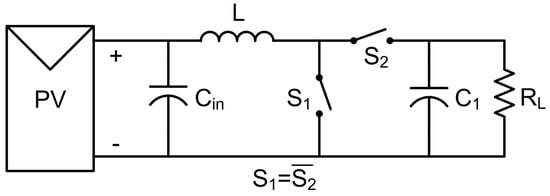
Figure 3.
Typical boost converter.

Figure 4.
Modes of the boost converter (a) On-mode of the boost converter (b) Off-mode of the boost converter.
It is mandatory to include state-space equations of both the modes that are on and off. These stages can further be represented as a single state-space description with the illustration of the circuit’s behavior over the time period, T. Using the circuit topology described in Figure 4, the on-state matrix is calculated as
where is the current through L, is the voltage across , is the voltage across the PV module, is the output voltage, and is the internal resistance. Using the circuit topology substantiated in Figure 4, the off-state matrix is derived as
The steady-state averaging method is utilized to obtain a converter model with a span of one switching period. Equations (11)–(14) are applied to compute averaged matrices from Equations (21)–(24),
By introducing small ac perturbations Equations (25) and (26) are modified to
2.3. Modeling of Buck-Boost Converter
Out of all the available dc-dc converters, the buck-boost regulator is preferred for applications where the output voltage is required to be higher or lower than the input voltage. Designing a controller for the buck-boost dc-dc converter is strenuous compared to designing one for the other converters, including buck or boost converters, since this converter carries a non-minimum phase system [].
A typical buck-boost converter is shown in Figure 5, which consists of a switch (S), an inductor (L), a diode (D), an input capacitor (), an output capacitor (), and a load (). Both working modes of the buck-boost converter are shown in Figure 6. It also shows the voltage polarities and current direction in both stages.
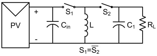
Figure 5.
Typical buck-boost converter.

Figure 6.
Modes of the buck-boost converter (a) On-mode of the buck-boost converter (b) Off-mode of the buck-boost converter.
The on-stage matrices for the buck-boost converter are computed as,
where is the current through L, is the voltage across , is the voltage across the PV module, is the output voltage, and is the internal resistance. The off-stage matrix is evaluated as
The modeling of a converter is based on the working state of the switches used, as it alters the configuration and working state of the whole circuit. This problem is managed using the circuit averaging technique known as the state-space averaging technique, as the dependent parameters are time-weighted. Equations (11)–(14) are applied to derive averaged matrices from Equations (29)–(32),
By introducing small ac perturbations, Equation (33) and (34) are modified to
2.4. Modeling of ĆUK Converter
A dc-dc ĆUK Converter has the ability to provide a regulated output voltage at a relatively lower or higher level than the input voltage level, with polarity of reversed [,]. Figure 7 represents the basic circuit of the ĆUK converter, which consists of a switch (S), two inductors ( and ), a diode (D), an input capacitor (), an energy-transferring capacitor (), an output capacitor (), and a load ().

Figure 7.
Typical ĆUK converter.
A ĆUK converter works in two switching stages. The on and off states are further determined considering the duty ratio and switching period. Figure 8 shows the equivalent circuit of the ĆUK converter during both stages.

Figure 8.
Operational Modes of the ĆUK converter (a) On-mode (b) Off-mode.
On-stage matrix for the ĆUK converter is written as
where is the current through , is the current through , is the voltage across , is the voltage across , is the voltage across the PV module, is the output voltage, and is the internal resistance. State matrices for the off-mode are evaluated as
The averaging method takes into account different sets of equations for all switched circuit configurations. A single equation is formed after analyzing and carrying out the linearly weighted average of the previous equations. Two equations are obtained considering the CCM of a ĆUK converter depending on both working states using the circuits in Figure 8. Equations (11)–(14) are applied to compute averaged matrices from Equations (37)–(40),
By introducing small ac perturbations, Equation (41) is modified to
2.5. Modeling of Sepic Converter
Single ended primary inductance converter (SEPIC) is a dc-dc voltage converter that is utilized for applications involving the criteria to buck, boost or permit the electrical voltage at the output side to reach the desired stage with a similar polarity as that of the input side [,]. The phrase “single-ended” indicates that only one switch directs energy trade between inductors and capacitors []. Figure 9 shows the circuit of a SEPIC converter, which consists of a switch (S), two inductors ( and ), a diode (D), an input capacitor (), an energy-transferring capacitor (), an output capacitor (), and a load ().

Figure 9.
Typical SEPIC converter.
In the case of a SEPIC converter, the wire resistance of the inductor is lower, and it consequently generates less energy in the form of heat that further results in higher efficiency [,]. In other words, a more significant part of the input power is transferred to the load side []. As there are two stages of operation, as mentioned in Figure 10, it is mandatory to consider both while considering state variables. The state variable description can be written by analyzing basic circuitry. It is to be noted that the internal resistances of the voltage source and other electronic components affect the output voltage generated. On-state matrix is given as
where is the current through , is the current through , is the voltage across , and is the voltage across . Using the circuit topology of the SEPIC converter, off-stage matrices are evaluated as
The average state matrix is computed using Equations (11)–(14)
By introducing small ac perturbations, Equation (48) is changed to

Figure 10.
Operational modes of a SEPIC converter. (a) On-mode (b) off-mode.
3. Designing of Converters
Design relations for all the components presented in the above-discussed converters are derived and presented in Table 1. The behavior of the converter is expressed through voltage gain relation, which is a function of , , and duty ratio D. The voltage gain relation of any converter can be transformed in terms of the impedance relation between internal resistance () of the PV module/array and load resistance (), as presented in Table 1. The inductor value () of each converter is derived through the volt-second product of the converter during either on-time state (on-mode) or off-time state (off-mode). For capacitors, the charge-second product of the converter is considered for designing during either on-time state (on-mode) or off-time state (off-mode) [,,]. These designed relations are well reported in the literature, with the exception of input capacitor (), which is installed at the input node in parallel with PV module/array. Now, if the input supply is continuous, as in the case of a boost converter, the size of is small, as presented in Table 1. On the other hand, if the input supply is discontinuous, as in the case of a buck converter, the size of the capacitor is large. This of other converters are designed according to the same approach.

Table 1.
Design relations of the discussed converters.
4. Simulation Results and Discussion
Kyocera KC200GT is adopted as an input model for the simulation with the specifications expressed in Table 2 []. This PV module is able to generate 200 W maximum power ( corresponding to a voltage () and current of 26.3 V and 7.61 A, respectively. The specifications also include the values of open circuit voltage () and short circuit current , which are mainly used to determine the worst-case scenarios in a PV plant. All these values are calculated at fixed values of irradiance and temperature, which are termed as standard testing conditions (STC) []. The STC conditions set irradiance at 1000 , cell temperature at 25 C and air mass 1.5. Several PV modules are connected in series and in parallel to create a PV array. The array size of Ns × Np = 2 × 3 is considered to carry out simulations, where Ns represents the number of modules in series, and Np is the number of modules in parallel. These array values are used to evaluate the design parameters of Table 1, and the results are substantiated in Table 3, where D = 0.7 and = 20 kHz.
One of the significant issues faced by electronic circuits is transient overshoot. It poses a threat of abrupt drift that results in performance degradation and sometimes unbearable loss in the circuit [,,]. The number of fluctuations in the output response increases with the order of the circuit. To address this issue, the pole-zero cancellation technique is utilized; this technique cancels out poles and zeros from the transfer function, thus reducing the order of the system. It is to be noted that with a more substantial imaginary component of the pole and a shorter duty cycle, the oscillations increase. Similarly, when dealing with a constant real-component of the pole, the overshoot and the settling time is comparatively less. The duty cycle increases with the decreasing imaginary part of the pole. It reduces the number of oscillations while the overshoot and settling time increases.
Figure 11 represents the step response of buck, boost, and buck-boost converters at the Maximum Power Point (MPP) calculated via MATLAB. The settling time () of the boost converter is the shortest compared to the buck and buck-boost converters. Out of the three converters, the buck converter presents maximum overshoot (OS), which is 69% compared to 23.5% OS of the boost converter and 47.1% of the buck-boost converter. Moreover, the rise time of the buck-boost converter is longer than that of the other two converters. Whether a system is deemed as stable, unstable, or relatively stable depends on how fast its transient settles down. As depicted in Figure 11, the boost converter design appears to be the most stable among the three converters as its transient settles down in the shortest possible time period.
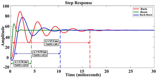
Figure 11.
Step response of the buck, boost, and buck-boost converter.
Figure 12 shows that the OS of the ĆUK converter is higher than the SEPIC converter. The OS presented by the ĆUK converter is 96.7%, while the OS performed by the SEPIC converter is 46%. Another method that can minimize the OS is to increase the bandwidth of the voltage loop, as the converter tends to respond quickly to the sudden change introduced in the input voltage. The ĆUK converter shows a better of 103 ms compared to 118 ms for the SEPIC converter. The summary of the step response of these converters is presented in Table 4.


Table 2.
Kyocera KC200GT specifications [,].
Table 2.
Kyocera KC200GT specifications [,].
| Parameters | Value |
|---|---|
| Maximum power () | 200 W |
| Cells per module | 54 |
| Open-circuit voltage () | 32.9 V |
| Short-circuit current () | 8.21 A |
| Maximum power voltage () | 26.3 V |
| Maximum power current () | 7.61 A |
| Voltage temperature coefficient | −0.123 V/C |
| Current temperature coefficient | 0.00318 A/C |

Table 3.
Simulation parameters.
Table 3.
Simulation parameters.
| Item | Buck | Boost | Buck-Boost | ĆUK | SEPIC |
|---|---|---|---|---|---|
| 0.7 | 3.33 | 2.33 | 2.33 | 2.33 | |
| ≥ 1.13 | ≥ 25.56 | ≥ 12.52 | ≥ 12.52 | ≥ 12.52 | |
| ≥ 84.75 H | ≥ 402.50 H | ≥ 402.50 H | ≥ 402.50 H | ≥ 402.5 H | |
| - | - | - | ≥ 402.50 H | ≥ 402.50 H | |
| ≥ 221.24 F | ≥ 273.89 F | ≥ 559.11 F | ≥ 685 F | ≥ 685 F | |
| - | - | - | ≥ 19.97 F | ≥ 559.11 F | |
| ≥ 1300 F | ≥ 108.70 F | ≥ 1300 F | ≥ 108.70 F | ≥ 108.70 F |

Table 4.
Step response of the converters reviewed.
Table 4.
Step response of the converters reviewed.
| Converter | Settling Time (ms) | Overshoot (%) |
|---|---|---|
| Buck | 17.1 | 69 |
| Boost | 1.76 | 23.5 |
| Buck-Boost | 9.79 | 47.1 |
| ĆUK | 103 | 46 |
| SEPIC | 118 | 96.7 |
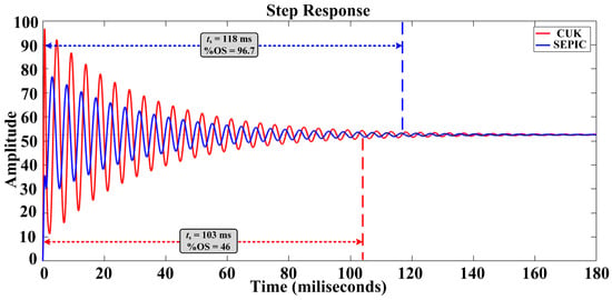
Figure 12.
Step response of the ĆUK and SEPIC converter.
The root locus shows the root of the closed-loop system’s characteristic equation to find the response of all values of a system parameter []. The root locus depicts the placements of the closed-loop poles as a function of the gain. If the gain alternates between zero and infinite gain, the placement of the closed-loop poles changes positions from the open-loop poles towards the open-loop zeros.
Figure 13 represents the root loci of buck, boost, and buck-boost converters. From the design perspective, the closed-loop poles represent the roots of the closed-loop system characteristic equation. Depending on the poles’ position, one can decide if the system is stable, unstable, or marginally stable [,,]. The poles of the buck and buck-boost converter appear near the origin and the real axis. The closed-loop system seems to be stable, as the roots of the closed-loop characteristic equation lie on the left-hand side of the axis for some of the gain values. Therefore, the boost converter design is stable, as its poles lie on the negative side of the s-plane. The system (i.e., for all three converters) is not unstable, as there is not a single pole on the positive half-plane. It can also be concluded that the buck and buck-boost converters are relatively less stable, as their poles lie near the imaginary axis compared to the boost converter, whose poles lie far from the imaginary axis.
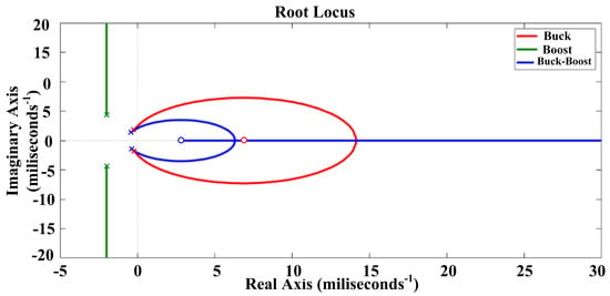
Figure 13.
Root loci of the buck, boost, and buck−boost converter.
Figure 14 illustrates the root loci of the ĆUK and SEPIC converters, which shows that both converters exhibit two right half-plane zeros. Since stable operation requires that all poles lie in the left half-plane of the complex plane, it is implied that the control system of these converters will be stable when installed in the PV system. However, two left half-plane zeros lie on the imaginary axis of these converters, indicating that if the PV system requires sampling of several distant operating points on its I-V curve, the stability and performance of the control system may deteriorate. Therefore, a complex control system may be needed to address this issue. Nevertheless, considering the position of the poles, these two converters are characterized as marginally stable, leading to what can be referred to as “limited stability”. The results indicate that the response and settling time of the boost converter is better compared to other converters when installed in the PV system. It is because of this reason that it falls in the category of nearly second-order converter and does not exhibit any pole or zero on the right-half plane of the pole-zero graph. Another important point is the low value of the capacitor, as the input supply from PV is continuous. The buck converter and buck-boost converter are stable under steady-state weather conditions. However, with varying weather conditions and perturbations in duty cycle for MPP tracking, the control system may undergo extensive transient periods, since these converters exhibit zero on the right-half plane of the pole-zero graph. Nevertheless, these two converters are better than ĆUK and SEPIC converters in terms of control, as they also fall in the second-order category. Both ĆUK and SEPIC converters take more setting time compared to basic converters. This is because they exhibit zeros in the right-half plane and also reductions in the higher-order category. From these results, it can be deduced that the gains of the ĆUK and SEPIC converters are higher compared to those of the boost converter. However, keeping in mind the low-order converter, better control, fast settling time, reasonable gain, and implementation ease, the PV designers prefer to use a boost converter in the PV system compared to other converters.
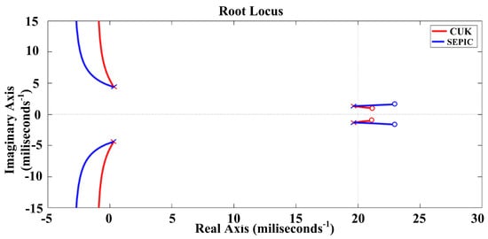
Figure 14.
Root loci of the ĆUK and SEPIC converter.
Figure 15, Figure 16, Figure 17, Figure 18 and Figure 19 demonstrate the simulation results when all the converters (buck, boost, buck-boost, ĆUK, and SEPIC) are exposed to changing atmospheric conditions. The component values computed in Table 3 are employed in the circuits where D = 0.7 and = 20 kHz. The simulations are carried out in the PSIM software, and the P&O algorithm is engaged in all the converters to ensure MPP achievement. The graphical representation of , , and D corresponding to irradiance condition changes is validated in Figure 15, Figure 16, Figure 17, Figure 18 and Figure 19.
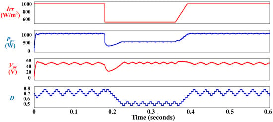
Figure 15.
Simulation results of the buck converter under changing atmospheric conditions.
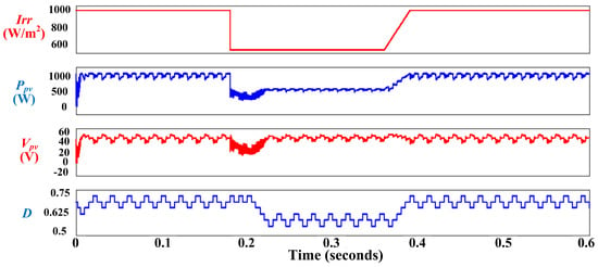
Figure 16.
Simulation results of the boost converter under changing atmospheric conditions.
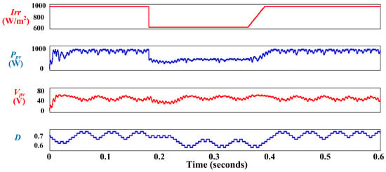
Figure 17.
Simulation results of the buck-boost converter under changing atmospheric conditions.
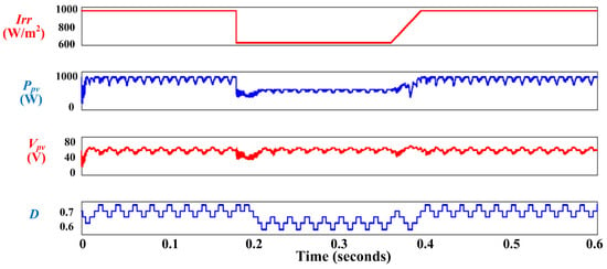
Figure 18.
Simulation results of the ĆUK converter under changing atmospheric conditions.
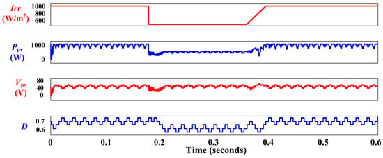
Figure 19.
Simulation results of the SEPIC converter under changing atmospheric conditions.
At t = 0 s, the irradiance level is 1000 , and the P&O algorithm starts tracking the MPP, which is 1200 W at the given irradiance condition. At t = 0.18 s, abruptly, the irradiance drops from 1000 to 500 due to clouds’ appearance in the sky. The available power from the PV array halves, and the P&O algorithm guarantees the extraction of the maximum available power. Initially, the response of all the converters is oscillatory due to the rapid variation in environmental conditions, but within a few ms, the steady state is attained. The pictorial behaviors of all the converters at 500 are illustrated in Figure 15, Figure 16, Figure 17, Figure 18 and Figure 19. At t = 0.36 s, the sunlight fights to recover, and the irradiance level spread reaches 1000 again. The converters’ outcomes are summarized in Table 5 under the above mentioned atmospheric conditions in terms of , , and D.

Table 5.
Summary of PV array output.
These results and Table 5 clearly indicate that, keeping in mind the control system implementation, converter installation, and MPP performance, the two conventional converters are the preferred choices. Since for most PV applications, a higher voltage is demanded at the output, the boost converter stands out as the best. For applications where both buck and boost modes are required in order to mitigate the partial-shading/mismatch effects in PV string, a buck-boost converter can be installed. Sometimes, when the PV arrays are installed with small-sized strings in order to reduce the partial shading/mismatch effects, a higher gain converter may be needed, and for these cases, CĆUK and SEPIC can be considered.
5. Conclusions
This paper reviews the modeling, designing, and implementation of buck, boost, buck-boost, ĆUK, and SEPIC converters. It also demonstrates the state-space average model through a general and intuitive deriving process, including several parameters and uncertainties. The switching effects on the state equations, system stability, and overall performance are shown for all converters. Optimal efficiency is observed in all converters as their dc gain gets close to unity. The output voltages of converters were acquired when PV panels operated with precipitously changing irradiation values. The non-isolated converters studied in this paper are of two types. The first one had one inductor and one capacitor other than the input capacitor; this type was referred to as Type 1, while the second one with more than one inductor and/or capacitor was referred to as Type 2. For type 1 dc-dc converters, the results revealed that the buck converter requires 84.75 μH compared to the 402.5 μH requirement for boost and buck-boost converter. Furthermore, the buck converter requires only a 221.4 μF output capacitor compared to 273.89 μF and 559.11 μF for boost and buck-boost converter. For Type 1 dc-dc converters, the lowest input capacitor requirement is for the boost converter. This requirement is 108.70 μF compared to the large input capacitance of 1300 μF for buck and buck-boost converters. In terms of th component values of Type 2 dc-dc converters, the Ćuk converter requirement of is almost 28 times less than that of a SEPIC converter. In terms of the step response performance, the boost converter requires the minimum time to settle down, followed by the buck converter, buck-boost, Ćuk and SEPIC. The boost converter also outperforms the other converters in terms of the percentage overshoot (OS) followed by Ćuk, buck-boost, buck, and then the SEPIC converter. It is perceived that the ĆUK and SEPIC converters’ OS and output value reach times are proximate to one another. Several uncertainties in dc-dc converters have been taken into account, including capacitance, inductance, and other variable conditions. This in-depth review presents a clear understanding and comparison of widely used dc-dc converters when choosing a specific application. The rendering of time-domain dynamic models is made easier using the state-space averaging approach for each of the listed dc-dc converters. The boost converter outperforms all other converters in terms of stability, settling time, and overshoot. This is primarily due to the presence of only one time-varying parameter in a boost converter. Additionally, the boost converter has input inductance, which ensures a continuous input current. Note that the input current is discontinuous in the buck converter, and in the buck-boost converter for which a large input capacitor is required. The ĆUK and SEPIC converters have a greater number of components and, therefore, they also are outclassed by the boost converter in terms of the abovementioned attributes. Further, the dc-dc boost converters do not require a blocking diode in battery-charging applications. The only shortfall of the state-space model is its inability to simulate the ripple effect on the inductor current and output voltage, as the frequency switching input element is not present.
This work presents the research findings about the five fundamental power electronics dc-dc converters. By utilizing the features of advanced control techniques such as model-predictive control, artificial-intelligence techniques, and control optimization methods, the issues of converter, especially ĆUK and SEPIC, can be minimized. This research work may also help the researcher to model and evaluate the performance and stability of isolated converters for a PV system.
Author Contributions
Conceptualization, A.F.M. and M.U.K.; methodology, A.F.M.; software, H.A.S.; validation, M.U.K., A.M.N. and M.Z.; formal analysis, A.F.M.; investigation, M.Z.; resources, A.M.N.; data curation, A.F.M.; writing—original draft preparation, H.A.S.; writing—review and editing, A.F.M., H.A.S.; visualization, M.U.K.; supervision, A.F.M.; project administration, A.F.M.; funding acquisition, A.M.N. All authors have read and agreed to the published version of the manuscript.
Funding
This study is supported via funding from Prince Sattam bin Abdulaziz University project number (PSAU/2023/R/1445).
Institutional Review Board Statement
Not applicable.
Informed Consent Statement
Not applicable.
Data Availability Statement
No new data were created or analyzed in this study. Data sharing is not applicable to this article.
Conflicts of Interest
The authors declare no conflict of interest.
References
- Ahmed, S.; Mekhilef, S.; Mubin, M.; Tey, K.S.; Kermadi, M. An enhanced scanning technique for flexible power point tracking under partial shading condition. Sol. Energy 2023, 262, 111817. [Google Scholar] [CrossRef]
- Ghodusinejad, M.H.; Ghodrati, A.; Zahedi, R.; Yousefi, H. Multi-criteria modeling and assessment of PV system performance in different climate areas of Iran. Sustain. Energy Technol. Assess. 2022, 53, 102520. [Google Scholar] [CrossRef]
- Khah, M.V.; Zahedi, R.; Eskandarpanah, R.; Mirzaei, A.M.; Farahani, O.N.; Malek, I.; Rezaei, N. Optimal sizing of residential photovoltaic and battery system connected to the power grid based on the cost of energy and peak load. Heliyon 2023, 9, e14414. [Google Scholar] [CrossRef]
- Rizvi, A.A.; Sher, H.A.; Addoweesh, K.E.; El-Leathy, A.; Al-Ansary, H.; Al-Haddad, K. Simulation of sun tracking system for point focus fresnel collector. In Proceedings of the 2017 IEEE 26th International Symposium on Industrial Electronics (ISIE), Edinburgh, UK, 19–21 June 2017; pp. 1023–1028. [Google Scholar]
- Katche, M.L.; Makokha, A.B.; Zachary, S.O.; Adaramola, M.S. A comprehensive review of maximum power point tracking (mppt) techniques used in solar pv systems. Energies 2023, 16, 2206. [Google Scholar] [CrossRef]
- Sah, B.; Kumar, G.V.E.S. A comparative study of different MPPT techniques using different dc-dc converters in a standalone PV system. In Proceedings of the 2016 IEEE Region 10 Conference (TENCON), Singapore, 22–25 November 2016; pp. 1690–1695. [Google Scholar]
- Shaikh, A.M.; Shaikh, M.F.; Shaikh, S.A.; Krichen, M.; Rahimoon, R.A.; Qadir, A. Comparative analysis of different MPPT techniques using boost converter for photovoltaic systems under dynamic shading conditions. Sustain. Energy Technol. Assess. 2023, 57, 103259. [Google Scholar]
- Hossain, M.; Rahim, N. Recent progress and development on power DC-DC converter topology, control, design and applications: A review. Renew. Sustain. Energy Rev. 2018, 81, 205–230. [Google Scholar] [CrossRef]
- Tan, S.C.; Lai, Y.M.; Chi, K.T. General design issues of sliding-mode controllers in DC–DC converters. IEEE Trans. Ind. Electron. 2008, 55, 1160–1174. [Google Scholar]
- Perry, A.G.; Feng, G.; Liu, Y.F.; Sen, P.C. A design method for PI-like fuzzy logic controllers for DC–DC converter. IEEE Trans. Ind. Electron. 2007, 54, 2688–2696. [Google Scholar] [CrossRef]
- Forsyth, A.; Mollov, S. Modelling and control of DC-DC converters. Power Eng. J. 1998, 12, 229–236. [Google Scholar] [CrossRef]
- Tan, R.H.; Hoo, L.Y. DC-DC converter modeling and simulation using state space approach. In Proceedings of the 2015 IEEE Conference on Energy Conversion (CENCON), Johor Bahru, Malaysia, 19–20 October 2015; pp. 42–47. [Google Scholar]
- Priewasser, R.; Agostinelli, M.; Unterrieder, C.; Marsili, S.; Huemer, M. Modeling, control, and implementation of DC–DC converters for variable frequency operation. IEEE Trans. Power Electron. 2013, 29, 287–301. [Google Scholar] [CrossRef]
- Ghodusinejad, M.H.; Noorollahi, Y.; Zahedi, R. Optimal site selection and sizing of solar EV charge stations. J. Energy Storage 2022, 56, 105904. [Google Scholar] [CrossRef]
- Liu, X.; Qiu, L.; Fang, Y.; Wang, K.; Li, Y.; Rodríguez, J. Predictive Control of Voltage Source Inverter: An Online Reinforcement Learning Solution. IEEE Trans. Ind. Electron. 2023, 54, 495–503. [Google Scholar] [CrossRef]
- Liu, X.; Qiu, L.; Fang, Y.; Wang, K.; Li, Y.; Rodríguez, J. Finite control-set learning predictive control for power converters. IEEE Trans. Ind. Electron. 2023, 2023, 1–7. [Google Scholar] [CrossRef]
- Guesmi, K.; Hamzaoui, A. On the modelling of DC-DC converters: An enhanced approach. Int. J. Numer. Model. Electron. Netw. Devices Fields 2011, 24, 36–57. [Google Scholar] [CrossRef]
- Lehman, B.; Bass, R.M. Switching frequency dependent averaged models for PWM DC-DC converters. IEEE Trans. Power Electron. 1996, 11, 89–98. [Google Scholar] [CrossRef]
- Hussain, A.; Sher, H.A.; Murtaza, A.F.; Al-Haddad, K. Improved voltage controlled three phase voltage source inverter using model predictive control for standalone system. In Proceedings of the IECON 2018—44th Annual Conference of the IEEE Industrial Electronics Society, Washington, DC, USA, 21–23 October 2018; pp. 5308–5313. [Google Scholar]
- Guan, Y.; Wang, Y.; Wang, W.; Xu, D. Analysis and design of a high-frequency DC/DC converter based on a resonant rectifier. IEEE Trans. Ind. Electron. 2017, 64, 8492–8503. [Google Scholar] [CrossRef]
- Hasanpour, S.; Baghramian, A.; Mojallali, H. Analysis and modeling of a new coupled-inductor buck–boost DC–DC converter for renewable energy applications. IEEE Trans. Power Electron. 2019, 35, 8088–8101. [Google Scholar] [CrossRef]
- Chen, X.; Chen, Y.; Zhang, B.; Qiu, D. A modeling and analysis method for fractional-order DC–DC converters. IEEE Trans. Power Electron. 2016, 32, 7034–7044. [Google Scholar] [CrossRef]
- Levis, C.; O’Loughlin, C.; O’Donnell, T.; Hill, M. A comprehensive state-space model of two-stage grid-connected PV systems in transient network analysis. Int. J. Electr. Power Energy Syst. 2019, 110, 441–453. [Google Scholar] [CrossRef]
- Mumtaz, F.; Yahaya, N.Z.; Meraj, S.T.; Singh, B.; Kannan, R.; Ibrahim, O. Review on non-isolated DC-DC converters and their control techniques for renewable energy applications. Shams Eng. J. 2021, 12, 3747–3763. [Google Scholar] [CrossRef]
- Rim, C.T.; Joung, G.B.; Cho, G.H. Practical switch based state-space modeling of DC-DC converters with all parasitics. IEEE Trans. Power Electron. 1991, 6, 611–617. [Google Scholar] [CrossRef][Green Version]
- Azer, P.; Emadi, A. Generalized state space average model for multi-phase interleaved buck, boost and buck-boost DC-DC converters: Transient, steady-state and switching dynamics. IEEE Access 2020, 8, 77735–77745. [Google Scholar] [CrossRef]
- Ghanbari, N.; Shabestari, P.M.; Mehrizi-Sani, A.; Bhattacharya, S. State-space modeling and reachability analysis for a dc microgrid. In Proceedings of the 2019 IEEE Applied Power Electronics Conference and Exposition (APEC), Virtual, 17–21 March 2019; pp. 2882–2886. [Google Scholar]
- Chewale, M.A.; Wanjari, R.A.; Savakhande, V.B.; Sonawane, P.R. A review on isolated and non-isolated DC-DC converter for PV application. In Proceedings of the 2018 International Conference on Control, Power, Communication and Computing Technologies (ICCPCCT), Kannur, India, 23–24 March 2018; pp. 399–404. [Google Scholar]
- Patel, B.D.; Rana, A. A pole-placement approach for buck converter based PV array Emulator. In Proceedings of the 2016 IEEE 1st International Conference on Power Electronics, Intelligent Control and Energy Systems (ICPEICES), Delhi, India, 4–6 July 2016; pp. 1–5. [Google Scholar]
- Darbali-Zamora, R.; Ortiz-Rivera, E.I. A State Space Average Model for Dynamic Microgrid Based Space Station Simulations. In Proceedings of the 2017 IEEE 44th Photovoltaic Specialist Conference (PVSC), Washington, DC, USA, 25–30 June 2017; pp. 2957–2962. [Google Scholar]
- Yao, J.; Zheng, K.; Abramovitz, A. Small-signal model of switched inductor boost converter. IEEE Trans. Power Electron. 2018, 34, 4036–4040. [Google Scholar] [CrossRef]
- Zhang, W.; Tan, X.; Wang, K.; Li, T.; Chen, J. Design for boost DC-DC converter controller based on state-space average method. Integr. Ferroelectr. 2016, 172, 152–159. [Google Scholar] [CrossRef]
- Duong, M.Q.; Sava, G.N.; Scripcariu, M.; Mussetta, M. Design and simulation of PI-type control for the Buck Boost converter. In Proceedings of the 2017 International Conference on Energy and Environment (CIEM), Bucharest, Romania, 19–20 October 2017; pp. 79–82. [Google Scholar]
- Cuk, S.M.; Middlebrook, R.D. DC-to-DC Switching Converter. US Patent 4,184,197, 28 September 1980. [Google Scholar]
- Darwish, A.; Holliday, D.; Ahmed, S.; Massoud, A.M.; Williams, B.W. A single-stage three-phase inverter based on Cuk converters for PV applications. IEEE J. Emerg. Sel. Top. Power Electron. 2014, 2, 797–807. [Google Scholar] [CrossRef]
- Chiang, S.; Shieh, H.J.; Chen, M.C. Modeling and control of PV charger system with SEPIC converter. IEEE Trans. Ind. Electron. 2008, 56, 4344–4353. [Google Scholar] [CrossRef]
- Kircioğlu, O.; Ünlü, M.; Camur, S. Modeling and analysis of DC-DC SEPIC converter with coupled inductors. In Proceedings of the 2016 International Symposium on Industrial Electronics (INDEL), Banja Luka, Bosnia and Herzegovina, 3–5 November 2016; pp. 1–5. [Google Scholar]
- Taghvaee, M.; Radzi, M.; Moosavain, S.; Hizam, H.; Marhaban, M.H. A current and future study on non-isolated DC–DC converters for photovoltaic applications. Renew. Sustain. Energy Rev. 2013, 17, 216–227. [Google Scholar] [CrossRef]
- Verma, M.; Kumar, S.S. Hardware design of sepic converter and its analysis. In Proceedings of the 2018 International Conference on Current Trends towards Converging Technologies (ICCTCT), Coimbatore, India, 1–3 March 2018; pp. 1–4. [Google Scholar]
- Babaei, E.; Mahmoodieh, M.E.S. Calculation of output voltage ripple and design considerations of SEPIC converter. IEEE Trans. Ind. Electron. 2013, 61, 1213–1222. [Google Scholar] [CrossRef]
- Seguel, J.L.; Seleme, S.I., Jr.; Morais, L.M. Comparative study of Buck-Boost, SEPIC, Cuk and Zeta DC-DC converters using different MPPT methods for photovoltaic applications. Energies 2022, 15, 7936. [Google Scholar] [CrossRef]
- Panigrahi, R.; Mishra, S.K.; Joshi, A.; Ngo, K.D. DC-DC converter synthesis: An inverse problem. IEEE Trans. Power Electron. 2020, 35, 12633–12638. [Google Scholar] [CrossRef]
- Erickson, R.W.; Maksimovic, D. Fundamentals of Power Electronics; Springer Science & Business Media: Berlin/Heidelberg, Germany, 2007. [Google Scholar]
- Ned, M.; Ullmann, F.; Robbins, W. Power Electronics; Wiley: Hoboken, NJ, USA, 2003. [Google Scholar]
- Xiao, W.; Ozog, N.; Dunford, W.G. Topology study of photovoltaic interface for maximum power point tracking. IEEE Trans. Ind. Electron. 2007, 54, 1696–1704. [Google Scholar] [CrossRef]
- Xiao, W. Photovoltaic Power System: Modeling, Design, and Control; John Wiley & Sons: Hoboken, NJ, USA, 2017. [Google Scholar]
- Datasheet Kyocera KC200GT. Available online: https://www.datasheets.com/en/part-details/kc200gt-kyocera62747508 (accessed on 7 August 2023).
- Solanki, C.S. Solar Photovoltaics: Fundamentals, Technologies and Applications; Phi Learning Pvt. Ltd.: New Delhi, India, 2015. [Google Scholar]
- Nadeem, A.; Sher, H.A.; Murtaza, A.F.; Ahmed, N.; Al-Durra, A. An improved sliding mode control–based GMPPT algorithm for photovoltaic system. Trans. Inst. Meas. Control 2023, 45, 1726–1737. [Google Scholar] [CrossRef]
- Shan, Z.; Tan, S.C.; Chi, K.T. Transient mitigation of dc–dc converters for high output current slew rate applications. IEEE Trans. Power Electron. 2012, 28, 2377–2388. [Google Scholar] [CrossRef][Green Version]
- Zhen, S.; Zeng, P.; Chen, J.; Zhou, W.; Wang, J.; Luo, P.; Zhang, B. Transient response improvement of DC-DC converter by current mode variable on time control. In Proceedings of the 2018 IEEE 61st International Midwest Symposium on Circuits and Systems (MWSCAS), Windsor, ON, Canada, 5–8 August 2018; pp. 603–606. [Google Scholar][Green Version]
- Villalva, M.G.; Gazoli, J.R.; Ruppert Filho, E. Comprehensive approach to modeling and simulation of photovoltaic arrays. IEEE Trans. Power Electron. 2009, 24, 1198–1208. [Google Scholar] [CrossRef]
- Murtaza, A.F.; Sher, H.A.; Khan, F.U.; Nasir, A.; Spertino, F. Efficient mpp tracking of photovoltaic (pv) array through modified boost converter with simple smc voltage regulator. IEEE Trans. Sustain. Energy 2022, 13, 1790–1801. [Google Scholar] [CrossRef]
- Shen, Y.; Chen, M.; Majji, M.; Skelton, R.E. Q-Markov Covariance equivalent realizations for unstable and marginally stable systems. Mech. Syst. Signal Process. 2023, 196, 110343. [Google Scholar] [CrossRef]
- Levine, W.S. Control System Fundamentals; CRC Press: Boca Raton, FL, USA, 1999. [Google Scholar]
- Hussain, A.; Sher, H.A.; Murtaza, A.F.; Al-Haddad, K. A novel sensor-less current technique for photovoltaic system using DC transformer model based model predictive control. Int. J. Electr. Power Energy Syst. 2020, 122, 106165. [Google Scholar] [CrossRef]
Disclaimer/Publisher’s Note: The statements, opinions and data contained in all publications are solely those of the individual author(s) and contributor(s) and not of MDPI and/or the editor(s). MDPI and/or the editor(s) disclaim responsibility for any injury to people or property resulting from any ideas, methods, instructions or products referred to in the content. |
© 2023 by the authors. Licensee MDPI, Basel, Switzerland. This article is an open access article distributed under the terms and conditions of the Creative Commons Attribution (CC BY) license (https://creativecommons.org/licenses/by/4.0/).