Article

An Improved Modulation Method for Suppressing High Frequency Common-Mode Voltage in SiC Motor Drive System

State Key Laboratory of Power Transmission Equipment & System Security and New Technology, Chongqing University, Chongqing 400044, China
*
Author to whom correspondence should be addressed.
World Electr. Veh. J. 2021, 12(3), 111; https://doi.org/10.3390/wevj12030111
Submission received: 16 July 2021 / Revised: 3 August 2021 / Accepted: 5 August 2021 / Published: 8 August 2021

Abstract

:
High-frequency common-mode voltage generated by inverters causes severe negative effects, particularly in silicon carbide (SiC) Metal-Oxide-Semiconductor Field-Effect Transistors (MOSFETs)-driven motors. Additionally, common suppression strategies would increase hardware expenses or sacrifice the switching speed of SiC devices. This article proposes an improved no-zero vector modulation strategy to suppress high-frequency common-mode voltage without increasing the cost of hardware. In this method, only nonzero vectors are utilized to reduce common-mode voltage. Firstly, the influence of different switching states on the characteristics of SiC MOSFETs has been studied by double-pulse tests, which explains why zero vectors will cause more serious voltage oscillations. Secondly, common-mode voltage suppression failure caused by the high-frequency dead zone effect has been analyzed in detail. Based on traditional Active Zero State Pulse Width Modulation (AZSPWM), complementary device conduction logic and dead-zone compensation methods are proposed. In switching moments, different turn-on logic is selected to ensure that only one switch acts, and different dead zone compensation methods are selected to deal with the common-mode suppression failure, which effectively avoids high-frequency common-mode voltage spikes. Finally, simulation and experimental results verify that the improved modulation algorithm can effectively suppress high-frequency common-mode voltage.

1. Introduction

Silicon carbide devices have unparalleled advantages in high-frequency and high-power-density applications due to their fast switching speed, high voltage level withstood, and high working temperature, which are designed to improve the efficiency and power density of motor drive systems [1,2]. However, due to the faster switching speed of SiC MOSFETs, the switching transient oscillation is much more serious than that of Si devices, causing electromagnetic compatibility problems to be more serious than those of traditional motor drive systems. Studies have shown that high-frequency common-mode voltage generated by PWM inverters is the main reason for the problems related to EMI in the motor drive system [3]. Therefore, to solve the problems such as EMI in SiC motor drive system, it is necessary to effectively suppress high-frequency common-mode voltage.
Common-mode voltage suppression methods are generally divided into passive suppression [4,5,6] and active suppression [7,8,9,10,11,12,13,14,15,16]. Passive suppression methods reduce common-mode output by adding passive components in the circuit such as common-mode inductors [4] or passive filters [5,6]. Although passive suppression methods can suppress common-mode voltage and its negative effects to a certain extent, they increase the hardware cost and volume. Active suppression methods include inserting an active filter in the circuit [7], adopting a three-phase four-leg converter [8], or changing the inverter control algorithm [9,10,11,12,13,14,15,16]. To overcome the overvoltage problem of AZSPWM and the limited operating range of NSPWM, a modified AZSPWM and a hybrid algorithm have been proposed in [9]. Reference [9] verified that common-mode voltage can be effectively suppressed under AZSPWM and Near State Pulse Width Modulation (NSPWM), but the influence of dead zone effect on the common-mode voltage is neglected. In addition, the adverse effects of these modulation techniques, e.g., more severe current ripple for AZSPWM [9], have not been discussed for a SiC-based inverter. In reference [10], the influence of dead zone on the common-mode voltage of AZSPWM is analyzed, but only dead zone compensation is carried out for the failure of one of the two effective switching vectors. In reference [11], common-mode chokes and AZSPWM are used to suppress high-frequency common-mode voltage, but the parameter design of common-mode chokes depends on system parasitic parameters, and the value is difficult to determine. These PWM techniques reduce the amplitude of common-mode voltage by cutting back the use of zero vectors. Among the effective modulation techniques for common-mode voltage reduction, AZSPWM in [9] and tri-state pulse width modulation (TSPWM) in [14] are relatively easy to implement. Without utilizing the zero voltage vectors, active zero-state PWM (AZSPWM1, AZSPWM2, and AZSPWM3), remote-state PWM (RSPWM1, RSPWM2, and RSPWM3), and near-state PWM (NSPWM) have been investigated [15], [16]. However, the output waveforms quality is poor when using these methods, especially at a low modulation index. It can be seen that there is a lack of comprehensive systematic research on high-frequency common-mode voltage in SiC motor drive systems.
This paper analyzes common-mode voltage and evaluates and modifies the corresponding suppression method in SiC-based inverters for electric vehicle (EV) applications. In Section 2, double pulse tests of a three-phase full-bridge SiC inverter connected with motor load are carried out to study the influence of different switching states on the characteristics of SiC devices. Double pulse tests results reveal the law of high-frequency voltage oscillation, and based on the test results, no-zero vector modulation is selected to suppress high-frequency common-mode voltage. In Section 3, the conduction logic and dead zone effect of traditional AZSPWM at high switching frequency are analyzed in detail. On the basis of traditional AZSPWM, a set of complementary device conduction logic and dead zone compensation methods are added. In sector switching moments, different turn-on logic is selected to ensure that only one switch acts to avoid the common-mode voltage spike, and different dead zone compensation methods are selected to deal with the common-mode suppression failure caused by different switches. The commutation logic and action time of improved AZSPWM are given in the form of a table. Section 4 presents the simulation and experimental verification, and conclusions are drawn in Section 5.

2. Influence of Voltage Vectors on the Switching Performance of SiC devices

2.1. Definition of Common-Mode Voltage

The typical structure of a two-level three-phase voltage source inverter is shown in Figure 1. According to the definition, common-mode voltage U n g is the voltage between load neutral point n and grounding point g, U n g = U n o + U o g , considering that U o g is relatively small and changes slowly, U o g can be ignored, and U n o is used to approximate the common-mode voltage of the system:
U n o U a o + U b o + U c o 3
U a o , U b o , U c o is the voltage between a, b, c and the neutral point o of the capacitor, respectively.
The corresponding common-mode voltage value when each switch vector acts is shown in Table 1. Under conventional PWM modulation, common-mode voltage generated by the three-phase two-level inverter is a four-step wave jumping between ± V d c / 2 and ± V d c / 6 .

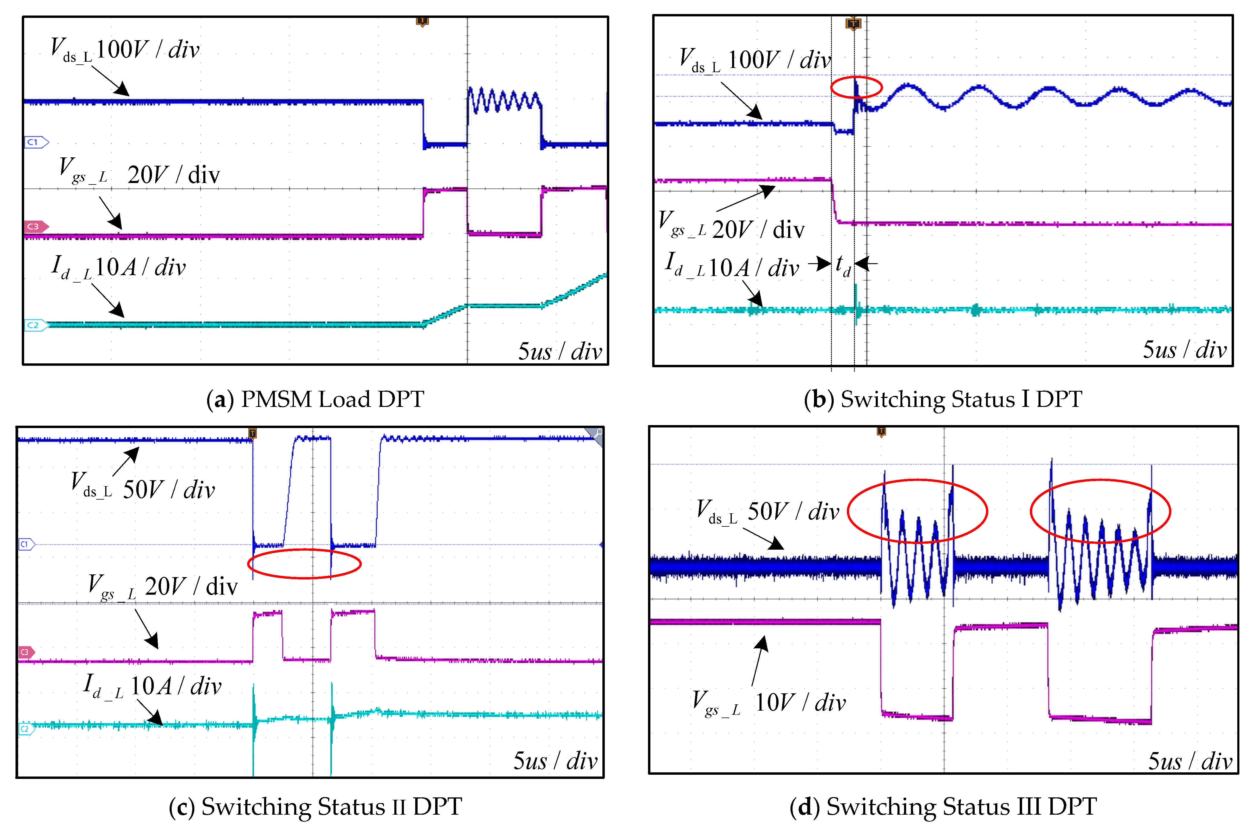
2.2. Double Pulse Test of SiC Three-Phase Full Bridge

Double pulse test (DPT) is a widely accepted method for evaluating the characteristics of semiconductor switches. However, in three-phase inverter of a PWM motor drive, the switching performance of SiC devices is always worse than the double pulse test results, which is manifested as slower switching speed, larger switching loss, and more serious ringing. Therefore, a simple double pulse test with load inductance is not enough to represent the actual situation of the inverter in the motor drive system. In order to fully utilize the potential advantages of SiC devices in motor drive systems, this paper systematically evaluates the switching characteristics of three-phase SiC inverter devices with motor loads. First, the eight switching vectors are classified according to the common-mode voltage amplitude in Table 1: I (100, 010, 001), II (110, 101, 011), and III (000, 111). Then, the switching characteristics of the SiC devices are tested under motor load, switching state I, switching state II, and switching state III, respectively, as shown in Figure 2.
The test results in Figure 3a show that at the turn-on moment, the drain-source voltage V d s of the tested SiC device does not have a voltage spike when a motor load is connected to the half bridge. However, in a three-phase full bridge circuit, as Figure 3b–d indicates, with the changes of phase B and phase C switching states, the higher the amplitude of the common-mode voltage is, the more severe the high-frequency voltage oscillates (d > c > b). In zero vector states, the common-mode voltage is the highest, and the voltage oscillation is the most serious. The approximate formula U n o ( U a o + U b o + U c o ) / 3 demonstrates that high-frequency drain-source voltage oscillation generated by SiC devices during the switching process will lead to high-frequency common-mode voltage oscillation and eventually aggravate a series of negative effects such as electromagnetic interference.

3. High-Frequency Common-Mode Voltage Suppression Strategy

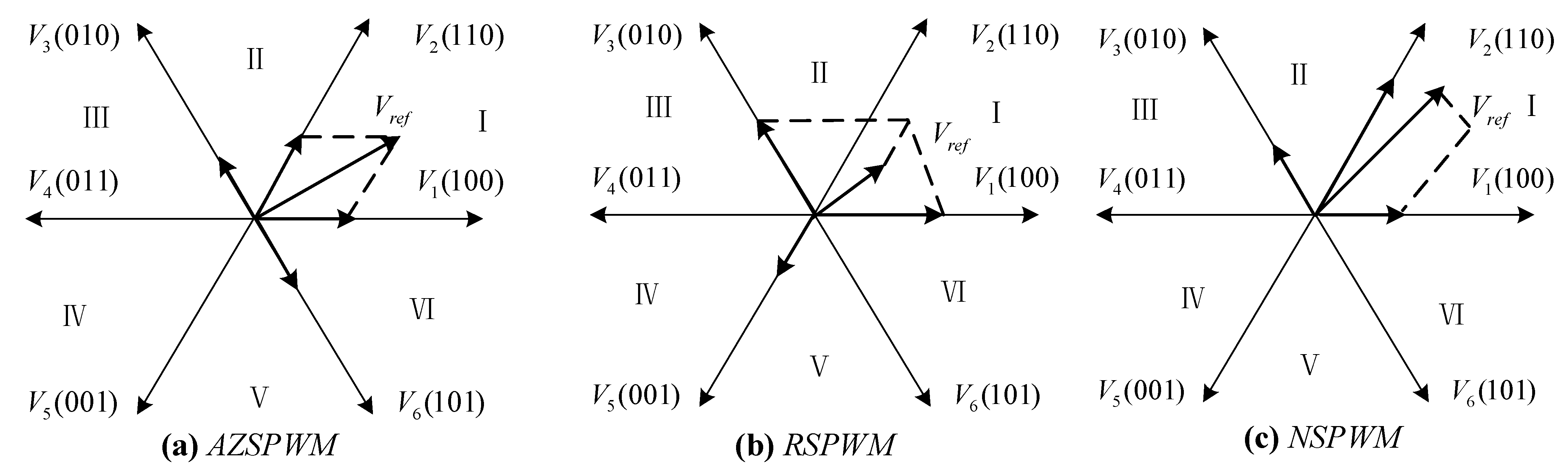
3.1. Reduced Common-Mode Voltage PWM

In a two-level PWM inverter, the amplitude of common-mode voltage generated by the zero vector is ± V d c / 2 , and the amplitude of the common-mode voltage is ± V d c / 6 when the non-zero vector is applied. Through the double pulse tests in the previous section, it is found that under the action of zero vectors, the leakage-source voltage oscillation of SiC devices will be more serious in the switching process, thus aggravating the high-frequency oscillation of common-mode voltage. Therefore, one idea to suppress high-frequency common-mode voltage is to avoid using zero vectors.
The peak value of common-mode voltage can be reduced by 66.7% by using only six other effective vectors instead of zero vectors. According to the effective vector used, the suppression common-mode voltage PWM can be divided into three categories: active zero state PWM (AZSPWM), remote state PWM (RSPWM), and near state PWM (NSPWM). Taking the reference voltage in the first sector as an example, the combination modes of the reference voltage vector under three kinds of no-zero vectors modulation are shown in Figure 4.
Since the use of zero vectors is avoided, all three modulation methods can reduce the common-mode voltage amplitude from ± V d c / 2 to ± V d c / 6 . However, AZSPWM will cause the problem of simultaneous operation of two-phase switches, which will further cause the line voltage polarity to jump rapidly. RSPWM and NSPWM will be limited by the modulation range, and the output line voltage will be distorted, which will cause phase current distortion. In practical applications, all three modulation methods exist: common-mode voltage spikes caused by the dead-time effect and sector jump, and motor-side overvoltage caused by rapid line voltage polarity jumps. In order to avoid being restricted by the linear modulation range, this article focuses on the analysis and improvement of the traditional AZSPWM.

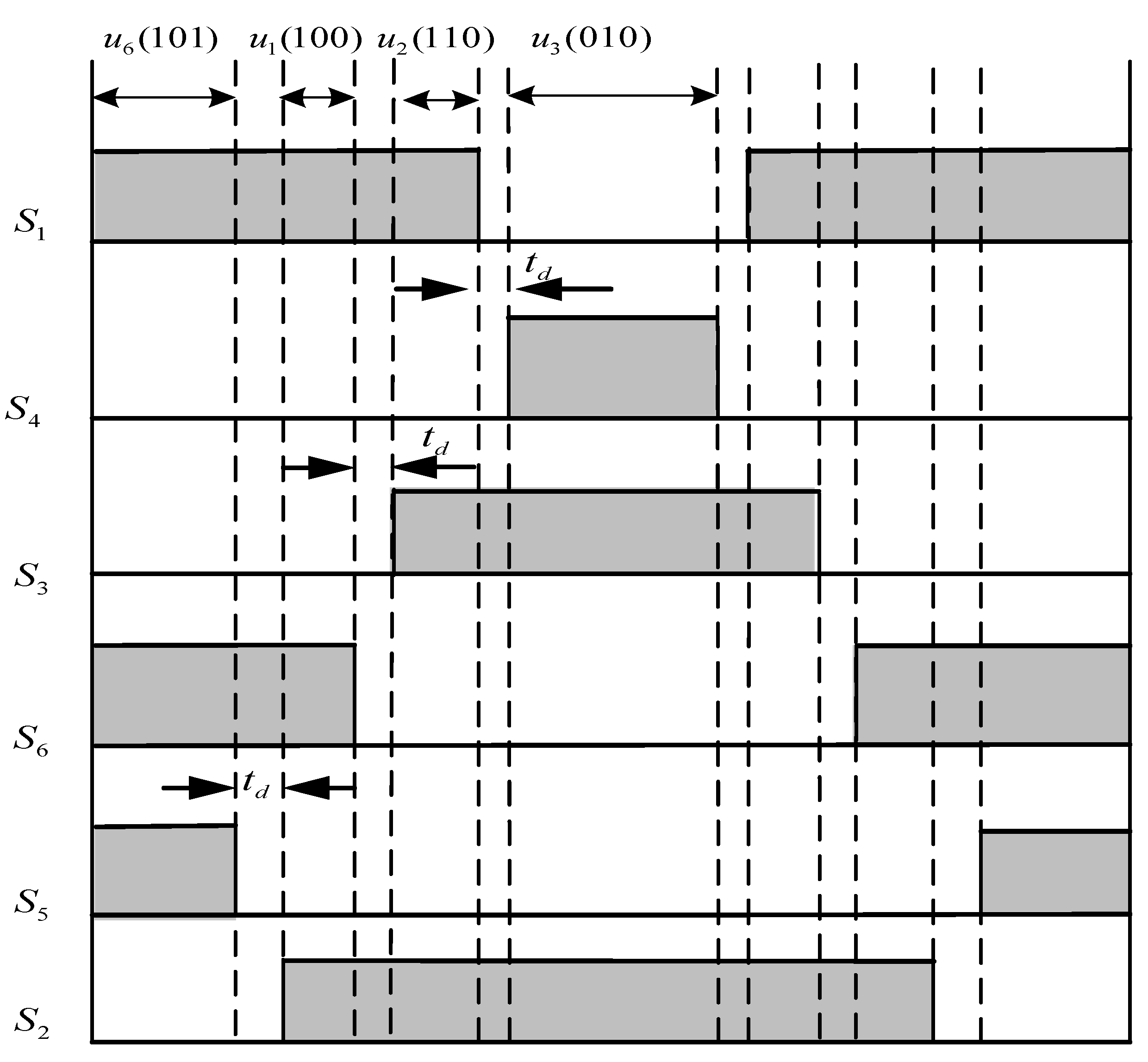
3.2. Dead-Zone Effect under High Switching Frequency

AZSPWM chooses two voltage vectors with 180° difference to replace zero vectors, so that the amplitude of common-mode voltage can be suppressed. Taking the reference voltage in sector I as an example, the order of reference voltage vector synthesis is U 6 U 1 U 2 U 3 U 2 U 1 U 6 , and the conduction logic sequence of the inverter is shown in Figure 5. According to the principle of volt-second balance, the relationship is as follows:
U 1 T 1 + U 2 T 2 + U 3 T 3 + U 6 T 6 = U r e f T s
T 1 + T 2 + T 3 + T 6 = T s
When the reference voltage vector position angle θ r is between 0 and π/6, if t 2 < 2 t d and t 1 > 2 t d , there will be a dead zone overlap area between the inverter output voltage u a o and u b o . In this area, if i a and i b are greater than zero at the same time, u a o and u b o will be clamped on the negative pole of the DC bus. At this time, u c o is also on the negative pole of the DC bus, so a voltage spike of V d c / 2 will appear in common-mode voltage output, and the suppression algorithm becomes invalid.
When the reference voltage vector position angle θ r is between π/6 and π/3, if t 1 < 2 t d and t 2 > 2 t d , there will be a dead zone overlap area between the inverter output voltage u b o and u c o . In this area, if i b and i c are smaller than zero at the same time, u b o and u c o will be clamped on the positive pole of the DC bus. At this time, u a o is also on the positive pole of the DC bus, so a voltage spike of V d c / 2 will appear in common-mode voltage output, and the suppression algorithm becomes invalid.
In summary, under high switching frequency, there is a working interval where the modulation algorithm fails at the moment of sector switching. In order to ensure that the common-mode voltage suppression algorithm is always effective, the modulation algorithm needs to be modified.

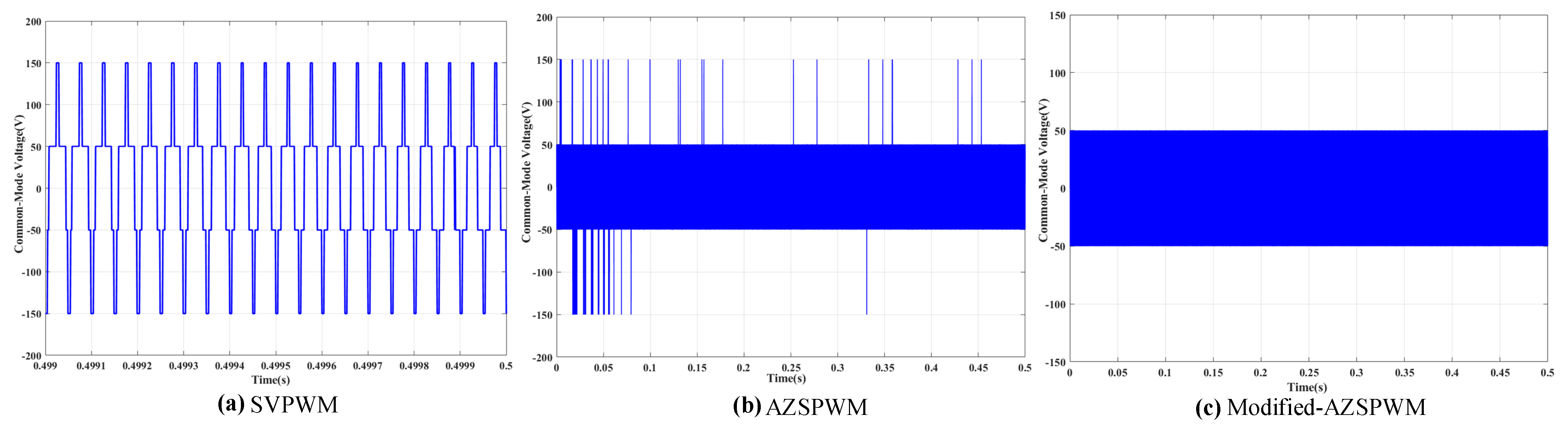
3.3. Modified Active Zero State PWM

It can be seen from the analysis in Section 3.2 that under high switching frequency, taking the reference voltage vector located in the first sector as an example, when the action time of an effective voltage vector V 1 , V 2 is less than the dead time or the reference voltage vector switches from sector I to sector II (switching state changing from {101} to {011}), failure of common-mode voltage suppression may occur, and common-mode voltage spikes may emerge. In order to avoid common-mode voltage spikes under high switching frequencies, this article proposes the following improvement measures on the basis of AZSPWM:
To eliminate the common-mode voltage spikes appearing in the sector conversion process, a complementary switching logic is proposed. Without changing the duty cycle time, switching logic Type I inverts the gate signals generated by T m a x and T m i n   , respectively, and keeps the gate signal generated by T m i d ; switching logic Type II inverts the gate signal generated by T m i d , and keep the gate signal generated by T m a x and T m i n . Type I and II constitute complementary conduction logic and the timing diagram is shown in Figure 6a.
To avoid the suppression failure caused by the dead zone effect, a compensation strategy is proposed. Taking the reference voltage vector in sector I as an example, on the basis of keeping volt-second balance, if V 1 action time is less than the dead zone, the compensation I will be performed according to the vector synthesis method in Figure 6b; if V 2 action time is less than the dead zone, the compensation II will be performed according to the vector synthesis method in Figure 6c. Additionally, other sectors can be deduced by analogy.
The optimized switching logic and action time are shown in Table 2, where X = 3 T s u β U d c   Y = 3 T s U d c ( 3 2 u α + 1 2 u β )   Z = 3 T s U d c ( 3 2 u α + 1 2 u β ) and μə and μβ are the components of the reference voltage vector on the axis α-β

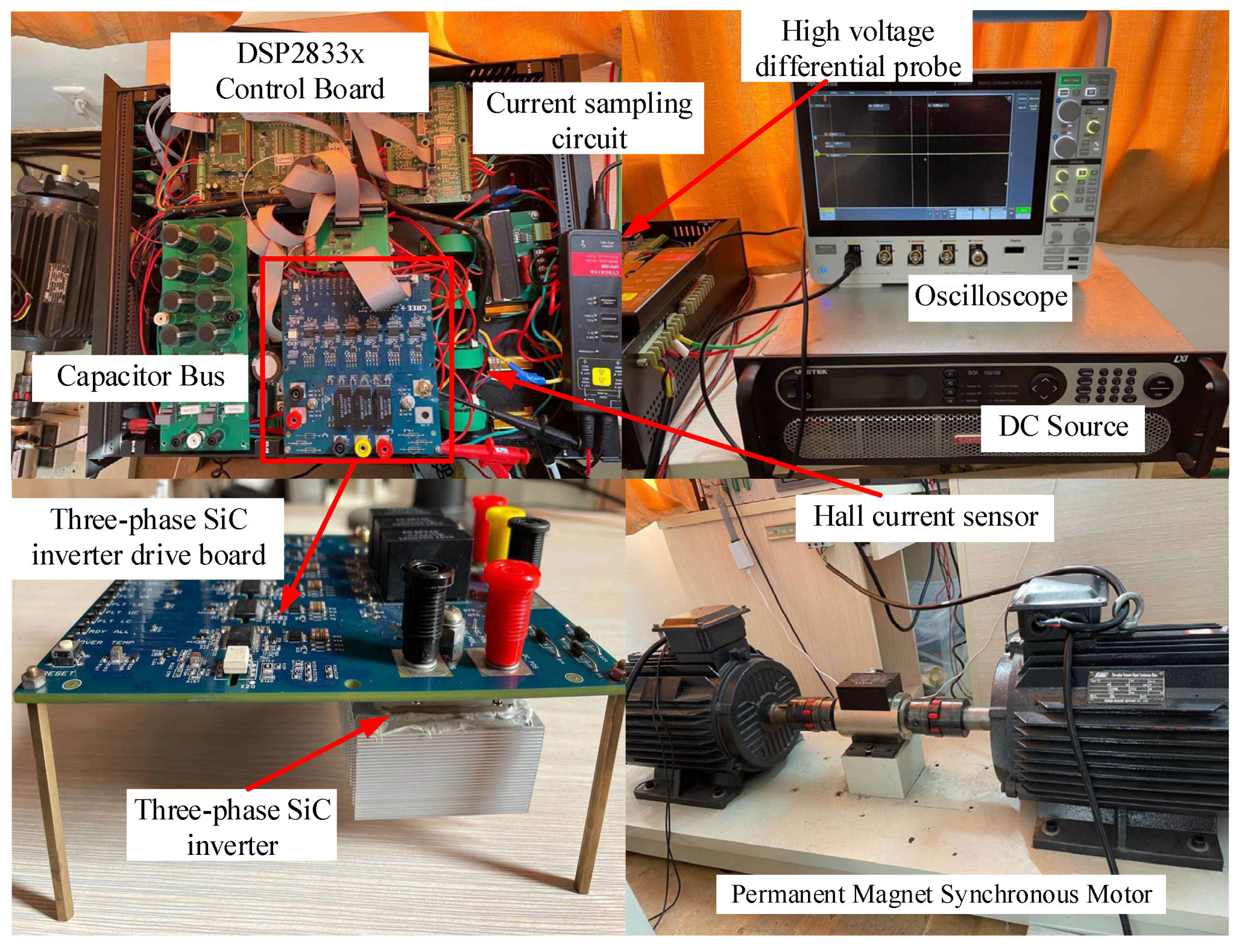
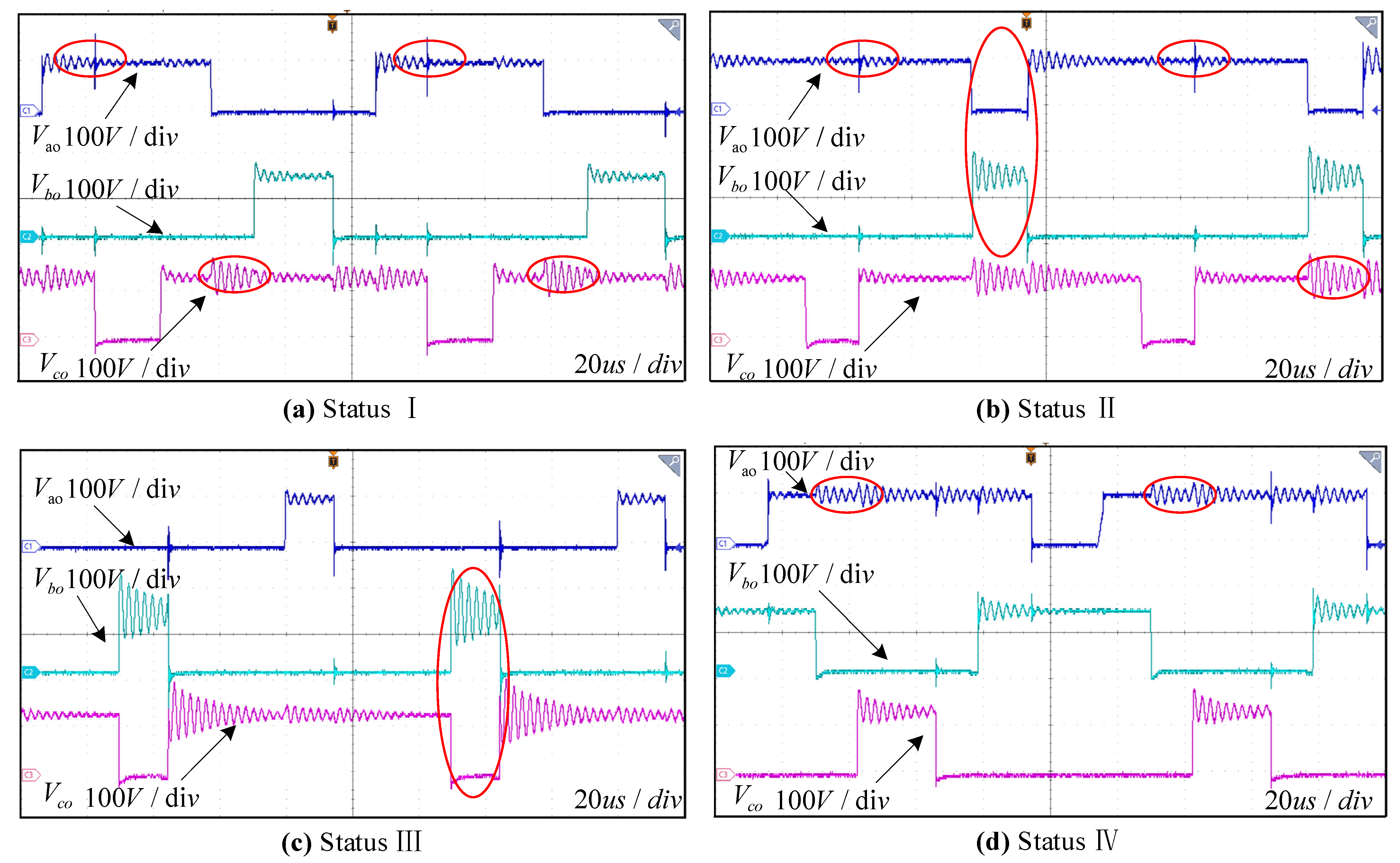
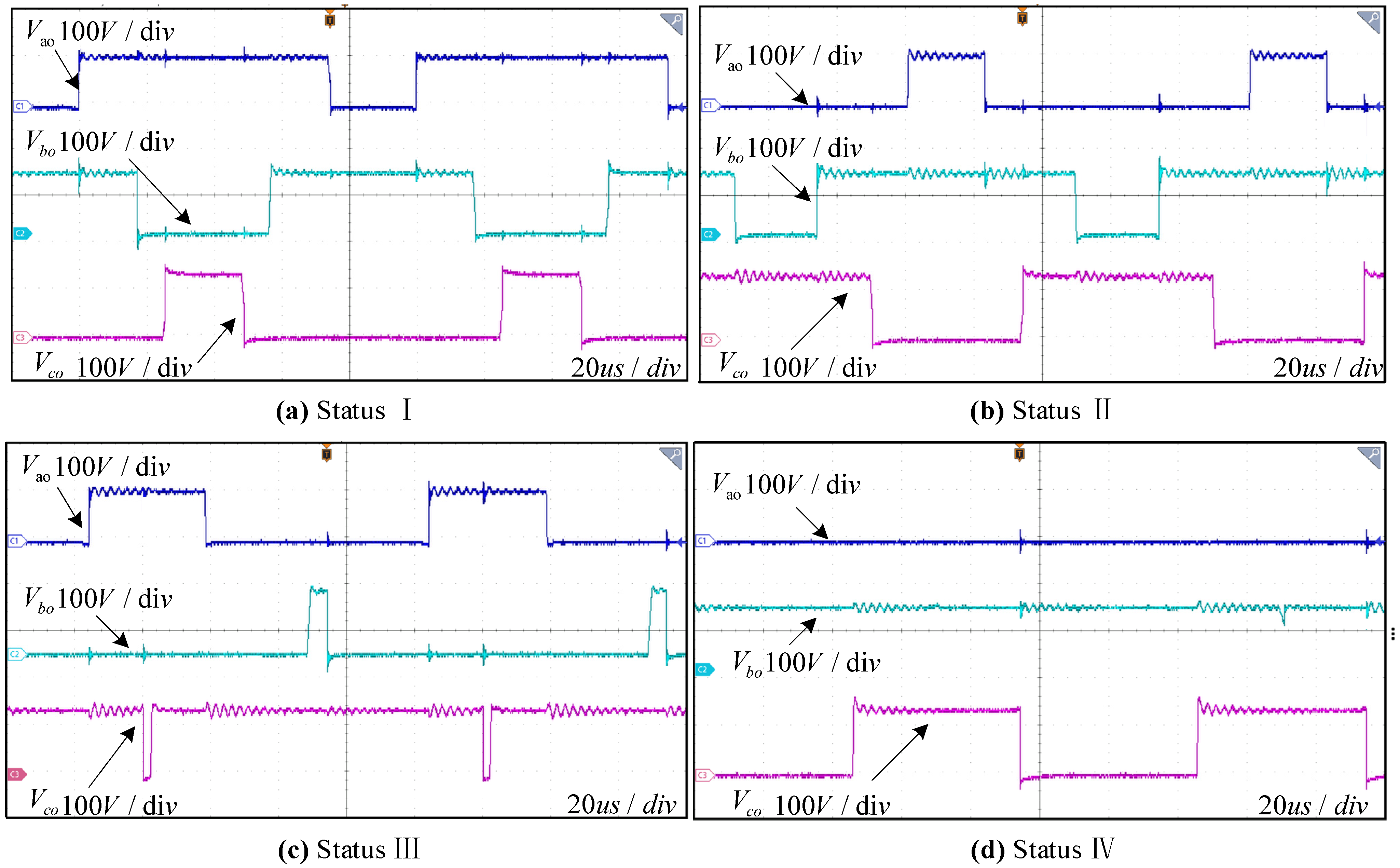
4. Simulation and Experimental Verification

With a switching frequency of 20 kHz, a DC bus voltage of 300 V, and a dead time of 2 us, the simulation results of the motor common-mode voltage generated by SVPWM, AZSPWM and Modified AZSPWM are shown in Figure 7. Under SVPWM, the common-mode voltage generated by the three-phase two-level inverter is a four-step wave that jumps between ± V d c / 2 and ± V d c / 6 , and its frequency hopping rate is 6 times that of the switching frequency. Under AZSPWM, the common-mode voltage waveform is mostly limited to ± V d c / 6 , but there are moments when common-mode suppression fails, resulting in common-mode voltage spikes with an amplitude of ± V d c / 2 . Under Modified AZSPWM, the common-mode voltage waveform is a square wave with an amplitude of ± V d c / 6 , and there exists no common-mode suppression failure moment, which can effectively suppress common-mode voltage spikes.
The experiment platform was a 7.5 KW permanent magnet synchronous motor drag platform, which is driven by Cree CCS050M12CM2 Silicon Carbide full-bridge module. Drive circuit adopted CGD15FB45P1, and the controller was TMS320F28335 control chip produced by TI company. Current sampling adopted Hall Current Sensor HNC-50LT for measurement. The measuring instruments were CYBERTEK DP6150B and Tektronix MDO34 digital oscilloscope, as shown in Figure 8. In order to facilitate the measurement, the common-mode voltage was indirectly measured by measuring the three-phase terminal voltage of the motor. Under SVPWM, AZSPWM, and Modified AZSPWM modulation, the three-phase terminal voltage waveforms of the motor are shown in Figure 9, Figure 10 and Figure 11.
Under SVPWM, there are serious voltage oscillations and over-voltage phenomena at the moment of switching action, which is the most serious at the moment of zero-vector switching. Additionally, traditional AZSPWM can alleviate the high-frequency voltage oscillation in the SiC switching process, but there will be phenomena such as multiple switches operating at the same time, incomplete attenuation of voltage oscillation during the conduction time, and overvoltage. Modified AZSPWM ensures only one switching action at the time of sector conversion, avoiding rapid jumps in line voltage polarity. By selecting different dead-zone compensation strategies, it can effectively suppress high-frequency voltage oscillation and overvoltage phenomena, thereby reducing the common-mode voltage. The amplitude of common-mode voltage is limited to ± V d c / 6 , so that high-frequency common-mode voltage can be effectively suppressed.

5. Conclusions

In this paper, high-frequency common-mode voltage in the SiC motor drive system is analyzed and researched in detail. By analyzing the switching characteristics of SiC devices under different switching states, a no-zero-vector modulation method is selected to suppress the common-mode voltage. The influence of the dead zone effect of traditional no-zero vector modulation under high switching frequency is analyzed, and an improved zero-free vector modulation method is proposed to suppress the high-frequency common-mode voltage of the system.
  • The root of high-frequency common-mode voltage oscillation in SiC motor drive system is from the voltage V d s oscillation during the conduction process of the SiC device. At the time of switching, the higher the amplitude of the common-mode voltage, the stronger the high-frequency voltage oscillation of the SiC device. In the zero vector (000, 111) state, the common-mode voltage amplitude is the highest, and the high-frequency voltage oscillation generated by the device is the most serious.
  • Traditional AZSPWM method for suppressing common-mode voltage causes the problem of simultaneous operation of two-phase switches. At high switching frequencies, the dead zone effect causes common-mode suppression to fail, resulting in common-mode voltage spikes with an amplitude of ± V d c / 2 . The improved AZSPWM adds a set of complementary device turn-on logic to ensure that only one switch acts at the same time, avoiding common-mode voltage spikes caused by sector switching. In view of the influence of the dead zone effect of different switches, different dead zone compensation methods are selected to limit the common-mode voltage amplitude to ± V d c / 6 .
  • Without increasing hardware cost and sacrificing SiC switching speed, the improved AZSPWM proposed in this paper can solve common-mode voltage suppression failure caused by the dead-zone effect at a high switching frequency and suppress high-frequency voltage oscillation and the overvoltage phenomenon. This can effectively suppress high-frequency common-mode voltage, thereby alleviating the negative effects of high-frequency common-mode voltage in SiC motor drive systems.

Author Contributions

Conceptualization, H.L., A.Z. and X.X.; methodology, H.L., A.Z. and X.X.; software, A.Z.; validation, H.L., A.Z. and X.X.; formal analysis, H.L., A.Z. and X.X.; investigation, H.L. and X.X.; resources, H.L. and X.X.; data curation, A.Z.; writing—original draft preparation, A.Z.; writing—review and editing, H.L. and X.X.; visualization, H.L. and X.X.; supervision, H.L. and X.X.; project administration, H.L. and X.X.; funding acquisition, H.L. and X.X. All authors have read and agreed to the published version of the manuscript.

Funding

This research was funded by the Science and Technology Research Program of Chongqing Municipal Education Commission (Grant No. KJQN201900110) and the Fundamental Research Funds for the Central Universities (Grant No.2021CDJJMRH-004).

Conflicts of Interest

The authors declare no conflict of interest.

References

  1. Hamada, K.; Nagao, M.; Ajioka, M.; Kawai, F. SiC—Emerging Power Device Technology for Next-Generation Electrically Powered Environmentally Friendly Vehicles. IEEE Trans. Electron. Devices 2015, 62, 278–285. [Google Scholar] [CrossRef]
  2. Hazra, S.; De, A.; Cheng, L.; Palmour, J.; Schupbach, M.; Hull, B.A.; Allen, S.; Bhattacharya, S. High Switching Performance of 1700-V, 50-A SiC Power MOSFET Over Si IGBT/MOSFET for Advanced Power Conversion Applications. IEEE Trans. Power Electron. 2016, 31, 4742–4754. [Google Scholar]
  3. Willwerth, A.; Roman, M. Electrical bearing damage—A lurking problem in inverter-driven traction motors. In Proceedings of the 2013 IEEE Transportation Electrification Conference and Expo (ITEC), Metro Detroit, MI, USA, 16–19 June 2013; pp. 1–4. [Google Scholar]
  4. Han, D.; Morris, C.T.; Lee, W.; Sarlioglu, B. Comparison Between Output CM Chokes for SiC Drive Operating at 20- and 200-kHz Switching Frequencies. IEEE Trans. Ind. Appl. 2017, 53, 2178–2188. [Google Scholar] [CrossRef]
  5. Hedayati, M.H.; Acharya, A.B.; John, V. Common-Mode Filter Design for PWM Rectifier-Based Motor Drives. IEEE Trans. Power Electron. 2013, 28, 5364–5371. [Google Scholar] [CrossRef]
  6. Gao, Q.; Xu, D. Design of common-mode and differential-mode voltage dv/dt filter at PWM inverter output ter-minals. Trans. China Electrotech. Soc. 2007, 22, 79–84. [Google Scholar]
  7. Jiang, Y.; Chen, X.; Xu, D.; Ma, H. A novel feed-forward-type active filter to eliminate shaft voltage and bearing current at motor terminal in a PWM inverter drives. Proc. CSEE 2003, 49, 25–28. [Google Scholar]
  8. Zhou, J.; Wu, X.; Jiang, Z. A novel 3D-SVPWM algorithm for four-leg converter. Proc. CSEE 2011, 31, 1–8. [Google Scholar]
  9. Hava, A.M.; Ün, E. A High-Performance PWM Algorithm for Common-Mode Voltage Reduction in Three-Phase Volt-age Source Inverters. IEEE Trans. Power Electron. 2011, 26, 1998–2008. [Google Scholar] [CrossRef]
  10. Zhou, J.; Wei, C.; Yang, Y. Simplified PWM algorithm and common mode voltage suppression strategy for three phase inverter. Trans. China Electrotech. Soc. 2014, 29, 158–165. [Google Scholar]
  11. Han, Y.; Lu, H.; Li, Y.; Chai, J. Analysis and Suppression of Shaft Voltage in SiC-Based Inverter for Electric Vehicle Applications. IEEE Trans. Power Electron. 2019, 34, 6276–6285. [Google Scholar] [CrossRef]
  12. Lai, Y.-S.; Bowes, S. A new suboptimal pulse-width modulation technique for per-phase modulation and space vector modulation. IEEE Trans. Energy Convers. 1997, 12, 310–316. [Google Scholar] [CrossRef]
  13. Lai, Y.-S.; Shyu, F.-S. Optimal common-mode Voltage reduction PWM technique for inverter control with con-sideration of the dead-time effects-part I: Basic development. IEEE Trans. Ind. Appl. 2004, 40, 1605–1612. [Google Scholar] [CrossRef]
  14. Lu, H.; Qu, W.; Cheng, X.; Fan, Y.; Zhang, X. A Novel PWM Technique With Two-Phase Modulation. IEEE Trans. Power Electron. 2007, 22, 2403–2409. [Google Scholar] [CrossRef]
  15. Un, E.; Hava, A.M. A Near-State PWM Method With Reduced Switching Losses and Reduced Common-Mode Voltage for Three-Phase Voltage Source Inverters. IEEE Trans. Ind. Appl. 2009, 45, 782–793. [Google Scholar] [CrossRef]
  16. Hava, A.M.; Ün, E. Performance Analysis of Reduced Common-Mode Voltage PWM Methods and Comparison with Standard PWM Methods for Three-Phase Voltage-Source Inverters. IEEE Trans. Power Electron. 2009, 24, 241–252. [Google Scholar] [CrossRef]
Figure 1. Structure diagram of three-phase voltage source inverter.
Wevj 12 00111 g001
Figure 2. Double Pulse Test of SiC Three-phase Full Bridge.
Wevj 12 00111 g002
Figure 3. Double-pulse test results.
Wevj 12 00111 g003
Figure 4. Reduced Common-Mode Voltage PWM.
Wevj 12 00111 g004
Figure 5. Conduction logic sequence of AZSPWM.
Wevj 12 00111 g005
Figure 6. Modified-AZSPWM.
Wevj 12 00111 g006
Figure 7. Common-mode voltage waveform at 20 kHz switching frequency.
Wevj 12 00111 g007
Figure 8. Experimental platform.
Wevj 12 00111 g008
Figure 9. Three-phase voltage waveform of SVPWM different switching states.
Wevj 12 00111 g009
Figure 10. Three-phase voltage waveform of AZSPWM different switching states.
Wevj 12 00111 g010
Figure 11. Three-phase voltage waveform of Modified-AZSPWM different switching states.
Wevj 12 00111 g011
Table 1. Relationship between switching vectors and common-mode voltage.
Vectors V a o V b o V c o V n o
000 V d c / 2 V d c / 2 V d c / 2 V d c / 2
100 V d c / 2 V d c / 2 V d c / 2 V d c / 6
110 V d c / 2 V d c / 2 V d c / 2 V d c / 6
010 V d c / 2 V d c / 2 V d c / 2 V d c / 6
011 V d c / 2 V d c / 2 V d c / 2 V d c / 6
001 V d c / 2 V d c / 2 V d c / 2 V d c / 6
101 V d c / 2 V d c / 2 V d c / 2 V d c / 6
111 V d c / 2 V d c / 2 V d c / 2 V d c / 2
Table 2. Voltage Vector Synthesis Logic and Time under Modified AZSPWM.
SectorLogicConditionCompensation T c m p a T c m p b T c m p c
IType I t 1 < 2 t d I ( T s + X Z ) / 4 t d / 2 ( T s X Z ) / 4 + t d / 2 ( T s X + Z ) / 4 t d / 2
Type I t 2 < 2 t d II ( T s + X Z ) / 4 + t d / 2 ( T s X Z ) / 4 t d / 2 ( T s X + Z ) / 4 + t d / 2
IIType II t 2 < 2 t d I ( T s Y + Z ) / 4 + t d / 2 ( T s Y Z ) / 4 t d / 2 ( T s + Y + Z ) / 4 t d / 2
Type II t 3 < 2 t d II ( T s Y + Z ) / 4 t d / 2 ( T s Y Z ) / 4 + t d / 2 ( T s + Y + Z ) / 4 + t d / 2
IIIType I t 3 < 2 t d I ( T s + Y X ) / 4 t d / 2 ( T s Y + X ) / 4 t d / 2 ( T s + Y + X ) / 4 + t d / 2
Type I t 4 < 2 t d II ( T s + Y X ) / 4 + t d / 2 ( T s Y + X ) / 4 + t d / 2 ( T s + Y + X ) / 4 t d / 2
IVType II t 4 < 2 t d I ( T s + Z X ) / 4 t d / 2 ( T s Z X ) / 4 + t d / 2 ( T s Z + X ) / 4 t d / 2
Type II t 5 < 2 t d II ( T s + Z X ) / 4 + t d / 2 ( T s Z X ) / 4 t d / 2 ( T s Z + X ) / 4 + t d / 2
VType I t 5 < 2 t d I ( T s Y + Z ) / 4 + t d / 2 ( T s + Y + Z ) / 4 t d / 2 ( T s Y Z ) / 4 t d / 2
Type I t 6 < 2 t d II ( T s Y + Z ) / 4 t d / 2 ( T s + Y + Z ) / 4 + t d / 2 ( T s Y Z ) / 4 + t d / 2
VIType II t 6 < 2 t d I ( T s Y + X ) / 4 t d / 2 ( T s + Y X ) / 4 t d / 2 ( T s + Y + X ) / 4 + t d / 2
Type II t 1 < 2 t d II ( T s Y + X ) / 4 + t d / 2 ( T s + Y X ) / 4 + t d / 2 ( T s + Y + X ) / 4 t d / 2
Publisher’s Note: MDPI stays neutral with regard to jurisdictional claims in published maps and institutional affiliations.

