Article

Adaptive Sliding-Mode Controller for a Zeta Converter to Provide High-Frequency Transients in Battery Applications

by
Andrés Tobón
1,
Carlos Andrés Ramos-Paja
2,*,
Martha Lucía Orozco-Gutíerrez
3,
Andrés Julián Saavedra-Montes
2 and
Sergio Ignacio Serna-Garcés
1
1
Departamento de Electrónica y Telecomunicaciones, Instituto Tecnológico Metropolitano, Medellín 050013, Colombia
2
Facultad de Minas, Universidad Nacional de Colombia, Medellín 050041, Colombia
3
Escuela de Ingeniería Eléctrica y Electrónica, Universidad del Valle, Cali 760042, Colombia
*
Author to whom correspondence should be addressed.
Algorithms 2024, 17(7), 319; https://doi.org/10.3390/a17070319
Submission received: 17 June 2024 / Revised: 5 July 2024 / Accepted: 8 July 2024 / Published: 21 July 2024

Abstract

:
Hybrid energy storage systems significantly impact the renewable energy sector due to their role in enhancing grid stability and managing its variability. However, implementing these systems requires advanced control strategies to ensure correct operation. This paper presents an algorithm for designing the power and control stages of a hybrid energy storage system formed by a battery, a supercapacitor, and a bidirectional Zeta converter. The control stage involves an adaptive sliding-mode controller co-designed with the power circuit parameters. The design algorithm ensures battery protection against high-frequency transients that reduce lifespan, and provides compatibility with low-cost microcontrollers. Moreover, the continuous output current of the Zeta converter does not introduce current harmonics to the battery, the microgrid, or the load. The proposed solution is validated through an application example using PSIM electrical simulation software (version 2024.0), demonstrating superior performance in comparison with a classical cascade PI structure.

1. Introduction

Current industrial processes are crucial in pursuing high efficiency, reliability, and adaptability [1,2]. Harnessing the power of data and optimization algorithms is imperative, as they are the key to improving the system’s control, which is needed to stay competitive in the evolving industrial landscape. Artificial intelligence (AI) algorithms and data-driven optimization models for intelligent manufacturing processes have been used to improve production efficiency, reduce costs, and improve the quality of manufacturing services [3,4]. The use of optimization algorithms to obtain profitable, productive, controllable, safe, and sustainable processes is presented in [5,6]. In particular, Ref. [5] reviews multi-objective algorithms for energy production, supply chains, and chemical industries.
Meanwhile, in  Ref. [6], genetic algorithms (GAs) and artificial neural networks (ANNs) are used to define the objective function of the optimization algorithms applied in the metallurgical industry. In addition, Ref. [7] highlights algorithms for data-based industrial process prediction, namely time series and factor-based predictions. That work tests different prediction techniques in multiple steel plant processes.
Energy transition has forced industries to focus on critical processes such as managing electrical energy storage systems (ESSs). Multiple works have focused on ESS characterization, including the description of their components, control strategies, applications, and technologies for high-power systems [8,9,10], as well as their use in multi-source power systems [11], their techno-economic assessment when integrated with renewable energy [12], and the implementation of battery management systems (BMSs) [13]. These systems are fundamental in electrical vehicles (EVs) and microgrids (MGs) based on renewable energy. For example, for EVs under heavy-duty conditions, Ref. [14] evaluates different energy storage system topologies, and Ref. [15] presents a comparison study of semi-active ESS topologies for EVs. Ref. [16] provides a critical review of devices with high energy density and high power density used in electrical transportation; meanwhile, Ref. [17] reports a review of standards and challenges of ESSs for EVs. Moreover, Ref. [18] implements several control schemes tested on EVs with a real driving cycle. Similarly, Ref. [19] presents a systematic review of ESS control techniques for grid-connected and standalone systems based on artificial intelligence. In contrast, Ref. [20] discusses the importance of ESSs in MGs with renewable energy sources.
Among energy storage systems, hybrid ESSs (HESSs) are relevant since the joint operation of complementary energy sources, i.e., sources with high energy density and sources with high power density, guarantees improved power quality, increased energy efficiency, and better dynamic response. Ref. [10] presents examples of HESS installations that improve grid stability and power quality with frequency regulation. A detailed review of HESS benefits is reported in Ref. [20], where the contributions of HESS to MGs are highlighted. For example, HESSs contribute to power quality, offering the MG the ability to provide clean and stable power with a constant power flow, as well as a wave-pure and noise-free sinusoidal within the acceptable frequency and voltage limits. Similarly, Ref. [21] evaluates the capabilities of HESSs to mitigate fluctuations and uncertainty of renewable energy. ESSs with high power density, like supercapacitors or flywheels [21,22], can support loads that demand fast power peaks, while ESSs with high energy density, like batteries [21,23], can provide sustained power for a long time (hours or days).
Different topologies exist for implementing HESSs depending on the converters action; those systems are denominated as passive, semi-active, or fully active. In a passive HESS, any source is managed using a converter, while in semi-active HESS, converters manage some of the sources. For example, the battery pack is regularly connected to the DC bus, while a DC/DC converter manages the supercapacitor [24,25]. Finally, in a fully active HESS, each source is managed by a dedicated converter. Some reviews on topologies for HESS have been published in the last few years. According to the analysis reported in [26], multi-input, multi-port, coupled-inductor, switched-capacitor, and z-source/quasi-z-source converter are suitable for a HESS formed by a battery and a supercapacitor. Those topologies provide bidirectional power flow in EVs, DC MGs, and renewable energy applications. Ref. [16] reports a broad analysis of passive, semi-active, and fully active topologies for HESSs formed by a battery and a supercapacitor. That article highlights the strengths, weaknesses, and opportunities associated with each HESS setup. Ref. [27] also reviews the state of the art on HESS topologies, including reconfigurable topologies at the cell and module levels. Similarly, four semi-active HESSs are discussed in Ref. [15], which are based on supercapacitors and batteries.
Many works on HESSs with semi-active and fully active configurations have been recently published. In Refs. [28,29], a PV system with a fully active HESS, formed by a battery, a supercapacitor (SC), and a bidirectional buck-boost converter, is tested with several algorithms, namely classical PI, an ANN, and Model Predictive Control (MPC). In that work, the mathematical model of the controllers is presented, but the implementation of the algorithms is not discussed. In Ref. [30], the combined control between an optimization algorithm and a neural network is applied to a bidirectional DC-DC converter of an EV; the authors state that algorithms enhanced performance and reduced computation time compared with other methods; however, the implementation is not discussed. In Ref. [31], a fully active HESS formed by a PV array, a battery, and a supercapacitor is presented. The control algorithms for each converter are classical PI structures, and the references for the controllers of both the battery and the supercapacitor converters are based on a power management strategy, in which the missing power on the load is first compensated with the battery and later with the supercapacitor. A structure similar to that reported in [31] is proposed in [25], but there is a fuel cell instead of a PV array. In that work, a fuzzy logic algorithm of 36 rules controls an energy management unit (EMU), which distributes the power among sources and sets the references for the centralized algorithm that controls all HESS converters.
Table 1 summarizes the characteristics of some works published in recent years with HESSs similar to the solution proposed in this manuscript. The review shows that HESSs are based on SCs and batteries, fully active topologies, and buck-boost converters. Control algorithms are diverse, but the classical PI structure is the most common solution. However, some works adopt control schemes based on intelligent algorithms (ANN, Recalling-Enhanced Recurrent Neural Network—RERNN), optimization algorithms (Sand Cat Swarm Optimization—SCSO, MPC), and non-linear algorithms (Supertwisting Sliding Mode Controller—SSMC). Nevertheless, none of the analyzed references implement the HESS with a Zeta converter managing the storage devices; only one reference controls the system with sliding-mode control, but it does not protect the battery from fast current transients.
This manuscript introduces a unique HESS system with a semi-active topology. In this system, the SC is managed by a bidirectional converter, and the battery is directly connected to the DC bus (see Figure 1). The main feature of this setup is the use of a bidirectional Zeta converter and a sliding-mode controller (SMC). The Zeta converter has two key features; it works with any conversion relations and it has a continuous output current. In this way, the Zeta converter can connect any SC with any battery, and it prevents currents with high derivatives in the battery, decreasing its degradation. Furthermore, the SMC has several advantages when used with switching converters. First, its output is a binary signal, which fits perfectly with the converter control input, avoiding the implementation of a Pulse-Width Modulator (PWM); second, the SMC is a non-linear technique that is able to ensure global stability; third, the SMC is robust to variations in the system parameters; and finally, the SMC is integrated into a co-design process of the plant/controller, which is another contribution of this paper. The SMC algorithm proposed in this manuscript ensures three essential conditions:
  • Stable DC/DC converter operation.
  • Reduced harmonics in the battery current.
  • Safe SC voltage regulation.
In summary, the device proposed in this manuscript is a semi-active HESS. Its purpose is to help the battery to deliver fast current transients to the load without altering the power management or the bus control system. Hence, the device’s installation and operation are transparent to the microgrid.
This manuscript is organized into five more sections: Section 2 presents the modeling of the power circuit, where the switched model, average model, stability conditions, and current/voltage ripple are discussed. In addition, Section 3 shows the design and analysis of the SMC, where the switching function is defined, the global stability is demonstrated, the closed-loop dynamic is designed, and the switching frequency limitation is imposed. The design process of the converter and the controller is presented in Section 4, where the algorithms for the selection of passive components and the implementation of the SMC law are illustrated; this section also includes the design of the high-pass filter used to avoid high-frequency current harmonics in the battery. The algorithms for the adaptive SMC’s digital implementation and the PSIM simulations are discussed in Section 5, where the digital implementation reduces the computational burden on a low-cost microcontroller. Finally, the conclusions close the manuscript.
In summary, the contributions of this paper are:
  • Definition of the algorithms for designing the power stage and the adaptive SMC.
  • Providing a battery current without high-frequency transients.
  • Algorithms for implementing the adaptive SMC on low-cost microcontrollers with low computation burden.

2. Power Circuit Modeling

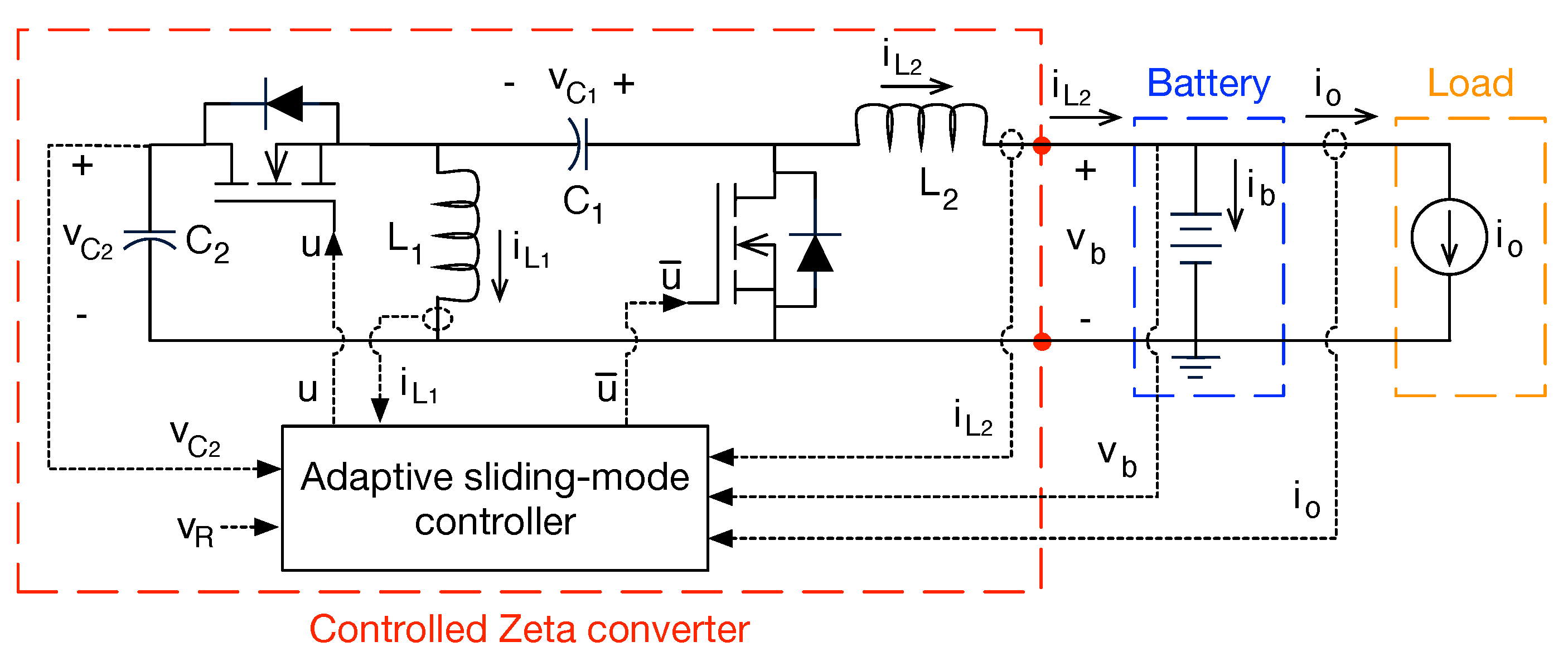
The proposed solution considers the parallel connection of a bidirectional Zeta converter with the battery to be supported; the electrical scheme of this solution is depicted in Figure 2. This circuit describes the electrical structure of the bidirectional Zeta converter, which is formed by two capacitors ( C 1 and C 2 ), two inductors ( L 1 and L 2 ), and two MOSFETs. In addition, the proposed solution requires a fast controller with a wide operation range because the Zeta converter must be stable for capacitor voltages lower, equal to, or higher than the battery voltage; also, it must support positive, negative, and null current conditions. Therefore, the proposed solution includes the design of an adaptive sliding-mode controller (adaptive SMC) to ensure the correct operation of the system. The adaptive SMC requires two voltage sensors, one for the capacitor C 2 voltage ( v C 2 ) and another for the battery voltage ( v b ). It also requires three current sensors, one for the L 1 current ( i L 1 ), another for the L 2 current ( i L 2 ), and a final one for the load/microgrid current ( i o ) that is served by the battery.
The design of the adaptive SMC requires a control-oriented model of the power system. Such a model is obtained by writing the differential equations of the inductor currents and capacitor voltages for each possible state of the control signal, i.e., u = 1 and u = 0 , following the classical method based on charge and volt-second balances reported in [32]. For the first condition ( u = 1 ), the differential equations are given in Equations (1)–(4).
d i L 1 d t = v C 2 L 1
d i L 2 d t = v C 1 + v C 2 v b L 2
d v C 1 d t = i L 2 C 1
d v C 2 d t = i L 1 + i L 2 C 2
Similarly, for the second condition ( u = 0 ), the differential equations are given in Equations (5)–(8).
d i L 1 d t = v C 1 L 1
d i L 2 d t = v b L 2
d v C 1 d t = i L 1 C 1
d v C 2 d t = 0
The previous two sets of equations must be mixed into a single set of non-linear differential equations, thus forming the switched model of the power system given in Equations (9)–(12). In such a model, u is the control signal of the MOSFETs, and u ¯ = 1 u is the complementary control signal.
d i L 1 d t = v C 2 · u v C 1 · u ¯ L 1
d i L 2 d t = v C 1 + v C 2 · u v b L 2
d v C 1 d t = i L 2 · u + i L 1 · u ¯ C 1
d v C 2 d t = i L 1 + i L 2 · u C 2
The switched model can be averaged within the switching period to generate the averaged model, which is useful for analyzing the main dynamic behavior of the power system; this modeling strategy is documented in [32]. Taking into account that the duty cycle d corresponds to the average value of the control signal u, as given in Equation (13), the averaged model of the power system is obtained as reported in Equations (14)–(17), where d = 1 d is the complementary duty cycle and T s w is the switching period.
d = 1 T s w · 0 T s w u d t
d i L 1 d t = v C 2 · d v C 1 · d L 1
d i L 2 d t = v C 1 + v C 2 · d v b L 2
d v C 1 d t = i L 2 · d + i L 1 · d C 1
d v C 2 d t = i L 1 + i L 2 · d C 2
Finally, the steady-state conditions of the power system are obtained from the averaged model by considering the derivatives equal to zero, as described in [32]:
v C 1 = v b
v C 2 = 1 d d · v b
i L 1 = d 1 d · i L 2
Another important analysis concerns the current and voltage ripples in the power system. Then, the magnitude of the ripples on the inductor currents i L 1 and i L 2 is calculated from Equations (5) and (6) following the method reported in [32]:
Δ i L 1 = v b · d · T s w 2 · L 1
Δ i L 2 = v b · d · T s w 2 · L 2
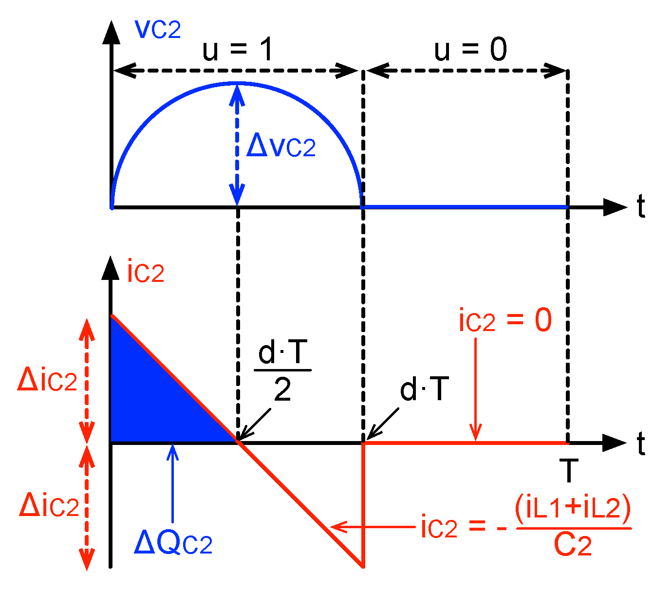
The magnitude of the voltage ripple in the C 2 capacitor must be calculated from the charge stored and extracted from the capacitor during a switching period. Figure 3 shows the C 2 voltage and current ripple waveforms, where current i C 2 is obtained from Equation (12). The charge stored in C 2 when i C 2 is positive is equal to the charge extracted when i C 2 is negative due to the charge balance principle, and it is equal to Δ Q C 2 = d · T s w · Δ i C 2 / 4 . Such a charge is also related to the voltage change in C 2 as Δ Q C 2 = C 2 · Δ v C 2 , where Δ v C 2 is the voltage ripple at C 2 . Moreover, since both i L 1 and i L 2 are in phase, as observed in Equations (1), (2), (5) and (6), the ripple magnitude in the C 2 current is Δ i C 2 = Δ i L 1 + Δ i L 2 . Finally, the magnitude of the voltage ripple in the C 2 capacitor is given as follows:
Δ v C 2 = d · Δ i L 1 + Δ i L 2 · T s w 4 · C 2 = d · d · v b · T s w 2 8 · C 2 · 1 L 1 + 1 L 2
In addition, Figure 3 also shows that the peak value of the current ripple occurs when the voltage ripple is equal to zero; similarly, the peak value of the voltage ripple occurs when the current ripple is equal to zero. This condition will be important in the analysis of the switching frequency reported in Section 3.5.

3. Design and Analysis of the Sliding-Mode Controller

The sliding-mode controller must be designed to ensure the following conditions:
  • Stable operation of the Zeta converter, which requires the stable relation between i L 1 and i L 2 currents given in Equation (20).
  • Regulate the output current of the Zeta converter ( i L 2 ) to provide the high-frequency components of the load current ( i o ), and at the same time, regulate the C 2 voltage to avoid a deep discharge or a dangerous overcharge.
The first condition is ensured by introducing the first part of the switching function Ψ given in Equation (24), which corresponds to relation (20). The second condition is achieved by introducing the second part of Ψ . The i R value is provided by a high-pass filter, which is discussed in Section 4.2 and Section 4.4; the deviation of the C 2 voltage from the safe value v R is also introduced in this second part, where the value of the k v gain will be discussed in Section 3.4. Finally, the sliding surface Φ forces the switching function to slide around zero to impose a null error; this is formalized in Equation (25).
Ψ = k c · i L 2 i L 1 First part + i R + k v · v R v C 2 i L 2 Second part where k c = d d
Φ = Ψ = 0
The feasibility of designing an SMC based on the previous surface must be confirmed using the transversality, reachability, and equivalent control analyses discussed in [33]; the following subsections report the results of those analyses.

3.1. Transversality Analysis

The transversality condition evaluates the controller’s capability to modify the power system’s behavior. Such an evaluation is focused on verifying the presence of the control variable u in the derivative of the switching function, which defines the trajectory of the SMC. The formalization of this test is the following:
d d u d Ψ d t 0
Therefore, the time derivative of the switching function (24) is calculated:
d Ψ d t = k c 1 · v C 1 + v C 2 · u v b L 2 v C 2 · u v C 1 · u ¯ L 1 . . . + d i R d t k v · i L 1 + i L 2 · u C 2
Then, evaluating the transversality value using the previous derivative leads to the following equation:
d d u d Ψ d t = v C 1 + v C 2 · 2 · d 1 1 d · 1 L 2 1 L 1 + k v · i L 1 + i L 2 C 2
Finally, the design of the parameters of both the Zeta converter and SMC must fulfill the transversality condition (26) using Equation (28); this evaluation is presented in Section 4.3.

3.2. Reachability Analysis

The reachability conditions evaluate the capability of the controller to reach the sliding surface. The analysis is the following:
  • Operating under the surface ( Ψ < 0 ) requires a positive switching function derivative d Ψ d t > 0 to reach the surface ( Ψ = 0 ).
  • Operating above the surface ( Ψ > 0 ) requires a negative switching function derivative d Ψ d t < 0 to reach the surface ( Ψ = 0 ).
The previous analyses are formalized with the following inequalities:
lim Ψ 0 d Ψ d t > 0 lim Ψ 0 + d Ψ d t < 0
The evaluation of those general reachability conditions depends on the value of the transversality condition (28); a positive value of Equation (28) indicates a direct relation between the control signal u and derivative d Ψ d t , i.e., a positive change on u produces a positive derivative d Ψ d t > 0 , and a negative change on u produces a negative derivative d Ψ d t < 0 . Instead, a negative value of Equation (28) indicates an inverse relation between u and d Ψ d t , i.e., a positive change on u produces a negative derivative d Ψ d t < 0 , and a negative change on u produces a positive derivative d Ψ d t > 0 .
Then, for a positive transversality value (28), the general reachability conditions (29) become:
lim Ψ 0 d Ψ d t u = 1 > 0 lim Ψ 0 + d Ψ d t u = 0 < 0
Evaluating the previous inequalities with the switching function derivative (27) leads to the stability conditions given in inequalities (31) and (32). Those dynamic limitations on d i R d t must be fulfilled to ensure the reachability of the desired surface in the case of a positive transversality value.
d i R d t > v C 2 · 2 · d 1 1 d · 1 L 2 1 L 1 k v · i L 1 + i L 2 C 2
d i R d t < v b · 2 · d 1 1 d · 1 L 2 1 L 1
Instead, for a negative transversality value (28), the reachability conditions are given in Equation (33). Evaluating those inequalities produces the stability conditions given in (34) and (35).
lim Ψ 0 d Ψ d t u = 0 > 0 lim Ψ 0 + d Ψ d t u = 1 < 0
d i R d t > v b · 2 · d 1 1 d · 1 L 2 1 L 1
d i R d t < v C 2 · 2 · d 1 1 d · 1 L 2 1 L 1 k v · i L 1 + i L 2 C 2
Finally, the reachability conditions impose a dynamic restriction on the positive and negative changes for i R . Thus, the power system and controller must be designed to achieve the required dynamic response with a stable behavior. This analysis is illustrated in Section 4.3 using an application example.

3.3. Equivalent Control

The equivalent control condition evaluates the average value u e q of the control signal u, which must be constrained by the binary values of u, thus 0 , 1 . In the context of power converters, the average value of u is equal to the duty cycle (13); hence, this equivalent control condition evaluates the non-saturation of the duty cycle:
0 < u e q = d < 1
This analysis is performed inside the sliding surface Ψ = 0 d Ψ d t = 0 . Therefore, it ensures that the system remains inside the surface. Replacing the switching function derivative (27) in d Ψ d t = 0 , and switching u by u e q , leads to the following equivalent control value:
u e q = v b · 2 · d 1 1 d · 1 L 2 1 L 1 d i R d t v C 1 + v C 2 · 2 · d 1 1 d · 1 L 2 1 L 1 + k v · i L 1 + i L 2 C 2
Finally, replacing the equivalent value (37) in inequality (36) produces the same dynamic restrictions on i R obtained from the reachability conditions. Therefore, as demonstrated by Sira-Ramirez in [34], fulfilling both the transversality and reachability conditions ensures that the equivalent control condition is also fulfilled; hence, the duty cycle of the converter will not be saturated.

3.4. Closed-Loop Dynamics

The next step in the design of the adaptive SMC is calculating the switching function parameter k v . Such a design is performed considering a stable operation of the SMC (25); thus, Ψ = 0 implies k c · i L 2 = i L 1 and i L 2 = i R + k v · v R v C 2 , where k c = d d . Since the SMC generates the control signal u, the  C 2 voltage can be described using the averaged model given in Equation (17), which results in the following Equation:
d v C 2 d t = k c C 2 · i L 2
Taking into account that i R is the output of a high-pass filter acting on the load current, the load transients always end with i R = 0 . Therefore, the dynamic behavior of the C 2 voltage is described by the following Equation since i L 2 = k v · v R v C 2 for i R = 0 :
d v C 2 d t = k c C 2 · k v · v R v C 2
Transforming the previous expression to the Laplace domain leads to Equation (40), which describes the closed-loop dynamic behavior of the power system. Since the closed-loop exhibits a first-order dynamic, the settling time of C 2 voltage is given by t s , C 2 = 3.9 · τ C L as reported in [35]. Therefore, the  k v parameter is calculated in terms of the desired settling time using Equation (41), which shows two characteristics; k v is an adaptive value with negative sign, which is important information to finish both the transversality and reachability analyses.
v C 2 v R = 1 τ C L · s + 1 where τ C L = C 2 k c · k v
k v = 3.9 · C 2 k c · t s , C 2

3.5. Switching Frequency

The main problem of theoretical SMC is the infinite switching frequency required for the implementation. A classical solution to this problem is to introduce a hysteresis band Δ Ψ , + Δ Ψ around the sliding surface ( Ψ = 0 ) to limit the switching frequency:
Δ Ψ < Ψ < + Δ Ψ
In that way, since the closed-loop operation imposes Ψ = 0 , the hysteresis band produces the switching function ripple reported in Equation (43). The ripple magnitudes Δ i L 1 and Δ i L 2 were reported in Equations (21) and (22), respectively, and the ripple magnitude Δ v C 2 was reported in Equation (23). Finally, the SMC ensures that i L 2 follows the reference i R provided by the high-pass filter. Hence, the subtraction between those two signals is i R i L 2 = Δ i L 2 .
Δ Ψ = k c · Δ i L 2 Δ i L 1 + Δ i L 2 + k v · Δ v C 2
In steady-state operation, k c · i L 2 = i L 1 , as given in Equation (20), where k c = d d ; thus, i L 2 = i R + k v · v R v C 2 . Therefore, the term k c · Δ i L 2 Δ i L 1 of Equation (43) is equal to zero. Moreover, the analysis reported in Figure 3 shows that the peak value of i L 2 occurs when the ripple in v C 2 is equal to zero; similarly, the peak value of v C 2 occurs when the ripple in i L 2 is equal to zero. Therefore, the peak value of the term Δ i L 2 + k v · Δ v C 2 of Equation (43) occurs at the peak value of i L 2 or at the peak value of k v · Δ v C 2 , depending on which component has the highest magnitude. This condition is formalized with the following equation for the ripple magnitude of the switching function:
Δ Ψ = max Δ i L 2 , k v · Δ v C 2
Finally, Equation (44) is used to design the hysteresis band Δ Ψ , + Δ Ψ in agreement with the maximum switching frequency F s w supported by the MOSFETs used to construct the Zeta converter.

4. Design Procedure and Application Example

This section illustrates the design of both the power stage and the SMC to ensure the desired operation of the battery-supporting system. The first characteristic concerns the battery voltage, which is selected as 48 V due to the wide use of such a voltage level in DC loads and microgrids. The second characteristic is the C 2 nominal voltage, which is selected as 48 V to require a nominal duty cycle near 50%; however, any other value can be selected. Concerning the load transients, this example considers fast current changes up to 70 A/ms with magnitudes of 2 A, where the battery will be protected for frequencies higher than 500 Hz; again, any other values can be used depending on the load and battery characteristics. In addition, the maximum deviation of the C 2 voltage must be limited to 3 % for 100 ms, thus avoiding a large discharge or overcharge of the capacitor. Finally, the maximum switching frequency is selected as 120 kHz, which is a conservative value for commercial applications. Table 2 summarizes the previous characteristics.

4.1. Inductor Design

Taking into account that i L 2 (output current of the Zeta converter) provides the high-frequency components of the load current i o , the maximum derivative of i L 2 must be enough to supply the maximum derivative of i o :
max d i L 2 d t > max d i o d t
Replacing the derivative magnitude of i L 2 given in (6) into (45) leads to the following limit for L 2 :
L 2 < v b max d i o d t
Using the values given in Table 2 in inequality (46) produces L 2 < 685.71 μ H. However, with such a limit value, the MOSFETs will not switch states during the load transient; hence, to improve the dynamic behavior of the converter, L 2 is selected as half of the limit value, which enables the MOSFETs to produce at least two commutations during a current transient. Then, adjusting to a commercial value, L 2 = 330 μ H. Finally, L 1 is set equal to L 2 to balance the current ripple injected into the C 1 capacitor; hence, L 1 = 330 μ H.

4.2. Capacitors and High-Pass Filter Design

The reference current i R in the switching function (24) is generated by a high-pass filter G h p processing the load current i o . Equation (47) describes the first-order high-pass filter considered in this solution.
i R = G h p · i o where G h p = s s + 2 · π · F s a f e
The most extreme transient corresponds to a step current i o = Δ i o s , which produces the following time-domain waveform obtained from the inverse Laplace transformation of Equation (47):
i R = Δ i o · e 2 · π · F s a f e · t
The charge extracted from C 2 during a positive load transient (increment in i o ) is obtained by integrating the previous time-domain waveform:
Q C 2 = 0 Δ i o · e 2 · π · F s a f e · t d t = Δ i o 2 · π · F s a f e
During a positive load transient, the v C 2 voltage is decreased and the voltage deviation is negative, which produces the following charge extraction from C 2 :
Q C 2 = C 2 · v R · M O C 2
Finally, C 2 capacitance is obtained by relating Equations (49) and (50), as follows:
C 2 = Δ i o 2 · π · F s a f e · v R · M O C 2
The design of C 1 is performed to provide a balance with the energy stored in C 2 , which is equal to E C 2 = C 2 · v R 2 / 2 . Taking into account that the energy stored in C 1 is E C 1 = C 1 · v C 1 2 / 2 , the condition for C 1 to achieve E C 1 = E C 2 is calculated using Equations (18) and (19), as follows:
C 1 = C 2 · v R v b 2
Evaluating Equation (51) with the values given in Table 2 produces a capacitance equal to 442.1 μ F, which, adjusted to a commercial value, results in C 2 = 470 μ F. Similarly, evaluating Equation (52) produces the commercial value C 1 = 470 μ F.

4.3. Verification of the SMC Stability

The next step is to evaluate the SMC’s stability, which requires verifying the transversality and reachability conditions. Evaluating the transversality value given in Equation (28) using the characteristics of Table 2 and the parameters previously calculated produces the average value d d u d Ψ d t = 2.9 × 10 5 0 , which confirms the transversality condition (26).
Taking into account that the transversality value is negative, the reachability conditions that must be evaluated are inequalities (34) and (35). Evaluating those inequalities with the characteristics of Table 2 and the parameters previously calculated leads to the restrictions 145 A / ms < d i R d t < 145 A / ms . Since the reference signal i R is generated by a high-pass filter processing the load current i o , as discussed in Section 4.2, the maximum derivative of i R is the same as that of i o : max d i R d t = max d i o d t = 70 A/ms. Therefore, the previous calculations confirm that the reachability conditions (33) are fulfilled. It must be noted that, in case of a positive transversality value, inequalities (31) and (32) must be evaluated.
In conclusion, the proposed design of both the power stage and SMC ensures a stable operation of the system, which guarantees the desired support for the battery.

4.4. SMC Control Law

Since the transversality value is negative, the reachability conditions are defined in (33), which also defines the control law. The reachability condition lim Ψ 0 d Ψ d t u = 0 > 0 requires that u = 0 when Ψ < 0 , and the reachability condition lim Ψ 0 + d Ψ d t u = 1 < 0 requires that u = 1 when Ψ > 0 . However, the hysteresis band Δ Ψ , + Δ Ψ introduced in Section 3.5 modifies the limits of Ψ to produce changes on u, which defines the final control law, as follows:
u = if Ψ Δ Ψ u = 0 u ¯ = 1 if Ψ + Δ Ψ u = 1 u ¯ = 0
Evaluating Equation (44) using the characteristics of Table 2, and the parameters previously calculated, leads to Δ Ψ = 0.3 A.

4.5. Summary of the Design and Control Processes

The summary of the design process for the parameters of both the power stage and SMC is synthesized in Algorithm 1. Such a process starts with the design of inductor L 2 to fulfill the maximum load current derivative. To ensure at least two switching periods within the transient, a constant k L 1 / 2 is used to fulfill inequality (46), where smaller k L produces higher number of periods per transient, but very small L 2 values will require very small Δ Ψ limits, which could introduce implementation problems due to circuit sensitivity. Therefore, k L must be selected to ensure that Δ Ψ magnitude enables the correct operation of the comparators used to implement the control law (53). Next, L 1 is set equal to L 1 to provide a balance in the current ripple of both inductors.
The capacitor C 2 is designed to limit the voltage deviation up to M O C 2 , and  C 1 is designed to balance the energy stored in both capacitors. Then, the steady-state values of both the current ( k c , s s ) and voltage ( k v , s s ) constants are calculated from the nominal values of the application, and both constants are used to calculate the hysteresis band value Δ Ψ . Finally, depending on the application, the high-pass filter is parameterized in agreement with the safe frequency range defined for the battery transients.
Algorithm 1 Design of both the power stage and SMC parameters
Require:  v b , v R , M O C 2 , t s , C 2 , max d i o d t , Δ i o , F s a f e , F s w
  1:
L 2 near commercial value of k L · v b max d i o d t where k L 1 2
  2:
L 1 L 2
  3:
C 2 near commercial value of Δ i o 2 · π · F s a f e · v R · M O C 2
  4:
C 1 near commercial value of C 2 · v R v b 2
  5:
k c , s s v b v R
  6:
k v , s s 3.9 · C 2 k c , s s · t s , C 2
  7:
Δ Ψ max Δ i L 2 , k v , s s · Δ v C 2 calculating Δ i L 2 from (22) and Δ v C 2 from (23)
  8:
G h p s s + 2 · π · F s a f e
  9:
return  L 1 , L 2 , C 1 , C 2 , Δ Ψ , G h p
Implementing the adaptive controller requires processing, in an infinite loop, a series of calculations based on measurements and fixed parameters. Such a control process is synthesized in Algorithm 2. The algorithm requires the desired reference for the voltage in C 2 and the value of the two inductor currents, both the battery and C 2 voltages, and the load current. The next step is to detect the high-frequency transients on the load current using the high-pass filter. Then, both the current ( k c ) and voltage ( k v ) gains are adapted for the actual operation condition, and with those values, the switching function Ψ for the operation conditions is calculated.
Algorithm 2 Control process
Require:  v R
  1:
loop
  2:
     measure  i o , v C 2 , v b , i L 1 , i L 2
  3:
      i R G h p · i o
▹ Filter the load current to detect the fast transients
  4:
      k c v b v C 2
▹ Calculate the adaptive current gain
  5:
      k v 3.9 · C 2 k c · t s , C 2
▹ Calculate the adaptive voltage gain
  6:
      Ψ i R + k v · v R v C 2 + k c 1 · i L 2 i L 1
▹ Calculate Ψ
  7:
     if  Ψ Δ Ψ  then
▹ Apply the control law
  8:
           u 0
  9:
           u ¯ 1
10:
     else if  Ψ + Δ Ψ  then
11:
           u 1
12:
           u ¯ 0
13:
     else
14:
          u u ¯ do not change
15:
     end if
16:
     return u, u ¯
u and u ¯ are provided to the MOSFETs
17:
end loop
Using the values of Ψ and Δ Ψ , the control law of the SMC (53) is executed, which produces the binary values for controlling the MOSFETs (u and u ¯ ). Finally, the loop starts again by measuring the physical variables.
Table 3 summarizes the circuital parameters calculated for this application example. This table also presents the energy stored in the elements of the Zeta converter needed to support the high-frequency transients of the load current. The table shows that the energy stored in the capacitors C 1 and C 2 is very small. In the case of L 2 , since i L 2 is defined by the high-pass filter given in (47), the steady-state value of i L 2 is 0 A, and from Equation (20), it is obtained that the steady-state value of i L 1 is also 0 A; thus, the inductors do not store energy in the steady state, and they operate only as energy buffers during the transient conditions. Therefore, the total energy stored in the Zeta converter is 0.30 mWh or 0.006 mAh.
It must be highlighted that the design of the proposed supporting device (formed by both the Zeta converter and SMC) does not depend on the battery capacity; instead, it only depends on the load transients that must be supported. The battery capacity is related to the load or microgrid operation cycle, which has a low-frequency profile. In contrast, the supporting device capacity only depends on the system’s high-frequency transients.

5. Implementation of the Adaptive SMC and Detailed Circuital Simulations

The power system described in Figure 2 was implemented in the power electronics simulator PSIM using the electrical parameters calculated in the previous section. The adaptive sliding-mode controller can be implemented following Algorithm 2 with analog or digital circuits. The following subsections discuss both implementations.

5.1. Analog Implementation of the Adaptive SMC

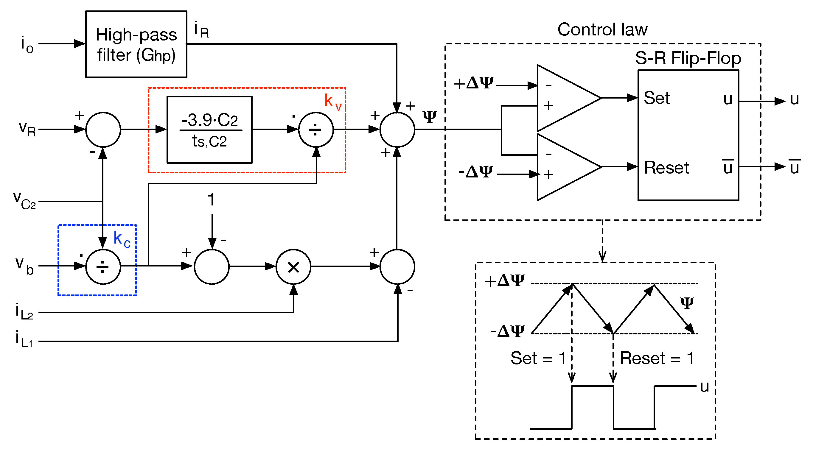
The implementation of the control algorithm, using analog circuits, is presented in Figure 4. Such a circuit considers the implementation of the high-pass filter using operational amplifiers, as discussed in [36]. Similarly, addition, subtraction, and multiplication by a constant value can be easily implemented with operational amplifiers, as reported in [36]. The multiplication and division operations can be implemented using analog integrated circuits like the AD734 described in [37]. Therefore, the calculation of the adaptive parameters k c and k v , the calculation of the i R signal, and the calculation of the switching function Ψ are easily implemented with analog circuits.
Concerning the control law, the logical operations in Algorithm 2 can be implemented using two comparators and an S-R Flip-Flop, as depicted in Figure 4. When Ψ + Δ Ψ , the signal S e t = 1 activates the S e t input of the Flip-Flop, which imposes u = 1 and u ¯ = 0 ; similarly, when Ψ Δ Ψ , the signal R e s e t = 1 activates the R e s e t input of the Flip-Flop, which imposes u = 0 and u ¯ = 1 . Finally, Figure 4 shows a diagram of those control signals.
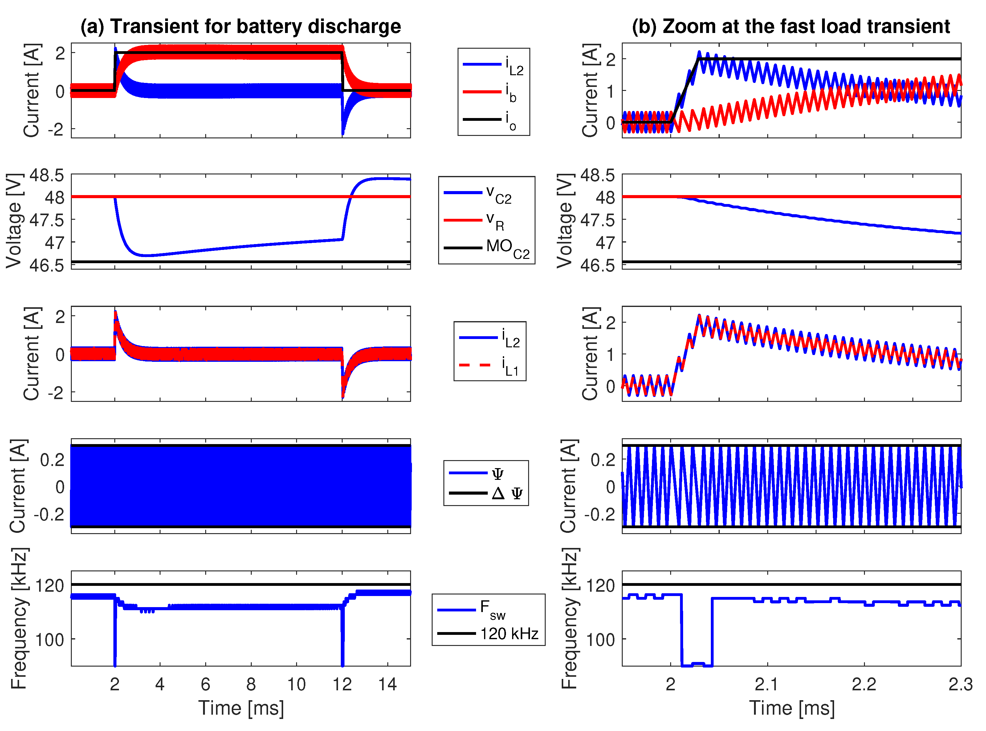
The first simulation of this analog implementation, reported in Figure 5, evaluates the compensation of a load transient from steady state to battery charge with the maximum current derivative d i o d t = 70 A/ms. Figure 5a shows two fast current transients between 0 A and 2 A, and in both cases, the Zeta converter provides the fast current component, while the battery exhibits a slow change in the current, thus fulfilling the desired behavior of the system. In addition, the  C 2 voltage is constrained to the M O C 2 limit for such a transient condition, which validates the design of the converter components. Moreover, since v b = v R , then the average value of k c is near 1 and the stability condition of the inductor currents is i L 1 = i L 2 , which is confirmed in the simulation. It is observed that the switching function Ψ is permanently trapped inside the hysteresis band Δ Ψ , + Δ Ψ ; thus, the SMC is always inside the sliding mode, which ensures the global stability. Finally, the switching frequency is always below the maximum design limit of 120 kHz.
Figure 5b presents a zoom of the previous simulation, which confirms that the Zeta converter provides the current transient, while the battery current changes with the frequency limit defined by the high-pass filter. In addition, the zoom of the inductor currents confirms the relation imposed by the first part of the switching function and confirms both currents’ stable behavior. Finally, the zoom of the switching function Ψ shows the frequency reduction at the perturbation instant, which is caused by the fast change in the load current, where the SMC can impose three switching periods during the transient time.
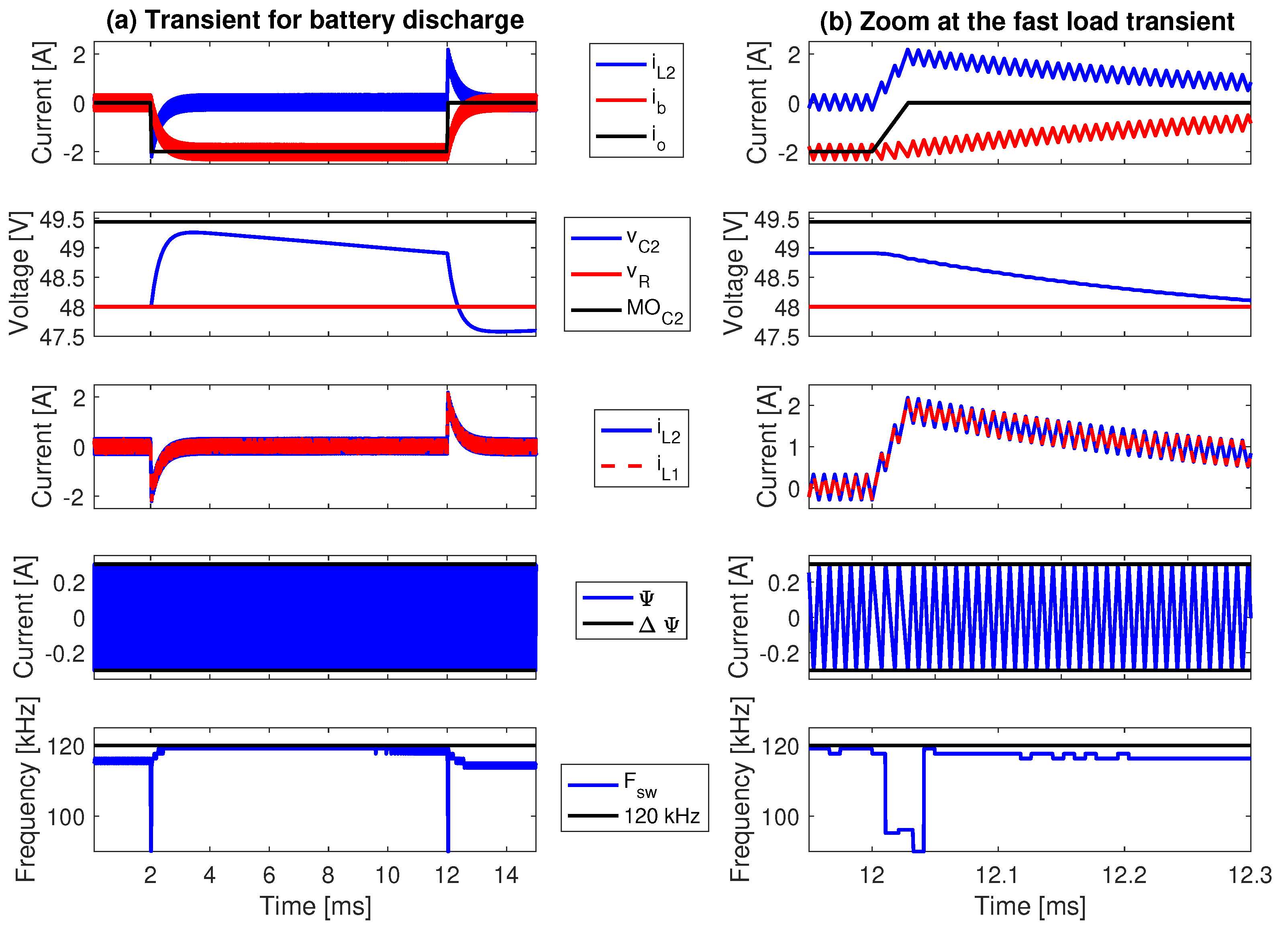
Figure 6 reports a second simulation, which evaluates the compensation of a load transient from steady state to battery discharge with the same maximum current derivative. Figure 6a shows the correct behavior of both the Zeta converter and battery currents, while C 2 voltage and the inductor currents are regulated as expected. As in the previous case, the switching function is constrained to the hysteresis band, ensuring global stability. In this case, Figure 6b shows a zoom for the second transient (from 2 A to 0 A), where the steady-state values of the Zeta current and the battery current are different. After the transient is finished, the Zeta current becomes zero since the supporting device is designed only to provide fast current transients. Therefore, the Zeta converter provides the step-up fast transient from 0 A to 2 A needed to reach the final current of both the battery and the load ( 0 A). As in the previous case, the waveforms of Figure 6b confirm the stability of the proposed solution and the correct limitation of the switching frequency.
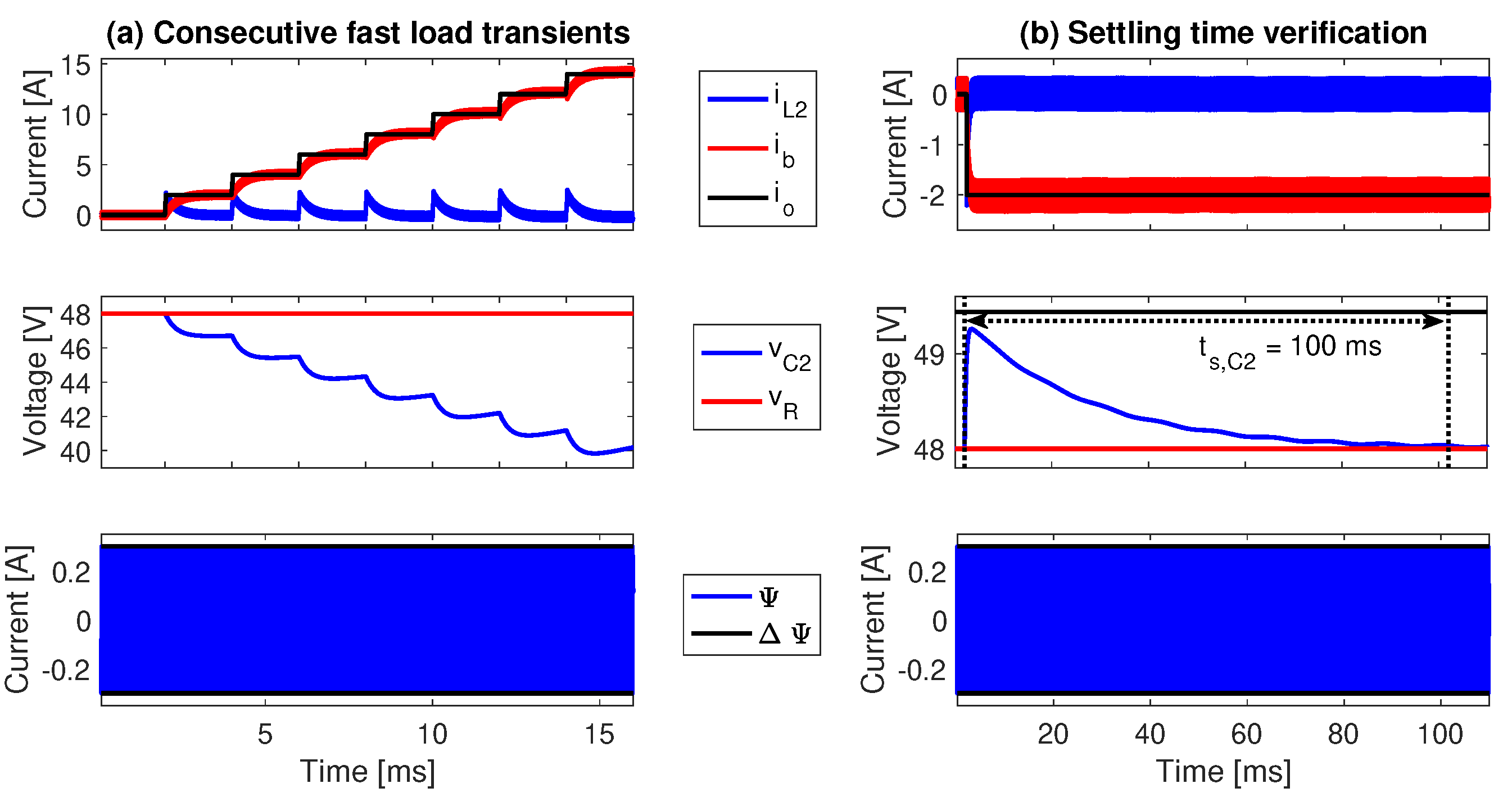
The next simulation, reported in Figure 7a, evaluates the performance of the proposed solution to a sequence of load transients. In this case, the load current changes from 0 A to 14 A with transients of 2 A. As expected, the Zeta converter provides the fast current transients, returning to 0 A for the steady-state condition. Therefore, despite the consistent increment in the battery current, the supporting device (Zeta converter) always provides the same behavior, which prevents the battery from suffering the fast current transients imposed by the load. Since the consecutive transients occur in intervals of 2 ms, which is much shorter than the settling time ( t s , C 2 = 100 ms), the voltage of C 2 capacitor is reduced up to 40 V, but the SMC always operates inside the sliding surface, thus ensuring global stability and demonstrating the adaptability and robustness to changes on the operation conditions.
Figure 7b presents the fourth simulation, which evaluates the settling time of the C 2 voltage. In this test, a single load current perturbation is applied to charge the battery with a load current equal to 2 A. The simulation confirms that C 2 voltage is below the designed deviation M O C 2 for that perturbation, and the voltage compensation is achieved in the designed settling time ( 100 ms). Therefore, both discharging (positive load transients) and charging (negative load transients) times are predictable and equal to the designed settling time. This satisfactory performance confirms that the switching function operates as expected, thus ensuring the capability of providing or absorbing load current transients to protect the battery.

5.2. Digital Implementation of the Adaptive SMC

The proposed SMC can be implemented in a digital microprocessor by coding Algorithm 2 in any supported language. However, such an approach will impose high requirements on the Analog-to-Digital Converters (ADCs) needed to measure the two inductor currents, both the battery and C 2 voltages, and the load current. Since Algorithm 2 produces the control signals u and u ¯ , the time resolution for the rising and falling of u (and u ¯ ) impacts the accuracy of the SMC implementation. Therefore, adopting an acquisition time between 80 and 100 times smaller than the switching period is common, thus providing a resolution for the control signal between 1% and 1.25% of the period. Using such a traditional approach, the implementation of Algorithm 2, for the application characteristics reported in Table 2, will require ADCs with sampling frequencies between 9.6 MSPS ( 9.6 × 10 6 samples per second) and 12 MSPS, which are very high.
Therefore, this section proposes a modified formulation of the practical sliding surface (42) to reduce the ADC sampling frequency. This new formulation represents the high-frequency signal i L 1 of Ψ (24) as a function of the other terms, which results in the following representation of the practical sliding surface Δ Ψ < Ψ < + Δ Ψ :
Ψ L 1 , S e t < i L 1 < Ψ L 1 , R e s e t
Ψ L 1 , R e s e t = i R + k v · v R v C 2 + k c 1 · i L 2 + Δ Ψ
Ψ L 1 , S e t = i R + k v · v R v C 2 + k c 1 · i L 2 Δ Ψ
Then, using the new Ψ formulation given in (54)–(56), we also obtain a new formulation for the control law (53), as follows:
u = if i L 1 Ψ L 1 , R e s e t u = 0 u ¯ = 1 if i L 1 Ψ L 1 , S e t u = 1 u ¯ = 0
Then, two processes are needed. The first one calculates the limits Ψ L 1 , S e t and Ψ L 1 , R e s e t , and the second one uses those limits to calculate the MOSFET signals with Equation (57). Considering that the calculation of Ψ L 1 , S e t and Ψ L 1 , R e s e t requires the measurement of multiple analog signals, this process imposes the requirements in the ADC frequency. Instead, the calculations of u and u ¯ only require simple comparisons; hence, this section proposes using a microcontroller able to perform both processes. For example, the F28379D Microcontroller reported in [38] has multiple ADC channels, has Digital-to-Analog Converters (DACs), and has a Comparator Subsystem (CMPSS). The CMPSS is based on two analog comparators, which have the negative inputs of the comparators connected to two DAC channels, and the positive inputs of the comparators are connected to a single pin of the F28379D. Therefore, two threads can be designed to run with different sampling periods inside the microcontroller, using the CMPSS to perform the analog comparisons of the new control law given in (57).
The first thread (Thread 1) calculates the comparator inputs Ψ L 1 , S e t and Ψ L 1 , R e s e t . Since such a comparison is used in each switching period, the values of Ψ L 1 , S e t and Ψ L 1 , R e s e t must be updated at least twice in each period; thus, the sampling frequency must be at minimum double the maximum switching frequency. From Table 2, it is observed that the application example imposes a maximum switching frequency of 120 kHz, and introducing a safety factor of 10%, the sampling frequency needed is 264 kSPS (0.264 MSPS), hence reducing the sampling frequency to 2.2% of the requirement imposed by the traditional digital implementation. Figure 8 illustrates the digital implementation of the control algorithm, where Thread 1 delivers the limits Ψ L 1 , S e t and Ψ L 1 , R e s e t to the CMPSS.
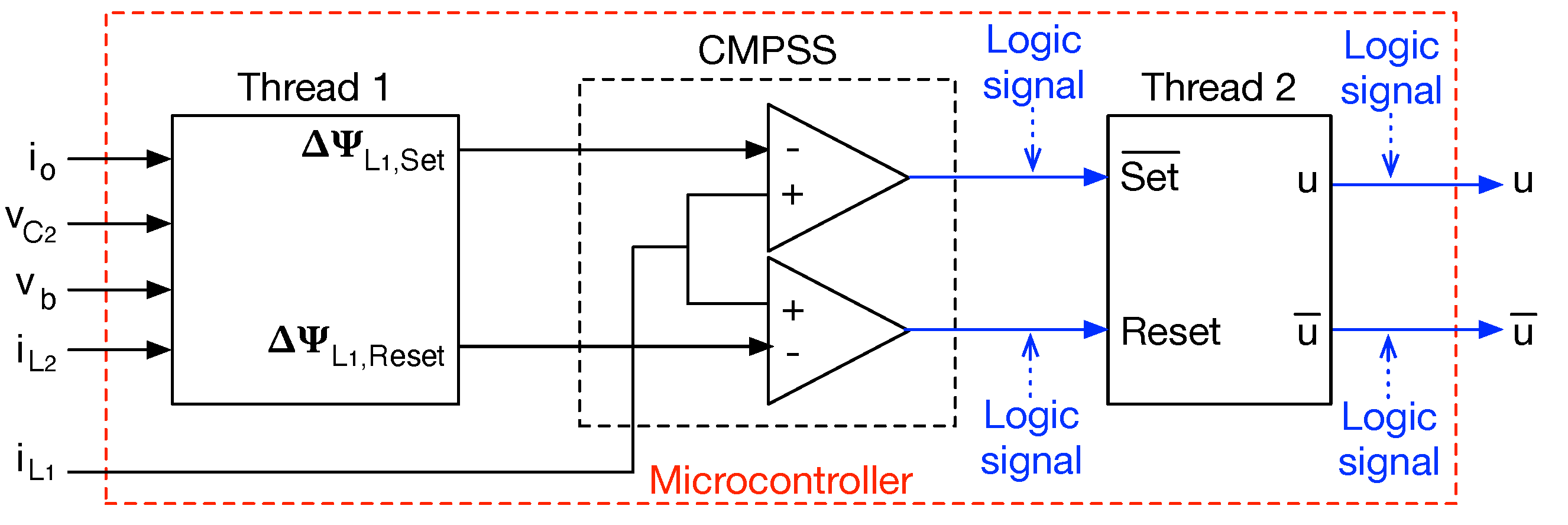
Figure 8 shows that i L 1 is introduced in the CMPSS; hence, an ADC channel is not needed for i L 1 . Since the external input of the CMPSS ( i L 1 ) is connected to the positive inputs of the comparators, the lower comparator correctly produces the reset signal ( R e s e t ). In contrast, the upper comparator produces an inverted version of the set signal ( S e t ¯ = 1 S e t ). The outputs of the CMPSS are logic signals, which is the main advantage of the structure given in Figure 8, since those logic signals can be captured by the second thread (Thread 2) at the full speed of the microprocessor (200 MHz); hence, the capture frequency is not limited by the conversion time of the ADC. Similarly, the control signal of the MOSFETs (u and u ¯ ) are logic signals; therefore, executing Thread 2 at 10 MHz or 12 MHz will provide a resolution between 1% and 1.25% of the switching period for both the rising and falling times of u (and u ¯ ). In fact, executing Thread 2 at the full speed of the F28379D Microprocessor (200 MHz) could improve the resolution of u (and u ¯ ) to 0.06% of the switching period.
Algorithm 3 reports the pseudocode for Thread 1, which calculates the comparator inputs Ψ L 1 , S e t and Ψ L 1 , R e s e t . This algorithm considers the discrete implementation of the high-pass filter given in Equation (58), which is obtained from the analog high-pass filter previously reported in Equation (47) by performing the Tustin transformation s = [ 2 / T a d q ] · [ z 1 ] / [ z + 1 ] discussed in [39], and subsequently applying the inverse Z-transformation to obtain the difference equation representation of i R ( k ) . In such an expression, T a d q is the ADC sampling time. Therefore, Thread 1 can be executed at 264 kHz for the application example, which ensures an ADC frequency of 264 kSPS ( T a d q = 3.8 μ s). The calculations of Ψ L 1 , S e t and Ψ L 1 , R e s e t show that those values are continuous; hence, those signals must be provided to the CMPSS using two DAC channels. The F28379D Microcontroller has DAC channels with minimum conversion times equal to 2 μ s; hence, T a d q = 3.8 μ s can be fulfilled by the on-board DAC. Finally, the values of i R and i o are stored for the next iteration of the algorithm.
i R ( k ) = i o ( k ) i o ( k 1 ) π · F s a f e · T a d q 1 · i R ( k 1 ) π · F s a f e · T a d q + 1
Algorithm 3 Thread 1: calculation of the comparator inputs ( Ψ L 1 , S e t and Ψ L 1 , R e s e t )
Require:  v R , F s a f e , Δ Ψ , T a d q
  1:
loop
  2:
     measure  i o ( k ) , v C 2 ( k ) , v b ( k ) , i L 2 ( k )
  3:
      i R ( k ) i o ( k ) i o ( k 1 ) π · F s a f e · T a d q 1 · i R ( k 1 ) π · F s a f e · T a d q + 1
▹ High-Pass filter
  4:
      k c ( k ) v b ( k ) v C 2 ( k )
▹ Calculate the adaptive current gain
  5:
      k v ( k ) 3.9 · C 2 k c ( k ) · t s , C 2
▹ Calculate the adaptive voltage gain
  6:
      Ψ L 1 , R e s e t ( k ) i R ( k ) + k v ( k ) · v R v C 2 ( k ) + k c ( k ) 1 · i L 2 ( k ) + Δ Ψ
  7:
      Ψ L 1 , S e t ( k ) i R ( k ) + k v ( k ) · v R v C 2 ( k ) + k c ( k ) 1 · i L 2 ( k ) Δ Ψ
  8:
      i R ( k 1 ) i R ( k )
▹ Store i R ( k ) value
  9:
      i o ( k 1 ) i o ( k )
▹ Store i o ( k ) value
10:
     return  Ψ L 1 , S e t ( k ) , Ψ L 1 , R e s e t ( k )
▹ Signals for the comparators of the CMPSS
11:
end loop
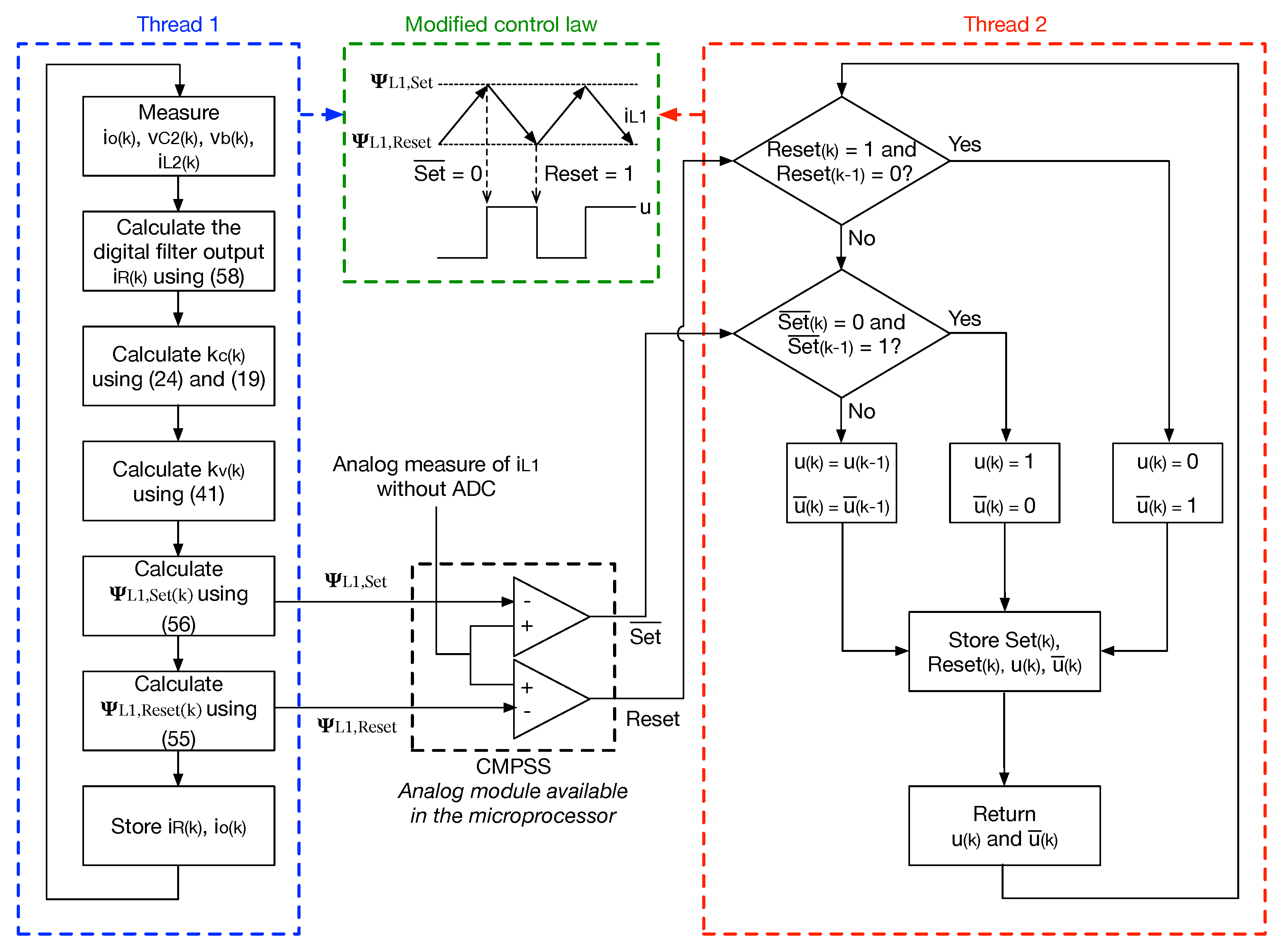
Algorithm 4 reports the pseudocode for Thread 2, which produces the control signals for the MOSFETs (u and u ¯ ); hence, it must be executed between 80 and 100 times the maximum switching frequency. For the application example, 10 MHz was selected. Thread 2 starts by capturing the output signals of the CMPSS ( R e s e t and S e t ¯ ); then, Thread 2 detects if a rising edge on the R e s e t signal has been produced by the CMPSS. To take into account that the set S e t signal produced by the CMPSS is inverted ( S e t ¯ = 1 S e t ), Thread 2 detects if a falling edge on the S e t ¯ signal has been produced. Then, the algorithm changes the MOSFET signals u and u ¯ following the new formulation of the control law previously obtained in Equation (57); if no rising edge on R e s e t or falling edge on S e t ¯ occurs, then u and u ¯ are not changed. The last steps of the algorithm store the states of R e s e t , S e t ¯ , u, and u ¯ for the next iteration. Figure 9 summarizes the digital implementation, where the processes of both threads are synthesized. In addition, the connection of both threads with the analog CMPSS module is illustrated, which occurs inside the microprocessor to generate the MOSFET control signals. Finally, the figure also illustrates the signal processing of the modified control law adopted for this digital implementation.
Algorithm 4 Thread 2: control signal generator (u and u ¯ )
  1:
loop
  2:
      Logic inputs  S e t ¯ ( k ) , R e s e t ( k )
  3:
      if  R e s e t ( k ) = 1 & R e s e t ( k 1 ) = 0  then
▹ Detect rising edge in R e s e t
  4:
            u ( k ) 0
  5:
            u ¯ ( k ) 1
  6:
      else if  S e t ¯ ( k ) = 0 & S e t ¯ ( k 1 ) = 1  then
▹ Detect falling edge in S e t ¯
  7:
            u ( k ) 1
  8:
            u ¯ ( k ) 0
  9:
      else
10:
            u ( k ) u ( k 1 )
u ( k ) does not change
11:
            u ¯ ( k ) u ¯ ( k 1 )
u ¯ ( k ) does not change
12:
      end if
13:
       S e t ¯ ( k 1 ) S e t ¯ ( k )
▹ Store S e t ¯ ( k ) value
14:
       R e s e t ( k 1 ) R e s e t ( k )
▹ Store R e s e t ( k ) value
15:
       u ( k ) u ( k 1 )
▹ Store u ( k ) value
16:
       u ¯ ( k ) u ¯ ( k 1 )
▹ Store u ¯ ( k ) value
17:
      return  u ( k ) , u ¯ ( k )
u ( k ) and u ¯ ( k ) are provided to the MOSFETs
18:
end loop
The digital implementation of the SMC reported in Figure 9 was performed in the power electronics simulator PSIM, as follows. Thread 1 and Thread 2 algorithms were implemented using a C-code block for each thread, and the CMPSS was implemented using two comparators. Thread 1 was executed with a sampling frequency equal to 264 kHz (sampling time equal to 3.8 μ s), while Thread 2 was executed with a sampling frequency equal to 10 MHz (sampling time equal to 0.1 μ s).
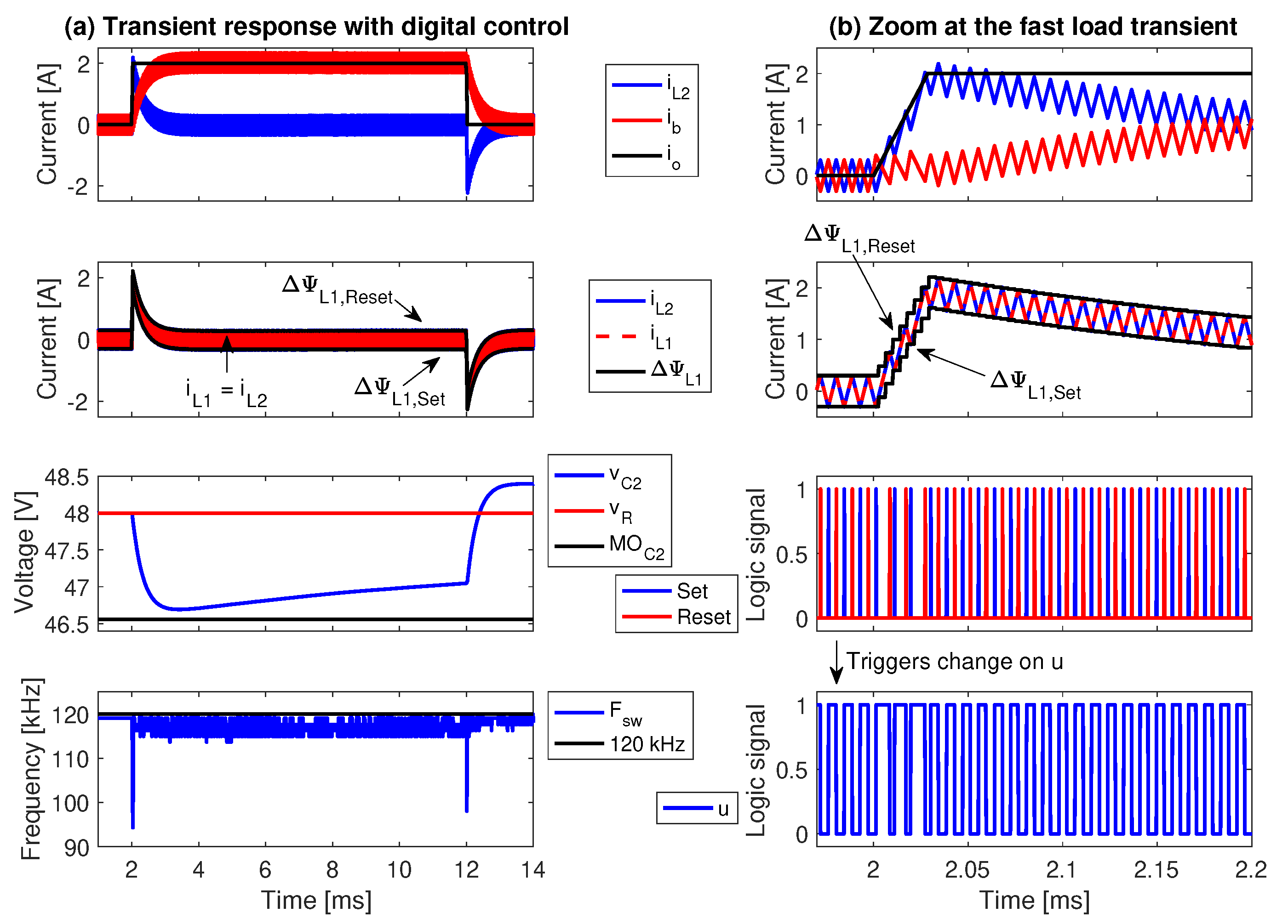
The simulation of this digital implementation, reported in Figure 10, evaluates the compensation of a load transient from steady state to battery charge with the maximum current derivative d i o d t = 70 A/ms; hence, it reproduces the conditions considered for the simulation of the analog implementation reported in Figure 5. The new simulation results of Figure 10a show two fast current transients between 0 A and 2 A, where the Zeta converter provides the fast current components, as expected. The stable condition i L 1 = i L 2 is also confirmed in this simulation, where i L 1 is constrained by Ψ L 1 , S e t and Ψ L 1 , R e s e t , thus ensuring the global stability of the SMC, as given in inequality (54). In addition, the C 2 voltage is constrained to the M O C 2 limit, demonstrating that the SMC’s digital implementation provides the same performance of the analog implementation. Finally, the switching frequency is always below the maximum design limit ( 120 kHz), thus requiring the same MOSFETs used for the analog implementation of the SMC.
Figure 10b shows a zoom of this simulation, which confirms that the Zeta converter provides the high-frequency component of the load current transient. The zoom also shows the detail of Ψ L 1 , S e t and Ψ L 1 , R e s e t , where the discretization caused by the sampling frequency of Thread 1 (264 kSPS) is observed. This simulation also shows the correct operation of the modified formulation of the sliding surface given in inequality (54), and it reports both the S e t and R e s e t signals generated by the CMPSS, where S e t = 1 S e t ¯ . Finally, the control signal u generated by Thread 2 is also presented, which agrees with the modified control law.
In summary, the simulations of both the analog and digital implementations of the SMC confirm the correct operation of the power system and the adaptive SMC for any operation condition. Therefore, the proposed solution can supply the current transients imposed by the load, thus forcing the battery to supply only low-frequency components. In addition, it was demonstrated that both analog and digital implementations of the adaptive SMC exhibit equivalent performances; hence, the one more suitable for the particular application can be adopted.

5.3. Comparison with a Classical Controller

This subsection presents the design of a cascade structure based on PI controllers to provide a comparison with a classical solution. The first step is to obtain the small-signal model of the power stage as X ˙ = A m × X + B m × U x , where X = i L 1 i L 2 v C 1 v C 2 T is the state vector, U x = d v b T is the input vector, A m is the state Jacobian and B m is the input Jacobian. This process is performed by deriving the differential equations given in (14)–(17), as described in [40], obtaining the following Jacobian matrices:
A m = 0 0 1 d L 1 d L 1 0 0 d L 2 d L 2 1 d C 1 d C 1 0 0 d C 2 d C 2 0 0 B m = v C 1 + v C 2 L 1 0 v C 1 + v C 2 L 2 1 L 2 i L 1 + i L 2 C 1 0 i L 1 + i L 2 C 2 0
The output of the small-signal model is calculated from Y = C m × X + D m × U x , where C m and D m relate the output with the states and the inputs, respectively. The output of the small-signal model is Y = i L 2 because i L 2 must be regulated to follow the i R value provided by the high-pass filter; hence, C m = 0 1 0 0 and D m = 0 0 .
The steady-state values of d, i L 1 , i L 2 , v C 1 and v C 2 are calculated from Equations (18)–(20) and replaced into Jacobians (59), and such a numerical small-signal model is introduced into the sisotool function of Matlab to design a PI controller; in [40], such a design is implemented using the classical root-locus technique. The design of that PI controller considers a damping ratio equal to 0.707 and a closed-loop bandwidth equal to F s w / 10 , which are standard criteria for linearized models; the resulting controller was G P I , c = 0.1616 · s + 4.125 × 10 4 s . Finally, this G P I c controller processes the error between i R and i L 2 to produce the duty cycle of an additional PWM circuit used to generate the MOSFET signals; Figure 11 shows the structure of this inner current loop.
The v C 2 voltage is also regulated with a PI controller named G P I , v . Such a second PI controller processes the error between v C 2 and the reference v R to produce the additional changes on i L 2 needed to regulate v C 2 with the desired settling time. This cascade controller requires a closed-loop model of the inner current loop. Equation (17) describes the dynamic behavior of v C 2 with respect to the inductor currents, where the inner current loop guarantees the current relation given in Equation (20); hence, the resulting closed-loop model is given in both time domain (60) and Laplace domain (61).
d v C 2 d t = d 1 d · i L 2 C 2
v C 2 i L 2 = d 1 d · 1 C 2 · s
The design of the voltage PI controller ( G P I , v ) was performed using Equation (61) for a unitary damping ratio to avoid any voltage oscillation and to request a slow current profile to the battery, thus avoiding high-frequency transients. In addition, the controller was designed to impose the desired settling time t s , C 2 = 100 ms, which results in the controller G P I , v = 0.055 · s + 29.412 s designed with the sisotool function of Matlab.
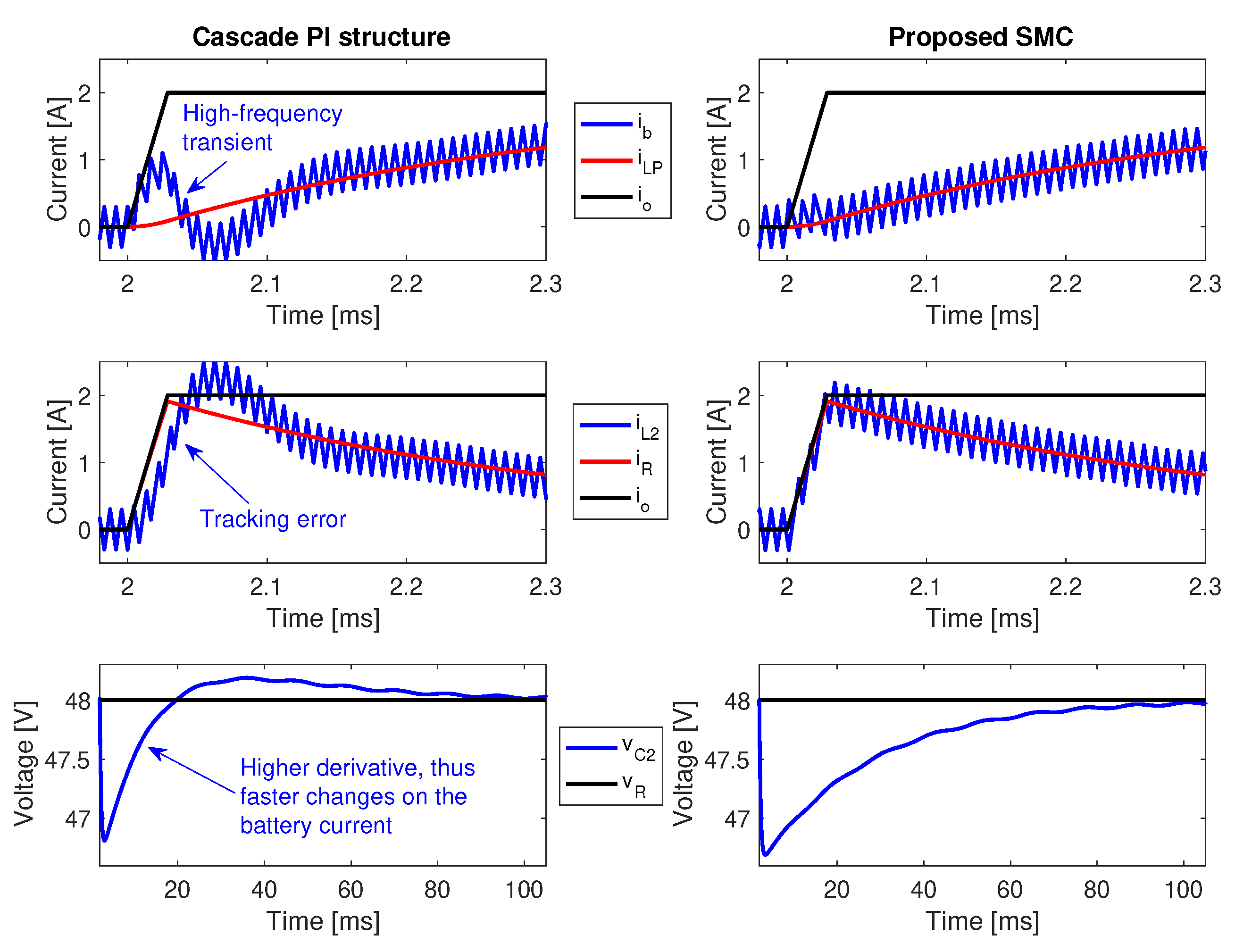
The control structure of Figure 11 was implemented in PSIM, and the performances of both the classical solution (cascade PI structure) and proposed SMC were contrasted. Figure 12 shows the circuital simulation of both solutions, where the proposed SMC (right side) imposes the desired low-frequency behavior i L P = i o i R on the battery current; instead, the cascade PI structure (left side) introduces an undesired high-frequency transient to the battery current. This undesired behavior is caused by the tracking error of G P I , c observed in i L 2 for the cascade PI structure, which is the result of the bandwidth limitation introduced in the linearization process; moreover, i L 2 also exhibits an overshoot caused by the change on the operation point. Instead, the proposed SMC forces i L 2 to track i R with null error, thus ensuring the desired low-frequency behavior of the battery current.
Figure 12 also presents, in the bottom waveforms, the behavior of v C 2 for both controllers. The v C 2 waveform imposed by the proposed SMC has the desired M O C 2 and t s , C 2 without any overshoot, thus requesting a low-frequency current in the battery in order to restore the energy in C 2 . Instead, the G P I , v controller from the cascade PI structure, despite being designed with a unitary damping ratio, cannot avoid the voltage overshoot. In addition, G P I , v imposes a higher derivative, thus requiring faster changes to the battery current, which is an undesired battery condition.
The analog implementation of the cascade PI structure requires two adders, two PI controllers formed by two integrators, two gains and two adders, and a PWM circuit formed by a comparator, a triangular waveform generator and an adder. The analog implementation of the proposed SMC, depicted in Figure 4, requires four adders, two dividers, a multiplier, and a gain; the SMC control circuit is formed by two comparators and an S-R flip-flop. Therefore, the proposed SMC requires integrated circuits for multiplication and division operations, while the cascade PI structure requires analog integrators. Thus, the analog implementation complexity of both controllers is similar. The digital implementation of the cascade PI structure also requires two threads, one for the inner current loop and another for the voltage loop. In addition, a complementary PWM peripheral must be used to produce both control signals. Hence, it has a complexity similar to the digital implementation of the proposed SMC reported in Figure 8.
In conclusion, the proposed SMC performs better than a classical solution based on cascade PI controllers. This performance is observed in the tracking efficiency that ensures i L 2 = i R , which imposes the desired low-frequency performance in the battery. Finally, the implementation complexity of both solutions is similar since both control solutions can be implemented using a few integrated circuits.

6. Conclusions

This paper presented an algorithm for designing both the power and control stages of a HESS based on a bidirectional Zeta converter, a battery, and a capacitor. The designed adaptive sliding-mode controller, which can be implemented on a low-cost platform, guarantees a safe battery current, which prevents distortion of the DC bus voltage waveform and avoids high-frequency transients that could reduce the battery’s lifespan. Moreover, the implementation of the adaptive sliding-mode controller is presented in detail using analog and digital circuits. An application example, where the battery was both charged and discharged, confirmed that during fast current transients, the Zeta converter provided the fast current components, while the battery responded with slow current derivatives. In addition, the switching function remained within the hysteresis band, ensuring the global stability of the adaptive sliding-mode controller. Finally, a comparison with a classical cascade PI structure demonstrated that the proposed adaptive controller provided superior performance, as evidenced by the tracking efficiency, which ensures that the inductor current matches the reference current, thus imposing the desired low-frequency performance on the battery.

Author Contributions

Conceptualization, A.T., C.A.R.-P., M.L.O.-G., A.J.S.-M. and S.I.S.-G.; Methodology, A.T., C.A.R.-P., M.L.O.-G., A.J.S.-M. and S.I.S.-G.; Formal analysis, A.T., C.A.R.-P., M.L.O.-G., A.J.S.-M. and S.I.S.-G.; Investigation, A.T., C.A.R.-P., M.L.O.-G., A.J.S.-M. and S.I.S.-G.; Writing—review & editing, A.T., C.A.R.-P., M.L.O.-G., A.J.S.-M. and S.I.S.-G. All authors have read and agreed to the published version of the manuscript.

Funding

This research was funded by Instituto Tecnológico Metropolitano, Universidad Nacional de Colombia, Universidad del Valle, and Minciencias—Ministerio de Ciencia Tecnología e Innovación of Colombia under project “Estrategias de dimensionamiento, planeación y gestión inteligente de energía a partir de la integración y la optimización de las fuentes no convencionales, los sistemas de almacenamiento y cargas eléctricas, que permitan la generación de soluciones energéticas confiables para los territorios urbanos y rurales de Colombia”, with Minciencias code 71148, inside the research program RC80740-178-2021, Hermes code 46771, and Sicop code CI21154.

Data Availability Statement

Data are contained within the article.

Conflicts of Interest

The authors declare no conflicts of interest.

References

  1. Sun, Y.N.; Zhuang, Z.L.; Xu, H.W.; Qin, W.; Feng, M.J. Data-driven modeling and analysis based on complex network for multimode recognition of industrial processes. J. Manuf. Syst. 2022, 62, 915–924. [Google Scholar] [CrossRef]
  2. Van De Berg, D.; Savage, T.; Petsagkourakis, P.; Zhang, D.; Shah, N.; Del Rio-Chanona, E.A. Data-driven optimization for process systems engineering applications. Chem. Eng. Sci. 2022, 248, 117135. [Google Scholar] [CrossRef]
  3. Liu, S.; Cheng, H. Manufacturing Process Optimization in the Process Industry. Int. J. Inf. Technol. Web Eng. 2024, 19, 1–20. [Google Scholar] [CrossRef]
  4. Ghahramani, M.; Qiao, Y.; Zhou, M.C.; O’Hagan, A.; Sweeney, J. AI-based modeling and data-driven evaluation for smart manufacturing processes. IEEE/CAA J. Autom. Sin. 2020, 7, 1026–1037. [Google Scholar] [CrossRef]
  5. Cerda-Flores, S.C.; Rojas-Punzo, A.A.; Nápoles-Rivera, F. Applications of Multi-Objective Optimization to Industrial Processes: A Literature Review. Processes 2022, 10, 133. [Google Scholar] [CrossRef]
  6. Dey, S.; Gupta, N.; Pathak, S.; Kela, D.H.; Datta, S. Data-Driven Design Optimization for Industrial Products. In Optimization in Industry; Datta, S., Davim, J.P., Eds.; Series Title: Management and Industrial Engineering; Springer International Publishing: Cham, Switzerland, 2019; pp. 253–267. [Google Scholar] [CrossRef]
  7. Zhao, J.; Wang, W.; Sheng, C. Data-Driven Prediction for Industrial Processes and Their Applications; Information Fusion and Data Science; Springer International Publishing: Cham, Switzerland, 2018. [Google Scholar] [CrossRef]
  8. Aghmadi, A.; Mohammed, O.A. Energy Storage Systems: Technologies and High-Power Applications. Batteries 2024, 10, 141. [Google Scholar] [CrossRef]
  9. Abo-Khalil, A.G.; Sobhy, A.; Abdelkareem, M.A.; Olabi, A. Advancements and challenges in hybrid energy storage systems: Components, control strategies, and future directions. Int. J. Thermofluids 2023, 20, 100477. [Google Scholar] [CrossRef]
  10. Leon, J.I.; Dominguez, E.; Wu, L.; Marquez Alcaide, A.; Reyes, M.; Liu, J. Hybrid Energy Storage Systems: Concepts, Advantages, and Applications. IEEE Ind. Electron. Mag. 2021, 15, 74–88. [Google Scholar] [CrossRef]
  11. Salah, O.; Shamayleh, A.; Mukhopadhyay, S. Energy Management of a Multi-Source Power System. Algorithms 2021, 14, 206. [Google Scholar] [CrossRef]
  12. Emrani, A.; Berrada, A. A comprehensive review on techno-economic assessment of hybrid energy storage systems integrated with renewable energy. J. Energy Storage 2024, 84, 111010. [Google Scholar] [CrossRef]
  13. Monhof, M.; Beverungen, D.; Klör, B.; Bräuer, S. Extending Battery Management Systems for Making Informed Decisions on Battery Reuse. In New Horizons in Design Science: Broadening the Research Agenda; Donnellan, B., Helfert, M., Kenneally, J., VanderMeer, D., Rothenberger, M., Winter, R., Eds.; Series Title: Lecture Notes in Computer Science; Springer International Publishing: Cham, Switzerland, 2015; Volume 9073, pp. 447–454. [Google Scholar] [CrossRef]
  14. Lei, H.; Li, K.; Chong, B. A Review of Hybrid Energy Storage System for Heavy-Duty Electric Vehicle. Transp. Res. Procedia 2023, 70, 234–240. [Google Scholar] [CrossRef]
  15. Song, Z.; Hofmann, H.; Li, J.; Han, X.; Zhang, X.; Ouyang, M. A comparison study of different semi-active hybrid energy storage system topologies for electric vehicles. J. Power Sources 2015, 274, 400–411. [Google Scholar] [CrossRef]
  16. Lencwe, M.J.; Chowdhury, S.P.D.; Olwal, T.O. Hybrid energy storage system topology approaches for use in transport vehicles: A review. Energy Sci. Eng. 2022, 10, 1449–1477. [Google Scholar] [CrossRef]
  17. Hasan, M.K.; Mahmud, M.; Ahasan Habib, A.; Motakabber, S.; Islam, S. Review of electric vehicle energy storage and management system: Standards, issues, and challenges. J. Energy Storage 2021, 41, 102940. [Google Scholar] [CrossRef]
  18. Castaings, A.; Lhomme, W.; Trigui, R.; Bouscayrol, A. Practical control schemes of a battery/supercapacitor system for electric vehicle. IET Electr. Syst. Transp. 2016, 6, 20–26. [Google Scholar] [CrossRef]
  19. Shyni, R.; Kowsalya, M. HESS-based microgrid control techniques empowered by artificial intelligence: A systematic review of grid-connected and standalone systems. J. Energy Storage 2024, 84, 111012. [Google Scholar] [CrossRef]
  20. Atawi, I.E.; Al-Shetwi, A.Q.; Magableh, A.M.; Albalawi, O.H. Recent Advances in Hybrid Energy Storage System Integrated Renewable Power Generation: Configuration, Control, Applications, and Future Directions. Batteries 2022, 9, 29. [Google Scholar] [CrossRef]
  21. Wang, W.; Yuan, B.; Sun, Q.; Wennersten, R. Application of energy storage in integrated energy systems—A solution to fluctuation and uncertainty of renewable energy. J. Energy Storage 2022, 52, 104812. [Google Scholar] [CrossRef]
  22. Barelli, L.; Cardelli, E.; Pelosi, D.; Ciupageanu, D.A.; Ottaviano, P.A.; Longo, M.; Zaninelli, D. Energy from the Waves: Integration of a HESS to a Wave Energy Converter in a DC Bus Electrical Architecture to Enhance Grid Power Quality. Energies 2021, 15, 10. [Google Scholar] [CrossRef]
  23. Moreno, H.; Schaum, A. Low-Order Electrochemical State Estimation for Li-Ion Batteries. Algorithms 2023, 16, 73. [Google Scholar] [CrossRef]
  24. Liu, S.; Ling, R.; Feng, F. Equalization strategy for fast energy regulation of supercapacitor in hybrid energy storage system. J. Energy Storage 2023, 65, 107318. [Google Scholar] [CrossRef]
  25. Rahman, A.U.; Zehra, S.S.; Ahmad, I.; Armghan, H. Fuzzy supertwisting sliding mode-based energy management and control of hybrid energy storage system in electric vehicle considering fuel economy. J. Energy Storage 2021, 37, 102468. [Google Scholar] [CrossRef]
  26. Lencwe, M.J.; Olwal, T.O.; Chowdhury, S.D.; Sibanyoni, M. Nonsolitary two-way DC-to-DC converters for hybrid battery and supercapacitor energy storage systems: A comprehensive survey. Energy Rep. 2024, 11, 2737–2767. [Google Scholar] [CrossRef]
  27. Zimmermann, T.; Keil, P.; Hofmann, M.; Horsche, M.F.; Pichlmaier, S.; Jossen, A. Review of system topologies for hybrid electrical energy storage systems. J. Energy Storage 2016, 8, 78–90. [Google Scholar] [CrossRef]
  28. Ramu, S.K.; Vairavasundaram, I.; Palaniyappan, B.; Bragadeshwaran, A.; Aljafari, B. Enhanced energy management of DC microgrid: Artificial neural networks-driven hybrid energy storage system with integration of bidirectional DC-DC converter. J. Energy Storage 2024, 88, 111562. [Google Scholar] [CrossRef]
  29. Moghadam, M.; Ghaffarzadeh, N. Suppressing solar PV output fluctuations by designing an efficient hybrid energy storage system controller. Unconv. Resour. 2024, 4, 100077. [Google Scholar] [CrossRef]
  30. Srinivasan, C.; Sheeba Joice, C. Energy management of hybrid energy storage system in electric vehicle based on hybrid SCSO-RERNN approach. J. Energy Storage 2024, 78, 109733. [Google Scholar] [CrossRef]
  31. Guentri, H.; Allaoui, T.; Mekki, M.; Denai, M. Power management and control of a photovoltaic system with hybrid battery-supercapacitor energy storage based on heuristics methods. J. Energy Storage 2021, 39, 102578. [Google Scholar] [CrossRef]
  32. Erickson, R.W.; Maksimović, D. Fundamentals of Power Electronics; Springer International Publishing: Cham, Switzerland, 2020. [Google Scholar] [CrossRef]
  33. Perruquetti, W.; Barbot, J.P. Sliding Mode Control in Engineering; Marcel Dekker: New York, NY, USA, 2002; Volume 11. [Google Scholar]
  34. Sira-Ramirez, H. Sliding motions in bilinear switched networks. IEEE Trans. Circuits Syst. 1987, 34, 919–933. [Google Scholar] [CrossRef]
  35. Ogata, K. Modern Control Engineering, 5th ed.; eTextbook; Pearson: London, UK, 2021. [Google Scholar]
  36. Clayton, G.B.; Winder, S. Operational Amplifiers; Elsevier: Amsterdam, The Netherlands, 2003. [Google Scholar]
  37. Devices, A. 10 MHz, Four-Quadrant Multiplier/Divider AD734; Datasheet; Analog Device, Inc.: Norwood, MA, USA, 2011. [Google Scholar]
  38. Instruments, T. TMS320F2837xD Dual-Core Real-Time Microcontrollers; Datasheet; Texas Instruments, Inc.: Dallas, TX, USA, 2024. [Google Scholar]
  39. Paarmann, L.D. Design and Analysis of Analog Filters: A Signal Processing Perspective; Springer Science & Business Media: Berlin/Heidelberg, Germany, 2001; Volume 617. [Google Scholar]
  40. Petrone, G.; Ramos-Paja, C.A.; Spagnuolo, G. Photovoltaic Sources Modeling, 1st ed.; Wiley: Hoboken, NJ, USA, 2017. [Google Scholar] [CrossRef]
Figure 1. Structure of the hybrid energy storage system.
Algorithms 17 00319 g001
Figure 2. Zeta power system designed to support battery transients.
Algorithms 17 00319 g002
Figure 3. C 2 voltage and current ripple waveforms.
Algorithms 17 00319 g003
Figure 4. Analog implementation of the control algorithm.
Algorithms 17 00319 g004
Figure 5. Fast load transient to battery discharge.
Algorithms 17 00319 g005
Figure 6. Fast load transient to battery charge.
Algorithms 17 00319 g006
Figure 7. Consecutive perturbations and settling time.
Algorithms 17 00319 g007
Figure 8. Digital implementation of the control algorithm.
Algorithms 17 00319 g008
Figure 9. Flowchart of the digital implementation.
Algorithms 17 00319 g009
Figure 10. Response of the digital implementation to fast load transients.
Algorithms 17 00319 g010
Figure 11. Cascade PI structure.
Algorithms 17 00319 g011
Figure 12. Comparison with a cascade PI structure.
Algorithms 17 00319 g012
Table 1. Characteristics of some works on HESS.
Ref.Storage DeviceHESS TypeControl’s AlgorithmConverterComments
 [30]SC-baterryFully activeSCSO-RERNNBuck-boostEV application
 [29]SC-batteryFully activePI (battery), MPC (SC)BC not
specified
MG with PV
 [28]SC-batteryFully activeANNBuck-boostReferences’ generation
with ANN
 [31]SC-batteryFully activePIBuck-boostPI tunning with
LMI-PSO-GA.
 [25]SC-batteryFully activeSSMCBuck-boostReferences’ generation
with fuzzy logic
 [18]SC-batterySC Semi-activePIBoostEV application
Table 2. Characteristics of the application example.
DescriptionVariableValue
Battery voltage v b 48 V
Nominal C 2 voltage v R 48 V
Maximum deviation of C 2 voltage M O C 2 3 %
Settling time of C 2 voltage t s , C 2 100 ms
Maximum derivative in the load current max d i o d t 70 A/ms
Maximum load transient magnitude Δ i o 2 A
Maximum safe frequency for the battery F s a f e 500 Hz
Maximum switching frequency F s w 120 kHz
Table 3. Circuital parameters of the application example.
ParameterValueNominal ConditionEnergy Stored
L 1 330 μ H 0 A 0 Wh, 0 Ah
L 2 330 μ H 0 A 0 Wh, 0 Ah
C 1 470 μ F 48 V 0.15 mWh, 0.003 mAh
C 2 470 μ F 48 V 0.15 mWh, 0.003 mAh
Δ Ψ 0.3 A--
Disclaimer/Publisher’s Note: The statements, opinions and data contained in all publications are solely those of the individual author(s) and contributor(s) and not of MDPI and/or the editor(s). MDPI and/or the editor(s) disclaim responsibility for any injury to people or property resulting from any ideas, methods, instructions or products referred to in the content.