
Reduced Subthreshold Characteristics and Flicker Noise of an AlGaAs/InGaAs PHEMT Using Liquid Phase Deposited TiO2 as a Gate Dielectric


Abstract
:1. Introduction
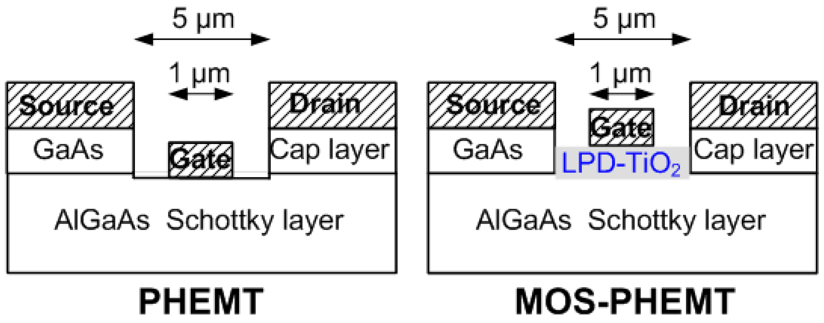
2. Experimental
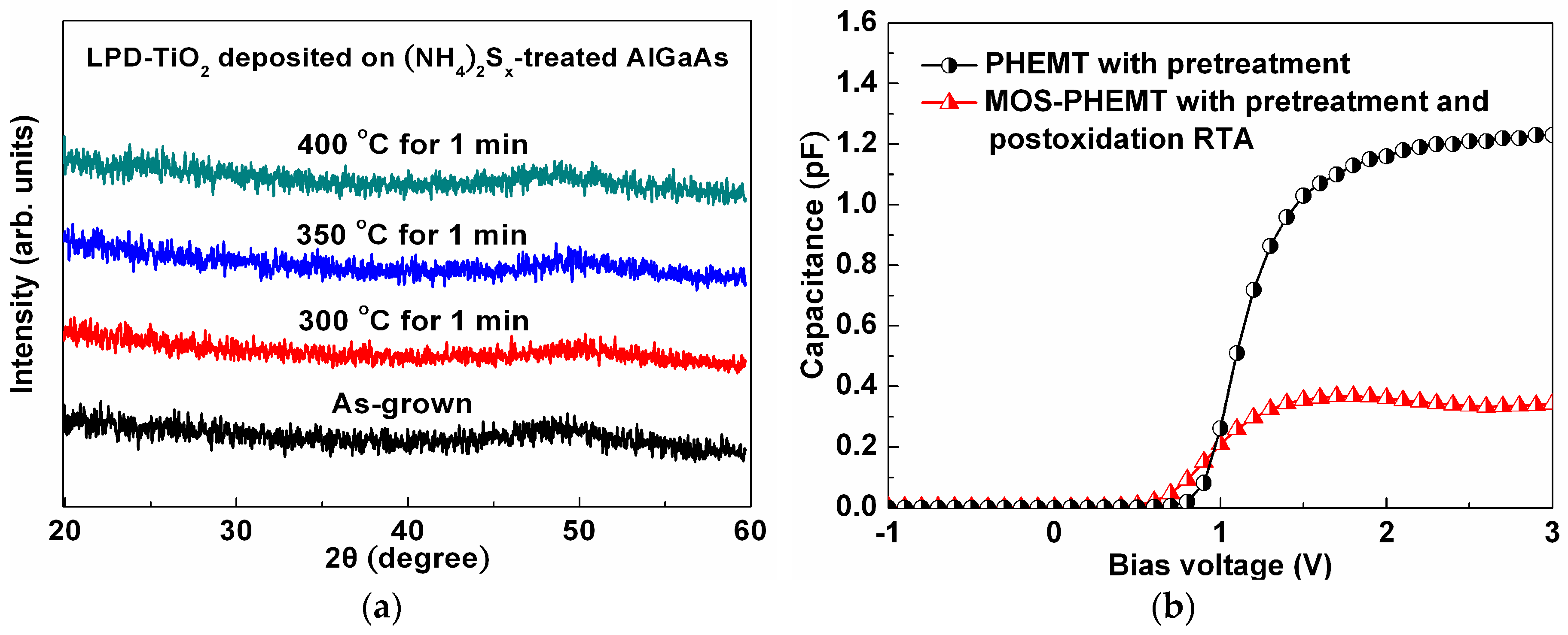
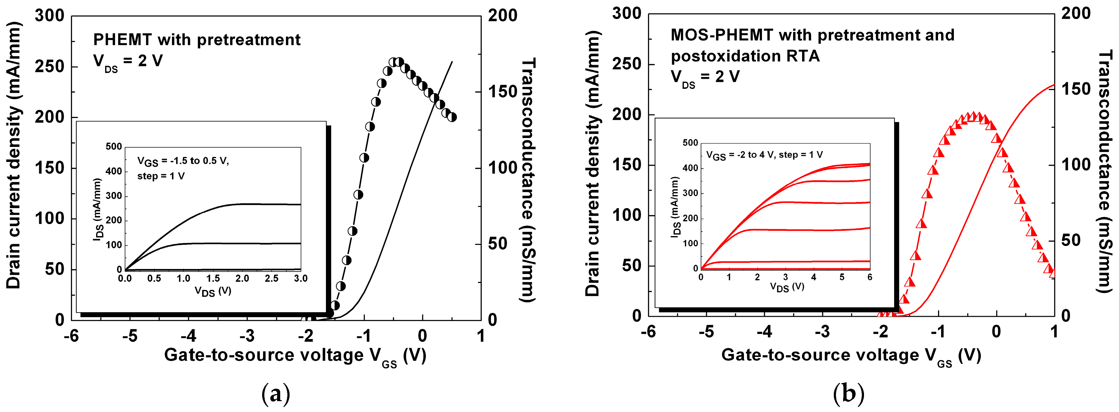
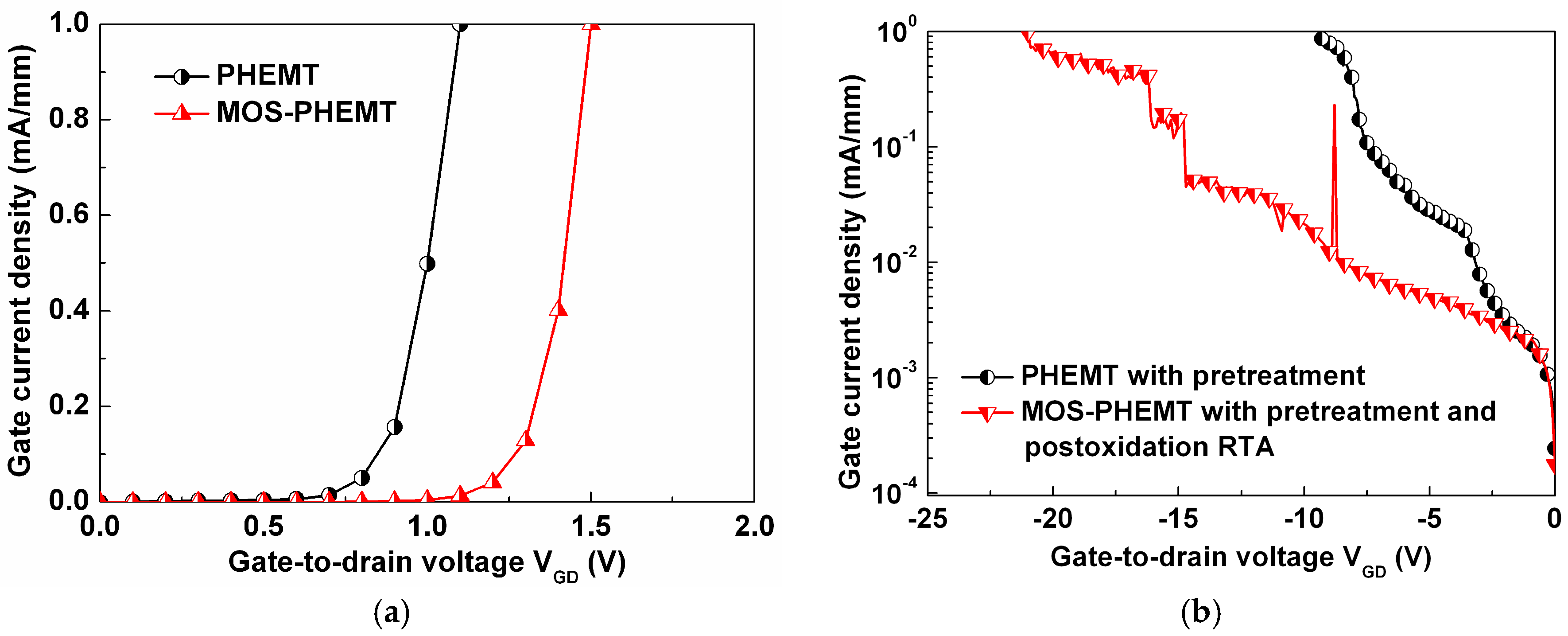
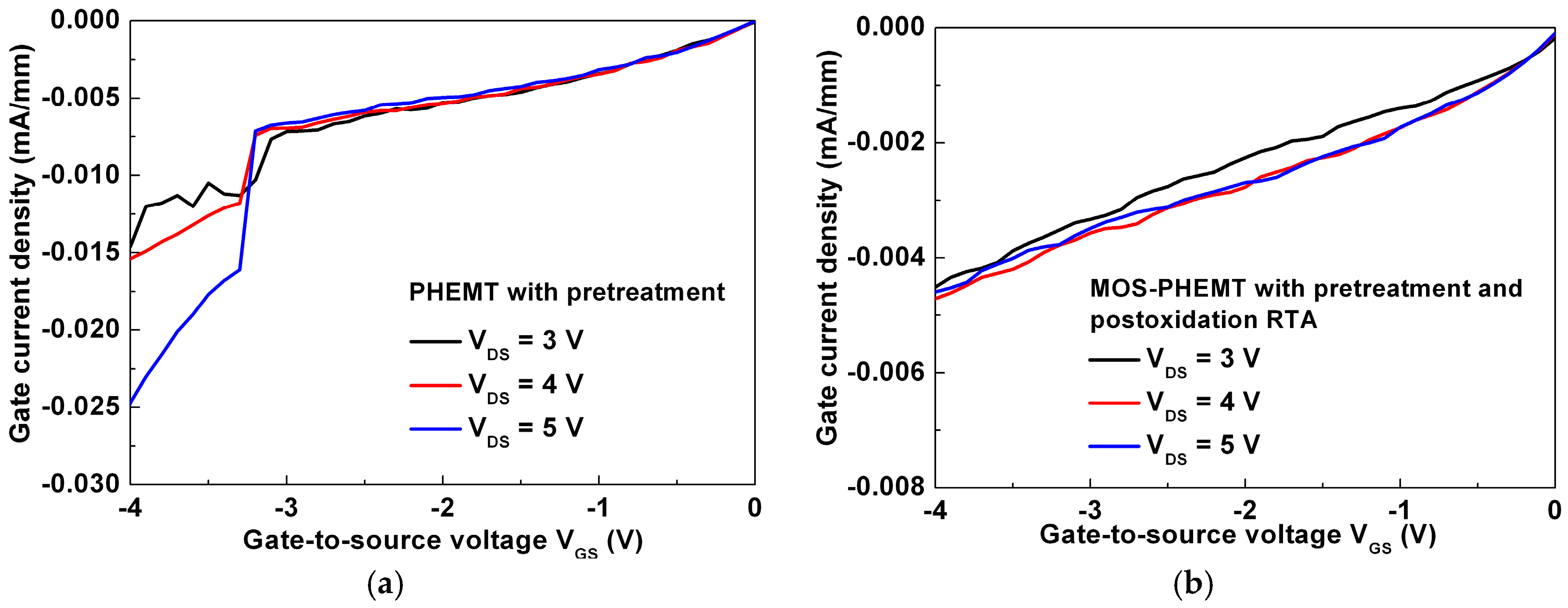
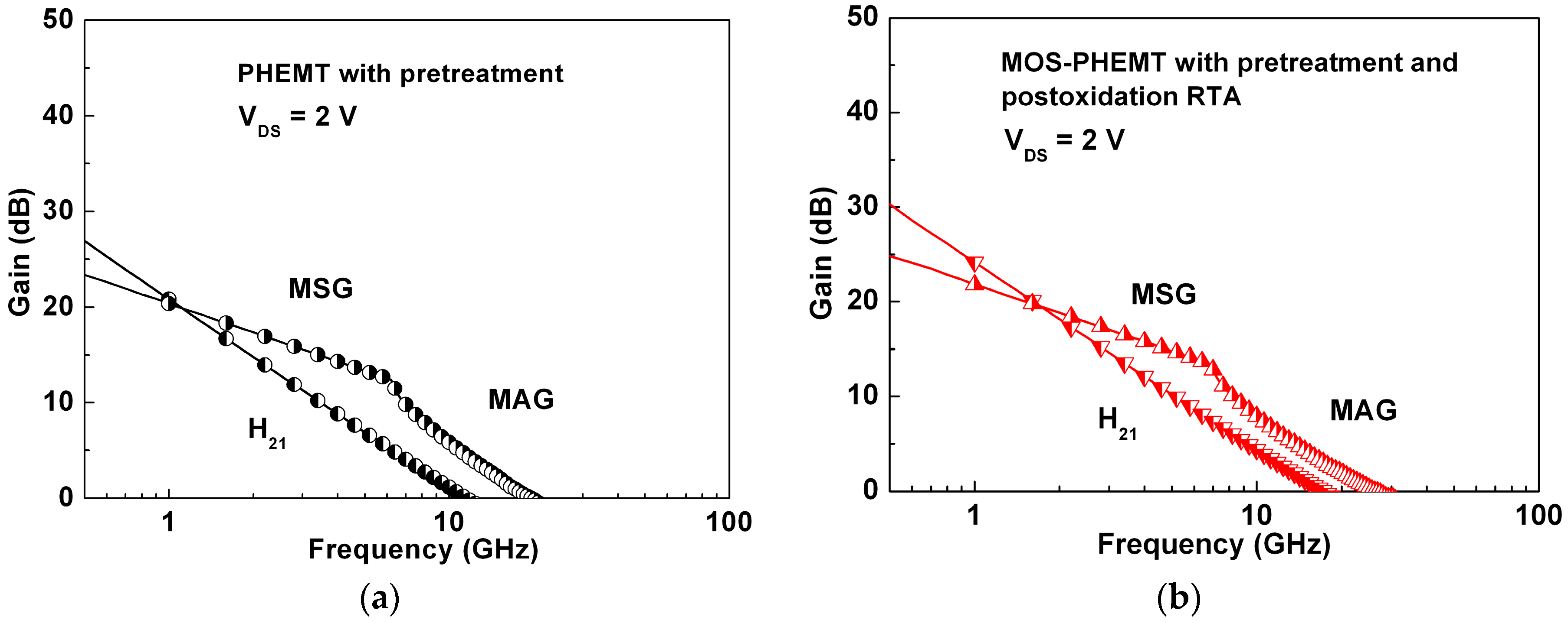
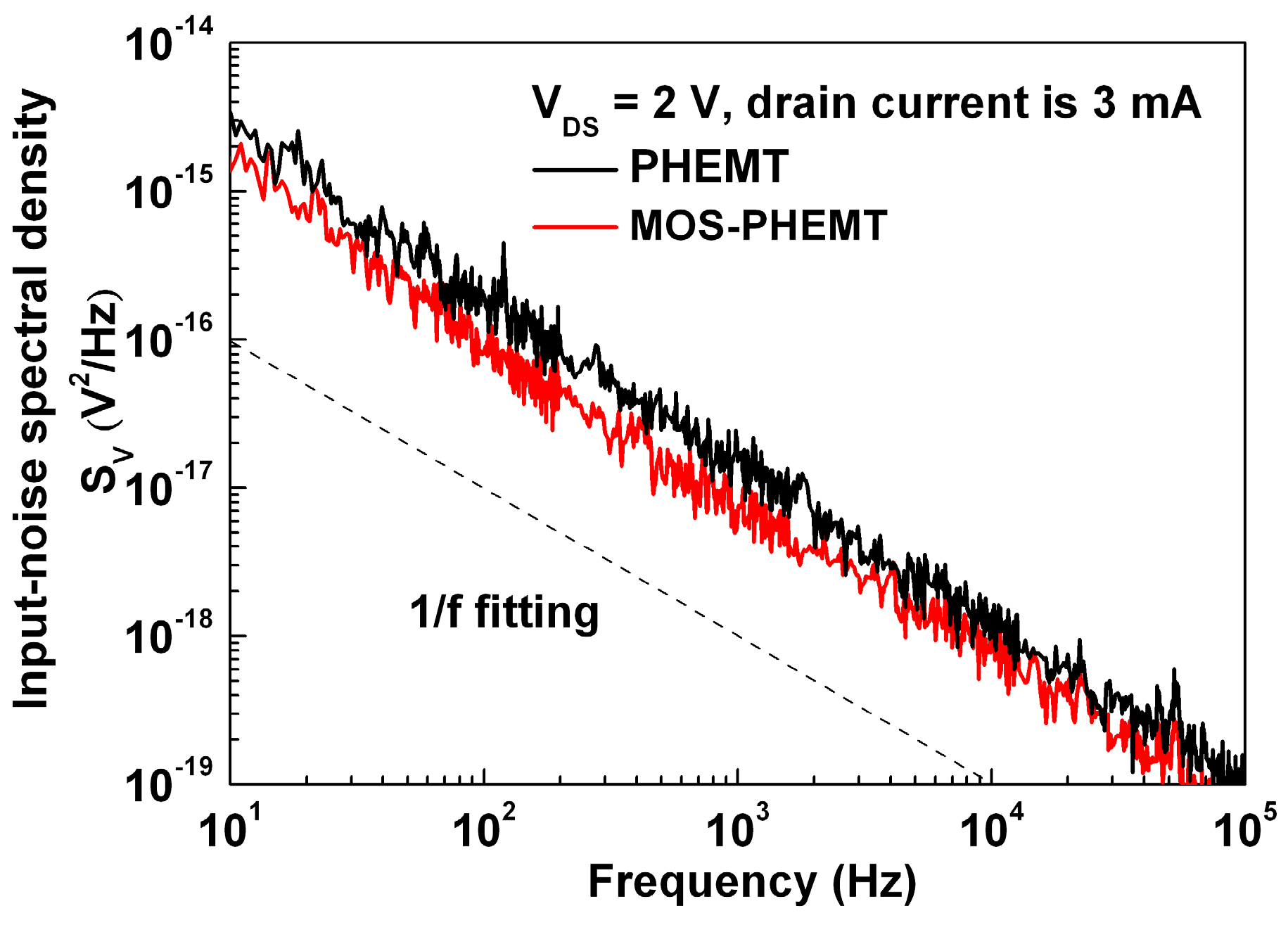
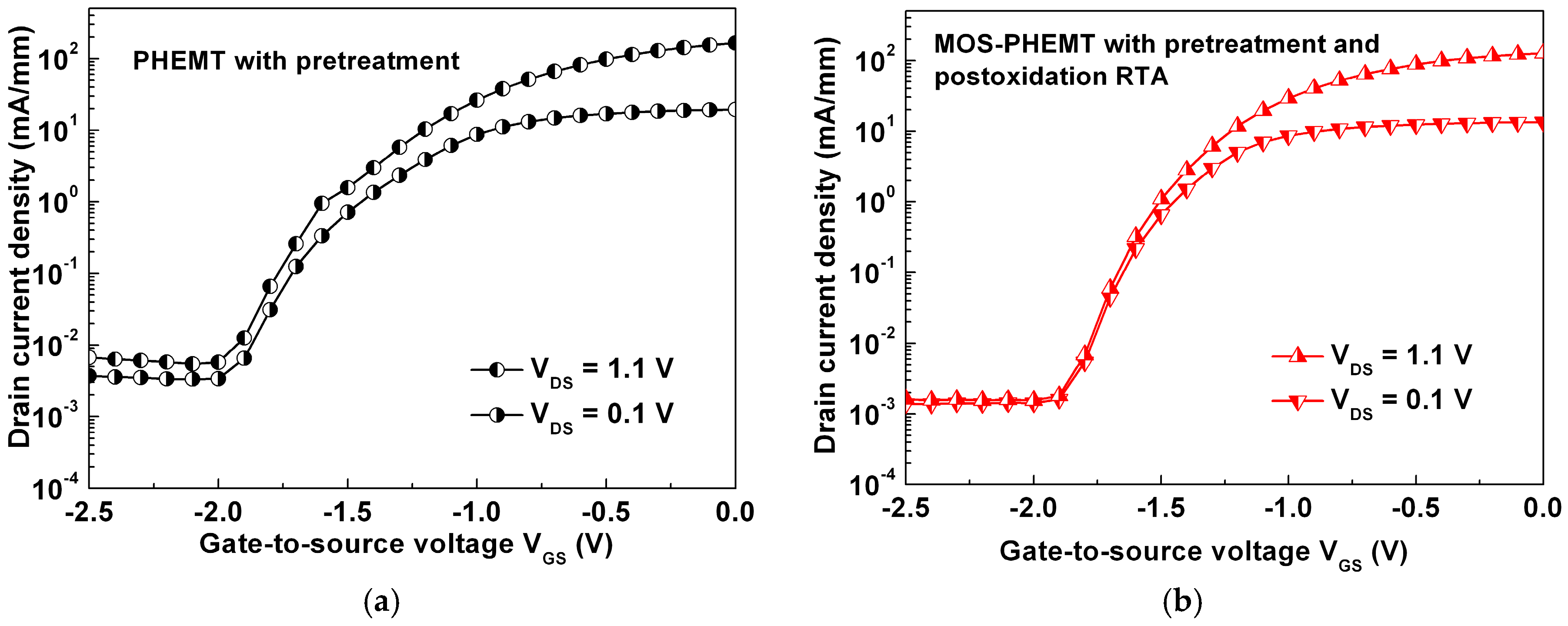
3. Results and Discussion
4. Conclusions
Acknowledgments
Author Contributions
Conflicts of Interest
References
- Lee, H.L.; Moon, S.M.; Dong, H.J.; Lee, M.Q.; Yu, J.W. K-band 0/180° Balanced Phase Shifter with DC-Offset Cancellation. Electron. Lett. 2013, 49, 1234–1235. [Google Scholar] [CrossRef]
- Lin, Y.S.; Wu, J.F.; Hsia, W.F.; Wang, P.C.; Chung, Y.H. Design of Electronically Switchable Single-to-Balanced Bandpass Low-Noise Amplifier. IET Microw. Antennas Propag. 2013, 7, 510–517. [Google Scholar] [CrossRef]
- Nikandish, G.; Babakrpur, E.; Medi, A.A. Harmonic Termination Technique for Single- and Multi-Band High-Efficiency Class-F MMIC Power Amplifiers. IEEE Trans. Microw. Theory Tech. 2014, 62, 1212–1220. [Google Scholar] [CrossRef]
- Ding, X.; Zhang, L. A High-Efficiency GaAs MMIC Power Amplifier for Multi-Standard System. IEEE Microw. Wirel. Compon. Lett. 2016, 26, 55–57. [Google Scholar] [CrossRef]
- Hartnagel, H.; Katilius, R.; Matulionis, A. Microwave Noise in Semiconductor Devices; John Wiley & Sons, Inc.: Hoboken, NJ, USA, 2001. [Google Scholar]
- Huang, H.K.; Wang, C.S.; Chang, C.P.; Wang, Y.H.; Wu, C.L.; Chang, C.S. Noise Characteristics of InGaP-gated PHEMTs under High Current and Thermal Accelerated Stresses. IEEE Trans. Electron. Devices 2005, 52, 1706–1712. [Google Scholar] [CrossRef]
- Yagi, S.; Shimizu, M.; Inaga, M.; Yamamoto, Y.; Piao, G.; Okumura, H.; Yano, Y.; Akutsu, N.; Ohashi, H. High Breakdown Voltage AlGaN/GaN MIS-HEMT with SiN and TiO2 Gate Insulator. Solid State Electron. 2006, 50, 1057–1061. [Google Scholar] [CrossRef]
- Hu, C.C.; Lin, M.S.; Wu, T.Y.; Adriyanto, F.; Sze, P.W.; Wu, C.L.; Wang, Y.H. AlGaN/GaN Metal-Oxide-Semiconductor High-Electron Mobility Transistor with Liquid-Phase-Deposited Barium-Doped TiO2 as a Gate Dielectric. IEEE Trans. Electron. Devices 2012, 59, 121–127. [Google Scholar] [CrossRef]
- Choi, W.; Seok, O.; Ryu, H.; Cha, H.Y.; Seo, K.S. High-Voltage and Low-Leakage-Current Gate Recessed Normally-Off GaN MIS-HEMTs with Dual Gate Insulator Employing PEALD-SiNx/RF-Sputtered-HfO2. IEEE Electron. Device Lett. 2014, 35, 175–177. [Google Scholar] [CrossRef]
- Yokozawa, M.; Iwasa, H.; Teramoto, I. Vapor Deposition of TiO2. Jpn. J. Appl. Phys. 1967, 7, 96–97. [Google Scholar] [CrossRef]
- Ha, H.K.; Yoshimoto, M.; Koinuma, H.; Moon, B.K.; Ishiwara, H. Open Air Plasma Chemical Vapor Deposition of Highly Dielectric Amorphous TiO2 Films. Appl. Phys. Lett. 1996, 68, 2965–2967. [Google Scholar] [CrossRef]
- Martin, N.; Rousselot, C.; Savall, C.; Palmino, F. Characterizations of Titanium Oxide Films Prepared by Radio Frequency Magnetron Sputtering. Thin Solid Films 1996, 287, 154–163. [Google Scholar] [CrossRef]
- Yang, T.S.; Shiu, C.B.; Wong, M.S. Structure and Hydrophilicity of Titanium Oxide Films Prepared by Electron Beam Evaporation. Surf. Sci. 2004, 548, 75–82. [Google Scholar] [CrossRef]
- Sonawane, R.S.; Hegde, S.G.; Dongare, M.K. Preparation of Titanium (IV) Oxide Thin Film Photocatalyst by Sol-Gel Dip Coating. Mater. Chem. Phys. 2003, 77, 744–750. [Google Scholar] [CrossRef]
- Wang, X.P.; Yu, Y.; Hu, X.F.; Gao, L. Hydrophilicity of TiO2 Films Prepared by Liquid Phase Deposition. Thin Solid Films 2000, 371, 148–152. [Google Scholar] [CrossRef]
- Lee, M.K.; Huang, J.J.; Shih, C.M.; Cheng, C.C. Properties of TiO2 Thin Films on InP Substrate Prepared by Liquid Phase Deposition. Jpn. J. Appl. Phys. 2002, 41, 4689–4690. [Google Scholar] [CrossRef]
- Lee, M.K.; Lee, H.C.; Hsu, C.M. High Dielectric Constant TiO2 Film Grown on Polysilicon by Liquid Phase deposition. Mater. Sci. Semicond. Process. 2007, 10, 61–67. [Google Scholar] [CrossRef]
- Mallak, M.; Bockmeyer, M.; Löbmann, P. Liquid Phase Deposition of TiO2 on Glass: Systematic Comparison to Films Prepared by Sol-Gel Processing. Solid State Electron. 2007, 515, 8072–8077. [Google Scholar] [CrossRef]
- Wu, T.Y.; Lin, S.K.; Sze, P.W.; Huang, J.J.; Chien, W.C.; Hu, C.C.; Tsai, M.J.; Wang, Y.H. AlGaN/GaN MOSHEMTs with Liquid-Phase-Deposited TiO2 as Gate Dielectric. IEEE Trans. Electron. Devices 2009, 56, 2911–2916. [Google Scholar] [CrossRef]
- Lee, K.W.; Huang, J.S.; Lu, Y.L.; Lee, F.M.; Lin, H.C.; Wu, T.Y.; Wang, Y.H. Investigation of TiO2 on AlGaAs Prepared by Liquid Phase Deposition and Its Application. Solid State Electron. 2011, 68, 85–89. [Google Scholar] [CrossRef]
- Huang, J.S.; Lee, T.L.; Zou, Y.J.; Lee, K.W.; Wang, Y.H. Sulfide Pretreatment Effects of Liquid Phase deposited TiO2 on AlGaAs and Its Application. Vacuum 2015, 118, 100–103. [Google Scholar] [CrossRef]
- Hu, C.C.; Lee, T.L.; Zou, Y.J.; Lee, K.W.; Wang, Y.H. Postoxidation Thermal Annealing Effects of Liquid Phase Deposited TiO2 on (NH4)2Sx-treated AlGaAs. Thin Solid Films 2014, 563, 40–43. [Google Scholar] [CrossRef]
- Chung, J.W.; Roberts, J.C.; Piner, E.L.; Palacios, T. Effect of Gate Leakage in the Subthreshold Characteristics of AlGaN/GaN HEMTs. IEEE Electron. Device Lett. 2008, 29, 1196–1198. [Google Scholar] [CrossRef]
- Suemitsu, T.; Enoki, T.; Sano, N.; Tomizawa, M.; Ishii, Y. An Analysis of the Kink Phenomena in InAlAs/InGaAs HEMT’s Using Two-Dimensional Device Simulation. IEEE Trans. Electron. Devices 1998, 45, 2390–2399. [Google Scholar] [CrossRef]
- Wang, H.; Liu, Y.; Zeng, R.; Tan, C.L. Understanding of the Excess Channel Noise in InAlAs/InGaAs/InPHigh Electron Mobility Transistors in Impact Ionization Regime. Appl. Phys. Lett. 2007, 90, 103503. [Google Scholar] [CrossRef]
- Lee, K.W.; Chen, W.S. Improved Low-Frequency Noise and Microwave Performance of Enhancement-Mode InGaP/InGaAs PHEMT with a Liquid-Phase Oxidized GaAs without a Gate Recess. ECS Solid State Lett. 2012, 2, Q9–Q11. [Google Scholar] [CrossRef]
- Hughes, B.; Fernandez, N.G.; Gladstone, J.M. GaAs FET’s with a Flicker-Noise Corner below 1 MHz. IEEE Trans. Electron. Devices 1987, 34, 733–741. [Google Scholar] [CrossRef]
- Lee, K.W. Improved Impact Ionization in AlGaAs/InGaAs PHEMT with a Liquid Phase Deposited SiO2 as the Gate Dielectric. ECS J. Solid State Sci. Technol. 2012, 2, Q27–Q29. [Google Scholar] [CrossRef]
- Basu, S.; Singh, P.K.; Sze, P.W.; Wang, Y.H. AlGaAs/InGaAs Metal-Oxide-Semiconductor Pseudomorphic High-Electron-Mobility Transistor with Low Temperature Liquid Phase DepositedAl2O3Gate Insulator. J. Appl. Phys. 2008, 104, 054116. [Google Scholar] [CrossRef]
- Lee, K.W.; Sze, P.W.; Wang, Y.H.; Houng, M.P. AlGaAs/InGaAs Metal-Oxide-Semiconductor Pseudomorphic High-Electron-Mobility Transistor with a Liquid Phase Oxidized AlGaAs as Gate Dielectric. Solid State Electron. 2005, 49, 213–217. [Google Scholar] [CrossRef]


| Group | This Work | [28] | [29] | [30] |
|---|---|---|---|---|
| Mode | D-mode | D-mode | D-mode | D-mode |
| Gate oxide | TiO2 | SiO2 | Al2O3 | Oxidized AlGaAs |
| Oxidation method | LPD | LPD | LPD | LPO |
| Temperature (°C) | 40 | 40 | 40 | 50 |
| Gate length (μm) | 1 | 1 | 1 | 1 |
| Maximum VGS (V) | 4 | 4 | 2.5 | 4 |
| Maximum IDS (mA/mm) | 420 | 421 | 433 | 380 |
| Gate voltage swing (V) | 0.8 | 2.5 | 2 | 0.7 |
| SubthresholdSwing (mV/dec) | 120–125 | 125–165 | – | – |
| SV at 10 Hz (V2·Hz−1) | 1.4 × 10⁻¹⁵ | – | – | – |
| fmax (GHz) | 26.4 | – | – | – |
© 2016 by the authors; licensee MDPI, Basel, Switzerland. This article is an open access article distributed under the terms and conditions of the Creative Commons Attribution (CC-BY) license (http://creativecommons.org/licenses/by/4.0/).
Share and Cite
Lam, K.-Y.; Huang, J.-S.; Zou, Y.-J.; Lee, K.-W.; Wang, Y.-H. Reduced Subthreshold Characteristics and Flicker Noise of an AlGaAs/InGaAs PHEMT Using Liquid Phase Deposited TiO2 as a Gate Dielectric. Materials 2016, 9, 861. https://doi.org/10.3390/ma9110861
Lam K-Y, Huang J-S, Zou Y-J, Lee K-W, Wang Y-H. Reduced Subthreshold Characteristics and Flicker Noise of an AlGaAs/InGaAs PHEMT Using Liquid Phase Deposited TiO2 as a Gate Dielectric. Materials. 2016; 9(11):861. https://doi.org/10.3390/ma9110861
Chicago/Turabian StyleLam, Kai-Yuen, Jung-Sheng Huang, Yong-Jie Zou, Kuan-Wei Lee, and Yeong-Her Wang. 2016. "Reduced Subthreshold Characteristics and Flicker Noise of an AlGaAs/InGaAs PHEMT Using Liquid Phase Deposited TiO2 as a Gate Dielectric" Materials 9, no. 11: 861. https://doi.org/10.3390/ma9110861
APA StyleLam, K.-Y., Huang, J.-S., Zou, Y.-J., Lee, K.-W., & Wang, Y.-H. (2016). Reduced Subthreshold Characteristics and Flicker Noise of an AlGaAs/InGaAs PHEMT Using Liquid Phase Deposited TiO2 as a Gate Dielectric. Materials, 9(11), 861. https://doi.org/10.3390/ma9110861