Review

Bi2Te3-Based Thermoelectric Films Fabricated by Magnetron Sputtering
College of Materials Science and Engineering, Nanjing Tech University, Nanjing 210009, China
*
Author to whom correspondence should be addressed.
Materials 2026, 19(10), 2111; https://doi.org/10.3390/ma19102111
Submission received: 17 April 2026 / Revised: 9 May 2026 / Accepted: 14 May 2026 / Published: 17 May 2026

Abstract

Bi2Te3-based materials are benchmark room-temperature thermoelectrics, widely used in refrigeration, waste heat recovery, and microdevice thermal management. Magnetron sputtering demonstrates significant potential as an effective strategy for the mass production of superior Bi2Te3 thin films, offering advantages such as dense microstructure, controllable composition, good repeatability, and compatibility with semiconductor processes. However, existing studies largely focus on individual factors affecting film properties, lacking a systematic understanding of the interrelationships among process parameters, microstructures, and thermoelectric performance. Poor comparability across studies due to varying deposition conditions further limits insight into key controlling mechanisms. Recent efforts have centered on three regulatory aspects in magnetron sputtering: (1) optimization of sputtering parameters (e.g., power, pressure, temperature, and target composition); (2) post-annealing treatment; and (3) doping modification. Notable progress has been made in enhancing thermoelectric performance through these approaches. This paper provides a comprehensive overview of recent advancements in the fabrication of Bi2Te3 thin films via magnetron sputtering, focusing on how process parameters, post-treatment, and doping affect microstructure, stoichiometry, and thermoelectric properties. The aim is to elucidate structure-performance correlations and guide the optimized preparation of high-performance films.

1. Introduction

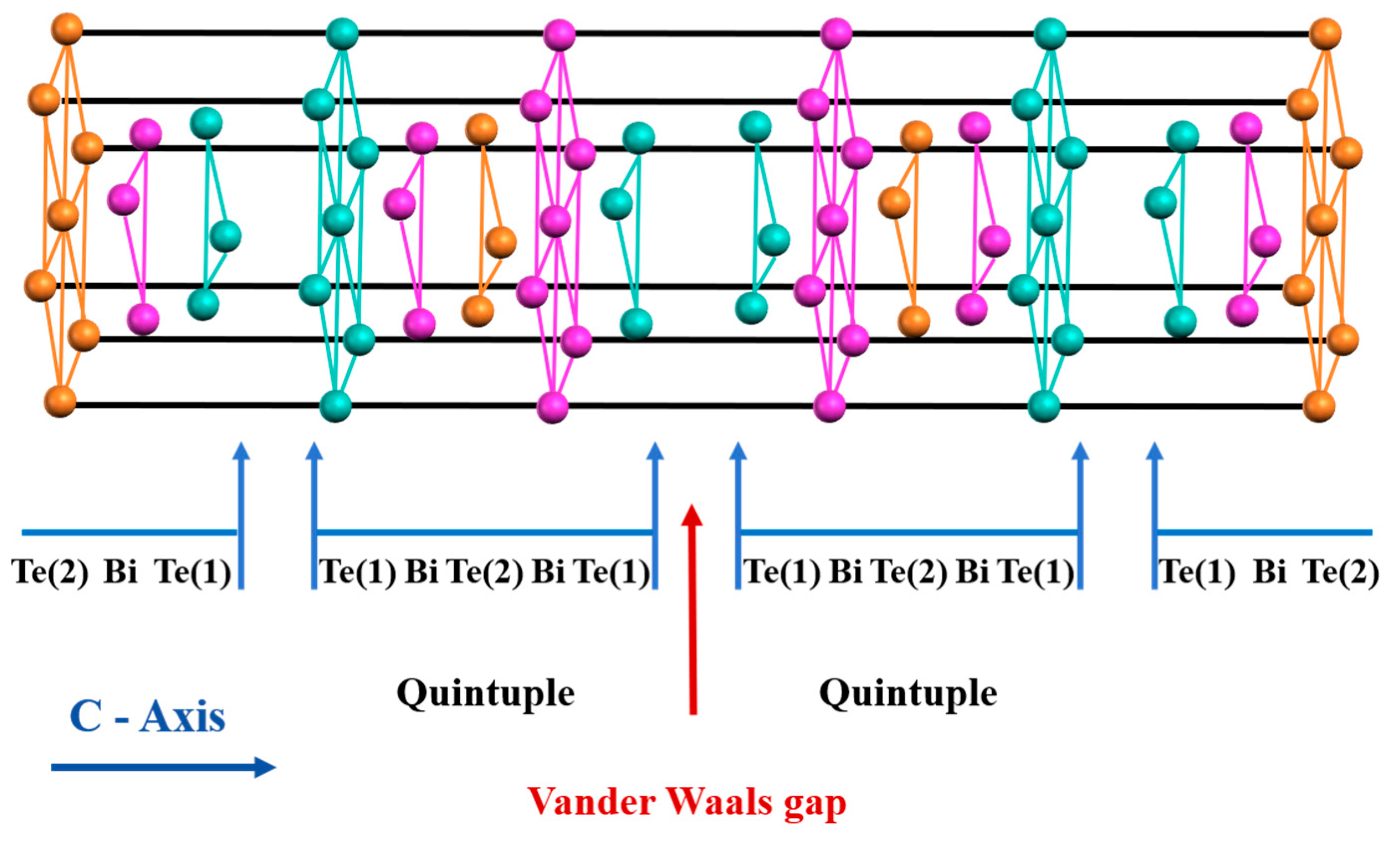
At present, Bi2Te3-based compounds and their solid solutions represent the premier thermoelectric materials operating around room temperature, playing an essential role in both solid-state cooling and waste heat harvesting technologies [1,2]. At ambient conditions, the VVI semiconductor Bi2Te3 crystallizes in a rhombohedral lattice (space group R 3 ¯ m). As depicted in Figure 1, its structural framework is defined by the c-axis stacking of Te(1)-Bi-Te(2)-Bi-Te(1) quintuple layers (QLs), which are connected exclusively through weak van der Waals interactions, and this unique crystal structure leads to significant anisotropy in its thermoelectric transport properties [3,4]. Bi2Te3 is a narrow bandgap semiconductor with a bandgap of ~0.145 eV and carrier concentration between 1018 and 1019 cm−3. Through doping with elements such as Se or halogens to achieve n-type behavior, alongside Sb for p-type doping, ensuring the successful synthesis of robust thermoelectric compounds [5].
The thermoelectric effect refers to the physical mechanisms through which a material generates an electrical potential difference under a temperature gradient (Seebeck effect) or undergoes heat absorption or dissipation driven by an electric current (Peltier effect) [6]. The conversion efficiency of thermoelectric compounds is generally evaluated using the efficiency of thermoelectric materials is evaluated by the dimensionless parameter ZT = S2σT/к. In this expression, T denotes the absolute temperature, S represents the Seebeck coefficient, and σ stands for the electrical conductivity. Furthermore, the overall thermal conductivity к encompasses both the lattice (кL) and electronic (кe) components [7]. Achieving a superior ZT requires maintaining superior electrical transport performance (evaluated by the power factor PF = S2σ) whilst concurrently suppressing the thermal conductivity. Nevertheless, decoupling and individually maximizing these variables remains a substantial obstacle due to the strong interrelation among S, σ, and кe [8]. Bi2Te3-based systems achieving an approximate ZT of 1.0 in the vicinity of room temperature, remain the primary choice for commercial thermoelectric refrigeration devices. They are extensively utilized in applications such as infrared detectors, laser diode cooling, automotive refrigerators, and precision temperature control systems [9,10].
With the rapid development of microelectronic devices and wearable electronics toward miniaturization, integration, and low power consumption, conventional bulk thermoelectric materials are struggling to meet the demands of precise micro-zone temperature control and energy harvesting [11]. To address this challenge, thin-film thermoelectrics have emerged as a key research direction. First, thin films possess a higher specific surface area and shorter heat transfer distance, facilitating fast thermal response and efficient thermal management. Second, the thin-film geometry is compatible with microelectromechanical systems (MEMS), enabling the fabrication of miniature thermoelectric devices for on-chip cooling, microsensors, and wearable electronics [12,13]. Third, the interfaces and nanostructures within thin films can introduce strong phonon scattering, effectively reducing lattice thermal conductivity and offering the potential for achieving higher ZT values [14]. Furthermore, the thin-film platform provides an ideal system for investigating quantum confinement effects and topological electronic states in low-dimensional systems—as a prototypical three-dimensional topological insulator, Bi2Te3 in thin-film form exhibits significant potential for applications in spintronics and quantum computing [15].
However, compared with bulk materials, the preparation of thin films faces additional challenges: incompatibilities in lattice constants and coefficients of thermal expansion (CTE) across the film-substrate interface intrinsically trigger internal stress and defect formation, and adhesion issues; the nonequilibrium deposition conditions during thin-film growth may readily cause compositional deviations from stoichiometry; and controlling compositional uniformity and structural consistency along the film thickness direction becomes more difficult [16]. Therefore, developing reliable thin-film fabrication techniques and gaining a deep understanding of their growth mechanisms are essential for advancing the practical applications of thermoelectric thin-film materials. Numerous techniques have been established for fabricating Bi2Te3 thin films, primarily involving MBE (molecular beam epitaxy) and CVD (chemical vapor deposition), electrochemical deposition (ECD), pulsed laser deposition (PLD), and magnetron sputtering (MS) [17,18,19,20,21]. MBE can produce epitaxial thin films with atomic-level precision; however, the high cost of equipment and low deposition rate hinder its large-scale application. CVD enables the fabrication of thin films with complex morphologies, but issues such as precursor toxicity, process reproducibility, and substrate temperature limitations remain prominent. Electrochemical deposition offers simple processing and low cost, yet the resulting films often suffer from insufficient density and adhesion, and the process requires conductive substrates. PLD ensures good consistency in composition transfer, but the deposition uniformity is limited, making large-area preparation difficult. Magnetron sputtering, a physical vapor deposition technique, has attracted significant interest within the realm of thermoelectric film deposition, owing to its distinct benefits [22]. By applying an orthogonal electromagnetic field on the target surface, magnetron sputtering enhances the plasma density of the glow discharge, significantly increasing the sputtering rate and enabling the deposition of premium thin layers under mild thermal conditions [23]. This method offers several advantages, including dense film formation with strong adhesion to the substrate, good controllability of composition, ease of scaling up for mass production, high process reproducibility, alongside its exceptional versatility in material deposition, rendering it highly ideal for engineering multilayered films and superlattice configurations [24,25]. Based on the above benefits, Among various deposition technologies, magnetron sputtering has proven to be a highly industrially promising technical routes for the preparation of Bi2Te3 thermoelectric thin films.
Recently, substantial advancements have been achieved in the research on Bi2Te3 thin films prepared by magnetron sputtering, However, existing work have mostly focused on the effects of doping modification, annealing, and other processes on material performance, while a systematic synthesis of the intrinsic correlations among “process parameters—microstructure—thermoelectric properties” is still lacking [26,27]. Owing to differences in deposition conditions across studies, the reported film structures and properties are often poorly comparable, which hinders a deeper understanding of the key controlling factors. Therefore, a comprehensive and systematic review of the research progress on Bi2Te3 magnetron-sputtered thin films sputtering is urgently needed.
This review aims to systematically summarize the current status of Bi2Te3 thin films prepared by magnetron sputtering, with an emphasis on analyzing the influence of key processing parameters—such as sputtering power, working pressure, substrate thermal conditions, target composition, and substrate type—as well as post-treatment methods including annealing and multilayer structures, and doping with elements such as Se, Sb, and Mn, regarding the thermoelectric behavior, chemical makeup, and structural evolution of the fabricated films. By clarifying the intrinsic principles governing each processing factor, this work reveals the intrinsic relationships between structural regulation and performance optimization, summarizes the breakthrough advances achieved so far, and identifies the main challenges and future research directions. Ultimately, this article aims to offer a comprehensive roadmap for scientists in this field, specifically those focusing on Bi2Te3 thin-film materials and related thermoelectric devices., thereby promoting further development and application of magnetron sputtering technology in this field.

2. Fundamentals of Magnetron Sputtering Technology

2.1. Basic Principles of Magnetron Sputtering

As a widely utilized physical vapor deposition (PVD) method, magnetron sputtering operates on the basis of glow discharge. Fundamentally, this procedure utilizes an electric field inside a vacuum environment to ionize a precursor gas—most commonly argon—thereby generating a plasma. Subsequently, the applied electric field accelerates these newly formed positive ions, driving them to forcefully strike the target surface. Through momentum transfer, target atoms are ejected (sputtered) and subsequently accumulate on the substrate surface, ultimately yielding a thin layer. Equally important, the impact of energetic ions also causes electron ejection from the target; these secondary electrons are accelerated by the electric field and collide with neutral gas atoms to sustain the self-sustaining glow discharge [28,29].
The key to magnetron sputtering lies in introducing orthogonal electromagnetic fields above the target surface. By placing permanent magnets or electromagnetic coils behind the target, a crossed electric and magnetic field configuration is implemented. Electrons in the crossed electromagnetic fields experience a Lorentz force, which confines their trajectories to the vicinity of the target surface, causing them to move in helical paths. This greatly extends the path length and residence time of electrons within the plasma region [30]. Dramatically enhances the collision frequency between the confined electrons and working gas atoms, allowing a high-density plasma to be maintained at relatively low working pressures and low voltages, thereby enhancing the sputtering rate and deposition efficiency. Sputtering yield is an important parameter describing sputtering efficiency, defined as the number of atoms ejected from the target surface per incident ion. Variables including the kinetic energy, atomic mass, and trajectory of the bombarding ions, coupled with the inherent composition and crystallographic structure of the source material, collectively dictate the overall sputtering yield [31].

2.2. Sputtering Modes and System Configurations

Depending on the power supply type and operating mode, various magnetron sputtering configurations exist, with direct current (DC) and radio frequency (RF) and co-sputtering being the most prevalent. Different modes are suitable for different target material characteristics and preparation requirements. DC sputtering is commonly used for conductive targets due to its high deposition rate and simple operation. RF sputtering, typically operated at 13.56 MHz, is preferred for insulating or poorly conductive targets, as it prevents charge accumulation on the target surface. Co-sputtering, which employs two or more targets simultaneously, enables the deposition of composite or alloy films with tunable compositions. In addition to these conventional modes, advanced configurations such as closed-field unbalanced magnetron sputtering (CFUBMS) and pulsed magnetron sputtering (PMS) have been developed to further improve film density and process stability [32]. Using PMS, Wojciechowski et al. successfully deposited Bi2Te3 thermoelectric thin films with competitive power factors [33].

2.2.1. DC Magnetron Sputtering

Direct current (DC) sputtering represents the most fundamental and widely adopted configuration, specifically tailored for metallic source materials with good electrical conductivity and some semiconductor targets. The formation of a persistent glow discharge is driven by the application of a DC bias between the cathodic target and the anodic substrate. The advantages of this method include simple equipment, high deposition rate, and good process stability [34]. For semiconductor materials such as Bi2Te3, the conductivity of the target must be considered when using DC sputtering. Typically, high-purity (>99.99%) hot-pressed or melted targets are used, whose resistivity is sufficiently low to maintain a stable discharge.

2.2.2. RF Magnetron Sputtering

RF sputtering is suitable for depositing insulating targets or materials with poor electrical conductivity. The RF power supply (typically the internationally standardized frequency of 13.56 MHz) delivers energy to the plasma through capacitive coupling. Due to the vast disparity in mass and resultant velocity between electrons and heavy ions, a spontaneous negative DC bias develops at the target boundary, which causes positive ions to accelerate toward and bombard the target during the negative half-cycle of the RF period. The advantages of RF sputtering include the ability to directly sputter insulating targets, as well as high ionization efficiency and plasma density. However, its disadvantages are a complex impedance matching system, higher equipment costs, and typically lower deposition rates compared to DC magnetron sputtering [35]. For the preparation of Bi2Te3 thin films, RF sputtering is often employed for precise composition compensation in multi-target co-sputtering systems, or when the target conductivity is insufficient to maintain a stable DC discharge due to the semiconducting nature of the material [36].

2.2.3. Co-Sputtering

Co-sputtering refers to the simultaneous use of two or more sputtering sources, allowing the film stoichiometry to be adjusted by separately controlling the deposition flux (or sputtering power) from each target. This mode offers unique advantages for preparing doped films or composition-gradient films. For example, co-sputtering using a Bi2Te3 target and Co target can produce Bi2Te3-Co films with varying Co content [37]. The advantage of co-sputtering is its flexibility in composition tuning; however, challenges to be addressed include matching the deposition rates of different targets and ensuring composition uniformity over large-area deposition.

2.2.4. Bias Sputtering

Substrate bias sputtering is an important means of optimizing thin film quality. The imposition of a modest negative potential (commonly between −50 and −200 V) on the substrate facilitates the extraction of positive ions from the plasma, directing them to strike the advancing film surface, producing an “ion assistance” effect. Such ion bombardment can enhance surface atom mobility, increase film density, and modify the texture orientation of the film. However, excessively high bias voltage may lead to resputtering or introduce damage-related defects [38].

2.3. Growth Morphology and Texture of Thin Film Bismuth Telluride-Based Materials

After sputtered atoms arrive at the substrate surface, they first bind to the substrate through physical or chemical adsorption. Adatoms possess high mobility on the substrate surface, allowing them to diffuse and collide with each other to form atomic clusters. When the cluster size exceeds the critical nucleation size, stable nuclei are formed [39]. Depending on the interactions among the substrate, the film material, and the sputtering parameters, thin-film nucleation and subsequent development are generally categorized into three distinct regimes based on their morphological characteristics [40].

2.3.1. Island-like Morphology (015 Preferred Orientation)

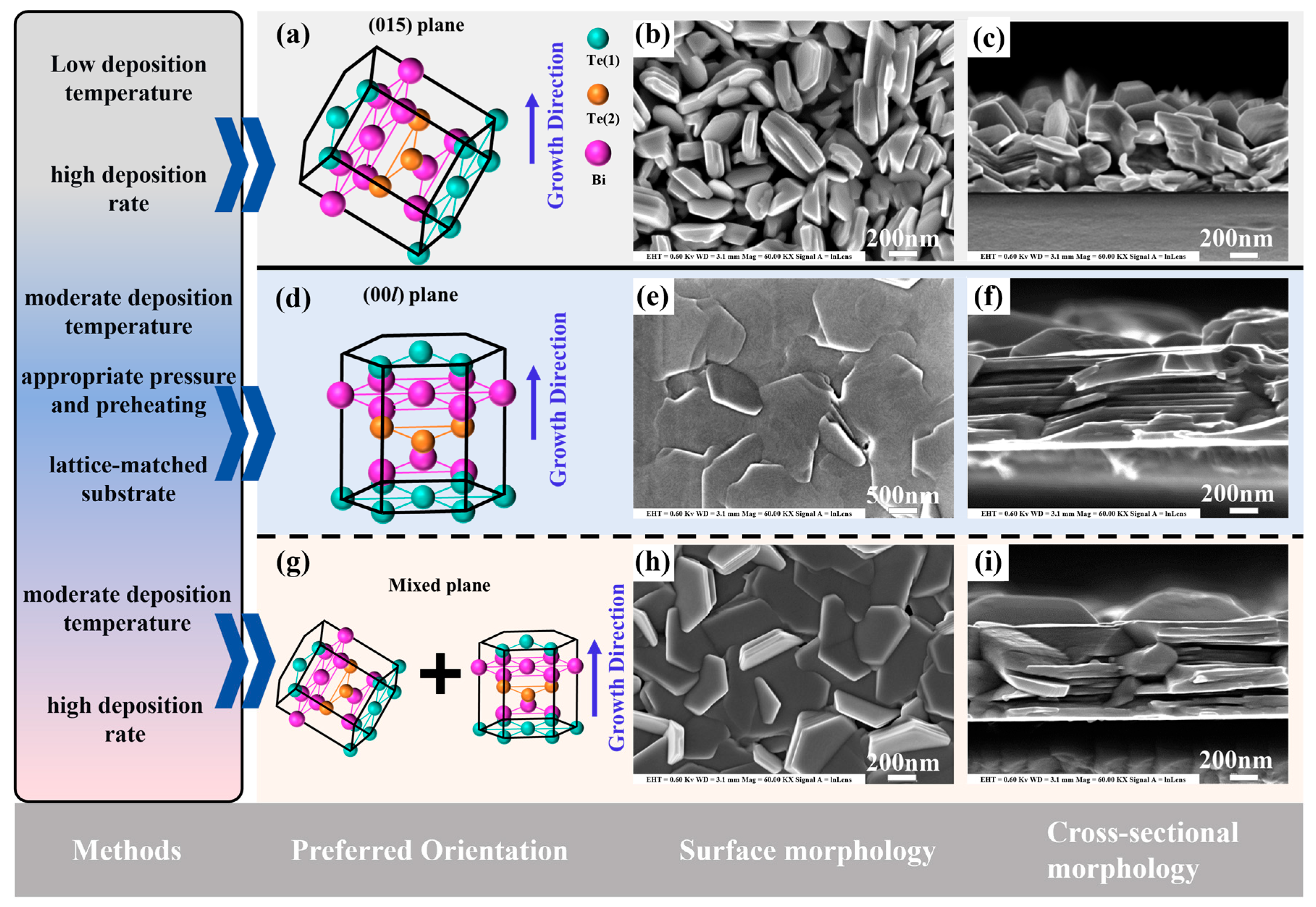
During the preparation of bismuth telluride (Bi2Te3)-based thin films by magnetron sputtering, an island-like morphology is primarily observed under conditions of limited surface atomic diffusion, such as low deposition temperatures or high deposition rates. Under these conditions, the film preferentially nucleates in the form of discrete nuclei and subsequently undergoes island growth and coalescence. Tao et al. directly observed this evolutionary pathway through AFM/SEM characterization of Bi2Te3/PET room-temperature DC magnetron-sputtered thin films: small islands formed at the initial stage increased in height and came into contact with one another as the film thickness increased, eventually coalescing into larger grains [41]. This process is accompanied by a dynamic evolution of surface roughness, providing direct evidence for the island growth mechanism under low-temperature sputtering conditions. While the pronounced (015) preferred orientation observed in XRD patterns is not directly equivalent to island growth, both the (015) texture and the granular morphology reflect similar non-equilibrium kinetic conditions. In terms of thermoelectric performance, phonons undergo intense scattering at the numerous nanostructured interfaces created during island-like film evolution, which significantly hampers their propagation. Through the strategic restriction of the phonon mean free path, the lattice-governed heat transport is effectively driven beneath its intrinsic bulk threshold. Concurrently, the potential barriers established at grain boundaries exert an ‘energy filtering’ influence; by obstructing the transport of cold carriers, these barriers elevate the mean energy of the remaining charge population, leading to a marked boost in the film’s Seebeck coefficient. The study by Chen et al. confirmed that this (015)-textured structure exhibits excellent power factor potential even in the early, non-continuous stage of film formation [40]. Furthermore, as shown in Figure 2a–c, the granular microstructure resulting from island growth can effectively relax internal stresses caused by thermal expansion mismatch or bending, thereby improving the adhesion and cyclic bending lifetime of the thin film on flexible substrates.

2.3.2. Lamellar Morphology (00l Preferred Orientation)

Throughout the synthesis of Bi2Te3-based films employing magnetron sputtering techniques, the formation of layered growth essentially depends on whether the in-plane migration ability of atoms after arriving at the substrate surface is sufficient to support preferential rearrangement along the basal plane. Bi2Te3 itself is stacked along the c-axis in quintuple layers, with the cleavage plane perpendicular to the c-axis. When (00l) diffraction peaks dominate the XRD pattern, it indicates that the c-axis of the film is essentially perpendicular to the substrate, as illustrated in Figure 2d–f, a horizontal alignment of the layered planes relative to the substrate is observed. This observation serves as a clear diffraction evidence for a strongly lamellar (00l) texture. Furthermore, the transport of heat and charge within the (00l) basal planes of Bi2Te3 is markedly superior to that occurring across the c-axis; therefore, (00l) texture is generally regarded as an important structural signature of layered preferential growth [42].
From the perspective of process parameters, the substrate temperature primarily determines the surface diffusion capability. Kim et al. found in co-sputtered Bi2Te3 thin films that as the deposition temperature increased, clear hexagonal grains appeared on the film surface above 290 °C, indicating that higher atomic mobility favors crystal rearrangement along low-surface-energy orientations [43]. However, excessively high temperatures can cause compositional deviation and induce phase transitions. Thus, the effect of temperature on layered growth exhibits a dual nature: promoting rearrangement at moderate temperatures and causing instability at excessive temperatures. The working pressure influences the layered orientation by controlling the collisional scattering of particles in Ar and their kinetic energy upon reaching the substrate. Nakano et al. pointed out that Higher argon pressure leads to a wider initial track width in the magnetron sputtering configuration, thereby affecting particle scattering and the sputtering rate [44]. Kianwimol et al. further showed that under appropriate pressure conditions combined with substrate pre-heating, flexible Bi2Te3 thin films can simultaneously achieve near-stoichiometric composition and strong (00l) orientation [45]. Their work explicitly identified the formation of (00l) orientation and subsequent diffusion as the key to obtaining this texture. The sputtering power/deposition rate indirectly affects the layered growth window by modifying the particle flux arriving at the substrate, surface residence time, and the resulting composition and grain size. The substrate type is also important. Shang et al. obtained clearly (00l)-textured Bi2Te3 thin layers synthesized via co-sputtering on single-crystal MgO substrates maintained at 400 °C, demonstrating that substrates with a template effect or better interfacial matching more readily induce layered preferential alignment [46].

2.3.3. Mixed Granular-Lamellar Morphology

During the preparation of bismuth telluride-based thin films by magnetron sputtering, a mixed granular-lamellar morphology is sometimes observed, which superficially resembles a Stranski-Krastanov (SK)-type “layer-then-island” process, though it is more accurately regarded as a mixed texture without direct in situ evidence of the nucleation pathway. As shown in Figure 2g–i: in this mode, a continuous or semi-continuous wetting layer initially forms on the substrate. Subsequently, due to interfacial energy, strain accumulation, and a renewed imbalance between surface diffusion and deposition flux, three-dimensional island-like grains nucleate and continue to grow. Zhu et al. observed a texture transformation in Bi0.5Sb1.5Te3 thin films deposited by DC magnetron sputtering [47], which they discussed in the context of the SK model; this transformation is essentially a thermally driven recrystallization of the as-deposited (015) texture into a (00l) texture. The minimization of cumulative interfacial energy acts as the primary catalyst for this structural evolution, reflecting a fundamental thermodynamic equilibrium process, the intensification of the layered texture is primarily driven by the in-plane transport and impingement of adatoms during the growth process. From the perspective of process parameters, the substrate temperature primarily determines the direction of this “layer vs. island” competition. When the temperature is too low, surface atomic migration is insufficient, and the growth approaches pure island nucleation. The working pressure influences the balance between “initial spreading” and “island stacking” by modulating the collisional scattering of sputtered particles in the Ar atmosphere and their kinetic energy upon reaching the substrate. Under appropriate working pressure combined with substrate pre-heating, nearly stoichiometric and highly (00l)-oriented Bi2Te3 thin layers can be successfully synthesized. The underlying mechanism is related to the formation of the (00l) orientation and subsequent diffusion processes.

3. Effects of Process Parameters, Post-Treatment, and Doping Modification on the Structure and Properties of Bi2Te3 Thin Films

During the highly non-equilibrium kinetic deposition process of magnetron sputtering, entropy (S) is not merely a passive physical parameter, but a critical factor determining the final microstructure, composition, and orientation of the thin films. By minimizing the system’s Gibbs free energy (G = HTS, where H is enthalpy, T is absolute temperature, and S is entropy), entropy exerts a decisive influence on the ultimate physical morphology of Bi2Te3 thin films across three core dimensions:
First, although high sputtering rates can trap atoms in kinetic minimums, resulting in rough polycrystalline or amorphous states, an entropy increase—given sufficient thermal activation—drives surface adatoms to overcome kinetic migration barriers and rearrange into a (00l)-oriented layered structure characterized by the lowest surface free energy. The work of Tang et al.explicitly points out that, under stable growth kinetics and sufficient thermodynamic (entropic) driving forces, the films can overcome random stacking and exhibit a highly ordered, layer-by-layer growth mode [48]. This demonstrates that entropy significantly influences the driving forces governing the morphological and orientational evolution of magnetron-sputtered Bi2Te3 films.
Second, the existence of configurational entropy dictates that an absolutely perfect crystal lattice is unstable at finite temperatures. To maximize configurational entropy and thereby lower the overall free energy, the spontaneous formation of a certain concentration of tellurium vacancies (VTe) and antisite defects (BiTe or TeBi) within the Bi2Te3 lattice is a thermodynamic inevitability. As confirmed by A. Hashibon et al. through first-principles density functional theory (DFT) calculations, such intrinsic point defects possess extremely low formation energies in Bi2Te3 [49]. The compensation effect of configurational entropy allows these defects to form abundantly at room temperature and typical deposition temperatures, thereby directly locking in the semiconductor type and electrical characteristics of the films during the initial deposition stages.
Finally, entropy is also a decisive factor in phase transitions and compositional deviations, as the high-entropy nature of the gas phase governs the phase stability of the films upon heating. Experiments conducted by K. Singkaselit et al. demonstrate that when the annealing temperature reaches 350 °C and above, the immense “vaporization entropy increase”—induced by Te atoms escaping the solid-state lattice into the gas phase—not only reduces the internal film density and increases surface roughness, but also directly triggers an irreversible structural collapse [50]. This ultimately drives the phase transition from Bi2Te3 to a Bi-rich BiTe structure.

3.1. Influence of Sputtering Process Parameters

During the preparation of Bi2Te3-based thin films by magnetron sputtering, the selection of deposition parameters directly determines the microstructure, stoichiometry, and ultimately the thermoelectric properties of the films. By precisely tuning the energy distribution and mass transport throughout the magnetron-based plasma deposition cycle, effective control over the quality of thin film growth can be achieved.

3.1.1. Sputtering Power and Deposition Rate

Sputtering power is a core physical parameter that controls the deposition rate, while the initial kinetic energy of adatoms is primarily governed by the target voltage (i.e., the discharge voltage), which is coupled to the sputtering power under typical operating conditions. Increasing the sputtering power significantly enhances the intensity of ion bombardment on the target surface and raises the instantaneous flux of ejected particles, thereby promoting grain growth while improving the deposition efficiency. Studies have shown that higher sputtering power endows the deposited atoms with greater initial kinetic energy. Particularly in DC magnetron sputtering, the direct transfer of kinetic energy results in significantly higher surface mobility of adatoms compared to RF sputtering at the same power level. This increased mobility facilitates the diffusion of atoms across the surface, allowing them to settle into the lowest-energy crystallographic positions, thereby improving film density, adhesion, and c-axis preferred orientation. However, excessively high deposition rates often lead to a kinetic locking effect, where atoms are buried by subsequent particles before they can complete long-range diffusion to lattice sites. This introduces a high density of point defects or dislocations and suppresses the preferential growth of (00l) planes. The systematic optimization study by Musri et al. confirmed that for Bi2Te3 thin films, 75 W is the optimal thereby identifying an optimal sputtering power that balances high crystalline quality, electrical conductivity, and the Seebeck coefficient; further increasing this power degrades the performance [51]. In practical processing, the power is typically maintained between 30 W and 75 W to achieve the best trade-off between deposition rate and thermoelectric performance.

3.1.2. Working Pressure and Particle Transport

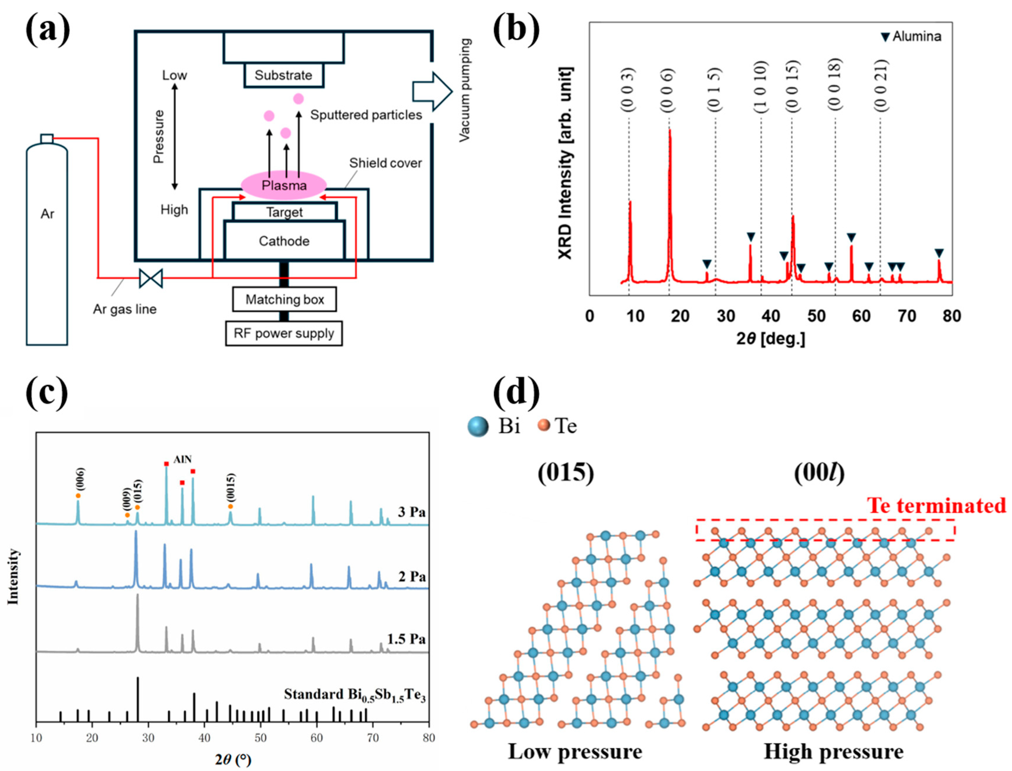
Working pressure is a key physical parameter that regulates the nucleation kinetics and composition transfer of Bi2Te3 thin films by adjusting the mean free path (MFP) and collision frequency of sputtered particles. At relatively low working pressures, the MFP of sputtered particles is long, and the frequency of collisional scattering among particles is extremely low, allowing most of the initial kinetic energy to be retained until the particles reach the substrate. The impact of such high-energy particles facilitates “congruent transfer” of the target composition and promotes the migration of adatoms on the substrate surface, leading to the formation of flat island structures with a high aspect ratio. Takashiri et al. developed a pressure gradient sputtering (PGS) system (as shown in Figure 3a) and, by exploiting the long MFP characteristics in the low-pressure region between the target and the substrate, successfully fabricated nanocrystalline thin films with an ultrahigh orientation factor [52]. Figure 3b presents the XRD parameters for the thin films that were derived via the following formula [28]:
F X = ( P P 0 ) / ( 1 P 0 )
P = I ( X ) / I h k l
P 0 = I 0 X / I 0 ( h k l )
where I(X), I0(X), I(hkl), and I0(hkl) represent the total integrated intensities of the X diffraction peak and P and P0 denote the integrated intensity ratios of the (hkl) peaks for the oriented and non-oriented samples; and F is the orientation factor, reaching a near-perfect value of 0.97. This study demonstrated that the PGS technique can effectively reduce plasma damage while significantly improving the crystalline maintaining thin-film quality even at high deposition rates.
As the working pressure increases, frequent collisions among particles lead to a decay in their average kinetic energy, producing a pronounced “thermalization” effect. However, a high-pressure environment can act as a critical leverage for decoupling transport properties, thereby bolstering the thermoelectric output within defined processing windows. It was revealed in the investigation conducted by Qu et al. that a relatively high deposition pressure (e.g., 3 Pa) effectively suppresses the re-evaporation of tellurium (Te), a volatile element, under thermally activated conditions, thereby maintaining the stoichiometric balance of the system and inducing the formation of a Te-rich (00l) surface (Figure 3c) [53]. As shown in Figure 3d, this structural transformation not only shifts the dominant crystallographic orientation from (015) to the thermodynamically more stable (00l) direction but also greatly enhances the carrier mobility μ by reducing the misorientation angle between grains and the interface barrier ɸb. Based on this regulation strategy, a remarkable peak ZT of 1.49 was recorded for the Bi0.5Sb1.5Te3 ternary layers at a near-ambient temperature of 313 K, demonstrating the central role of pressure control in optimizing carrier transport efficiency. Furthermore, the working pressure can sensitively tune the microstructure of the thin films by modulating the energy distribution of deposited atoms upon arrival at the substrate.

3.1.3. Substrate Temperature and Crystal Growth

Substrate temperature (Tsub) is a core variable that governs the transition of Bi2Te3-based thin films from non-equilibrium kinetically controlled growth to thermodynamically equilibrium growth. At low temperatures (below 200 °C), the thermal diffusion capability of adatoms is limited, and their surface diffusion distance remains significantly shorter than the mean spacing between adjacent nuclei. As a result, the film develops a granular, three-dimensional island-like morphology, often accompanied by a high density of point defects and disordered orientations. The kinetic agility of atoms across the substrate surface undergoes a substantial escalation in response to increased thermal input. According to first-principles calculations, the (00l) plane of Bi2Te3 possesses the lowest surface energy (0.16 J m−2), much lower than that of the (015) plane (0.37 J m−2). Therefore, a high-temperature environment drives atoms to migrate toward the lower-energy (00l) sites, promoting the development of a layered structure with a strong c-axis preferred orientation.
Adjusting the thermal pre-treatment from a baseline of 150 °C up to 350 °C yields a dramatic amplification in the film’s charge mobility (from 3.17 to 13.04 cm2 V−1 s−1), as documented by Sakulkalavek et al., the electrical conductivity increased nearly fivefold, and the power factor was also greatly enhanced [36]. Furthermore, Zhu et al. optimized the point defect chemistry within the film through a pronounced “in situ annealing” effect, resulting in denser columnar grains originating from the substrate [54]. The work by Chen et al. further indicated that when Tsub reaches 450 °C, cross-sectional profiling reveals a pronounced lamellar nanostructure immediately adjacent to the substrate, a structural signature typical of Frank-van der Merwe growth dynamics, whereas at Tsub = 350 °C, the cross-section exhibits an island-like nanostructure. Consequently, the thermal energy imparted by the substrate acts as the primary thermodynamic driver dictating the crystallographic texture during the onset of film growth.
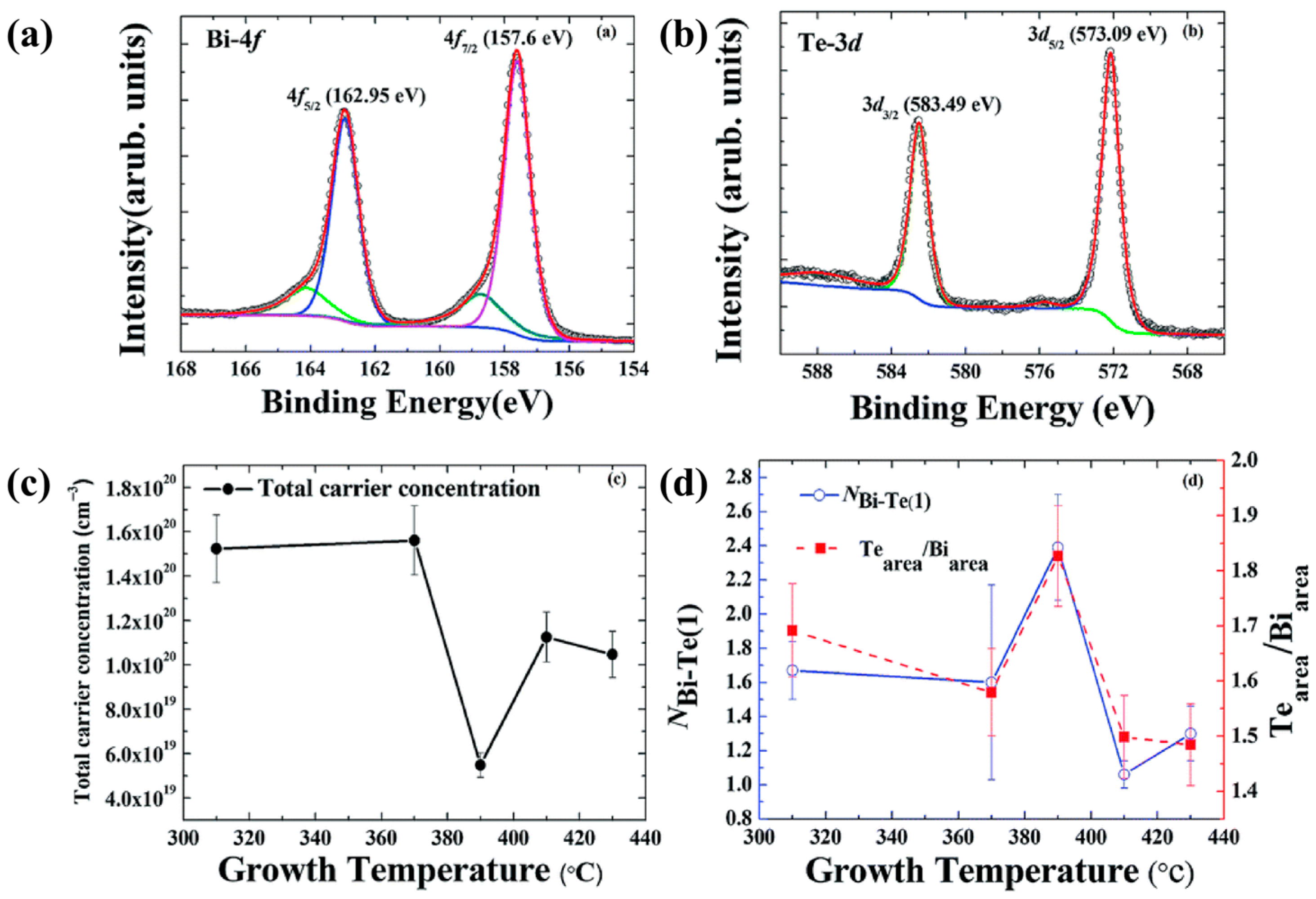
However, the substrate heating temperature itself significantly affects the Bi-to-Te atomic ratio during the sputtering process. Chuang et al. performed XPS measurements on Bi2Te3 thin films grown at different substrate temperatures [55]. Figure 4a,b show the Bi 4f and Te 3d core-level spectra of a representative film grown at 390 °C. The Te/Bi atomic ratio was calculated using the integrated peak areas. As shown in Figure 4d, as the growth temperature increases from 310 °C to 390 °C, the Te/Bi ratio gradually increases, reaching a maximum at 390 °C. This behavior indicates that within this temperature range, Te atoms progressively diffuse toward the outermost surface. When the growth temperature further rises above 390 °C, the Te/Bi ratio decreases monotonically, which can be attributed to enhanced thermal desorption of Te from the surface. The Te-rich condition at 390 °C corresponds to the minimum electron carrier concentration obtained from Hall measurements (Figure 4c), suggesting that under this growth condition, the concentration of acceptor-like BiTe antisite defects is maximized, partially compensating the electrons donated by donors (likely Te vacancies). Above 390 °C, the loss of Te suppresses the formation of BiTe and may favor the generation of donor-type TeBi antisite defects, leading to a higher electron carrier concentration and a downward shift in the Dirac point relative to the Fermi level. Therefore, XPS provides critical evidence that the growth-temperature-dependent stoichiometry directly influences the antisite defect equilibrium, which in turn tunes the electronic structure of Bi2Te3 thin films.

3.1.4. Target Composition and Thin Film Stoichiometry

Due to significant differences in the thermophysical properties of tellurium (Te) and bismuth (Bi), the thin film can easily deviate from the ideal stoichiometric ratio of 2:3 during deposition. The primary cause is the difference in their saturated vapor pressures. Investigations conducted by Xu and co-workers revealed that near 1042 K, the vapor pressure of Te is ~10 kPa, while that of Bi is only about 10 Pa [56]. This order-of-magnitude difference makes Te highly prone to re-evaporation during sputtering bombardment and nucleation, so that single-target sputtering typically produces non-stoichiometric thin films with Te deficiency [57]. To precisely compensate for Te loss, the study by Takashiri et al. demonstrated that using a Te-rich target with a special composition (e.g., 28 at.% Bi and 72 at.% Te) is an effective route to bring the film composition toward equilibrium [52]. Furthermore, dual-target simultaneous sputtering from a compound Bi2Te3 target and a pure tellurium target and a Te target allows for independent adjustment of the power for each target, enabling precise control over the Bi:Te atomic ratio over a wide range from 1.9 to 3.2.
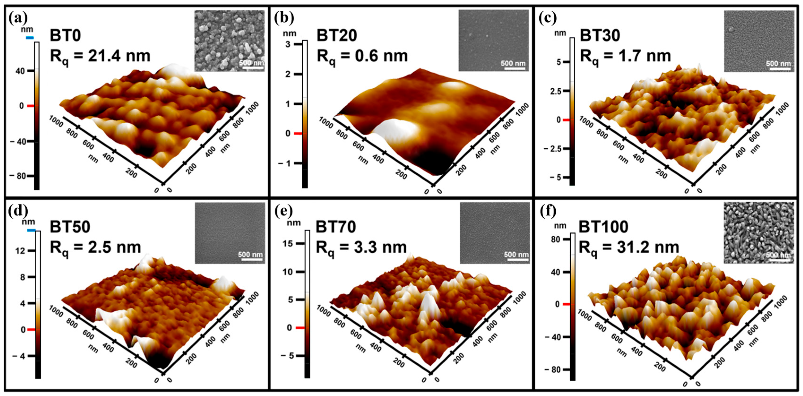
Following a similar co-sputtering approach with pure elemental targets, Mun et al. effectively controlled the final chemical composition of the deposited films by systematically adjusting the radio frequency (RF) sputtering powers of the bismuth (Bi) target (5–15 W) and the tellurium (Te) target (10–30 W). Fabricating a series of bismuth telluride thin films with varying Te atomic percentages (designated as BT0 to BT100, where the numbers represent the relative atomic percentage of Te) [58]. As illustrated in Figure 5a–f, atomic force microscopy (AFM) characterizations demonstrated that the pristine Bi thin film (BT0) and pristine Te thin film (BT100) exhibited extremely high root-mean-square roughness (Rq) values of 21.4 nm and 31.2 nm, respectively, owing to their large grain sizes. In stark contrast to the pristine thin films, the intermediate-composition thin films (BT20 to BT70) displayed relatively smooth surfaces with no distinct isolated grains observed under the microscope, resulting in substantially reduced Rq values.
The compositional deviation of the film directly determines its thermoelectric transport characteristics and carrier polarity through the regulation of intrinsic point defect types. Studies have shown that in a Te-rich environment, excess Te atoms tend to occupy Bi sites, forming TeBi anti-site defects, which act as donors and induce n-type conduction in the film [59]. In contrast, a Te-deficient (Bi-rich) environment promotes Bi atoms to occupy Te sites, forming BiTe anti-site defects, which produce an acceptor effect and result in p-type characteristics. The experiments by Musri et al. further confirmed that even slight compositional deviations significantly shift the Fermi level position, and excessive deviation from stoichiometry leads to lattice constant contraction and reduced crystallinity, thereby impairing carrier mobility [51]. Therefore, in magnetron sputtering processes, maintaining the Bi:Te atomic ratio slightly above 1.5 through target composition design or co-sputtering compensation is an essential condition for curbing intrinsic anti-site defects while concurrently elevating the electrical power factor [60].
The surface energy, lattice matching, and structural symmetry of the substrate are key factors determining the quality of van der Waals epitaxy (vdW Epitaxy) of Bi2Te3. Substrates can be broadly classified into two categories: rigid and flexible. On rigid single-crystal substrates with hexagonal symmetry (e.g., MgO or Si (111)), Bi2Te3 tends to grow with a preferred orientation along the c-axis. Because such substrates provide a good geometric template, the films typically exhibit a clear step-terrace flow growth mode and form flat atomic terraces with large grains, which is crucial for reducing carrier scattering [61]. Flexible polymer substrates are mainly used in wearable thermoelectric applications; poly(ethylene terephthalate) (PET) and polyimide (PI) have emerged as a focal point of recent research, primarily owing to their exceptional mechanical resilience. A pronounced thermomechanical incompatibility exists at the interface, driven by the stark disparity in thermal expansivities between the deposited layer and the non-crystalline base. Data comparison: the CTE of Bi2Te3 is ~20 × 10−6 K−1, while that of a typical PI substrate is only 12 × 10−6 K−1. However, according to the interfacial strain regulation mechanism, despite the physical mismatch, studies have found that by controlling the process to induce a specific island-like growth structure in the film, a microscopic “stress buffer zone” can be created. This structure effectively decouples mechanical strain during macroscopic bending, prevents the formation of through-thickness cracks in the continuous film, and thus significantly improves the adhesion and cyclic fatigue life of flexible devices [62].

3.2. Regulation of Microstructure and Properties by Annealing Treatment

3.2.1. Effect of Annealing Temperature on Grain Growth and Defect Elimination

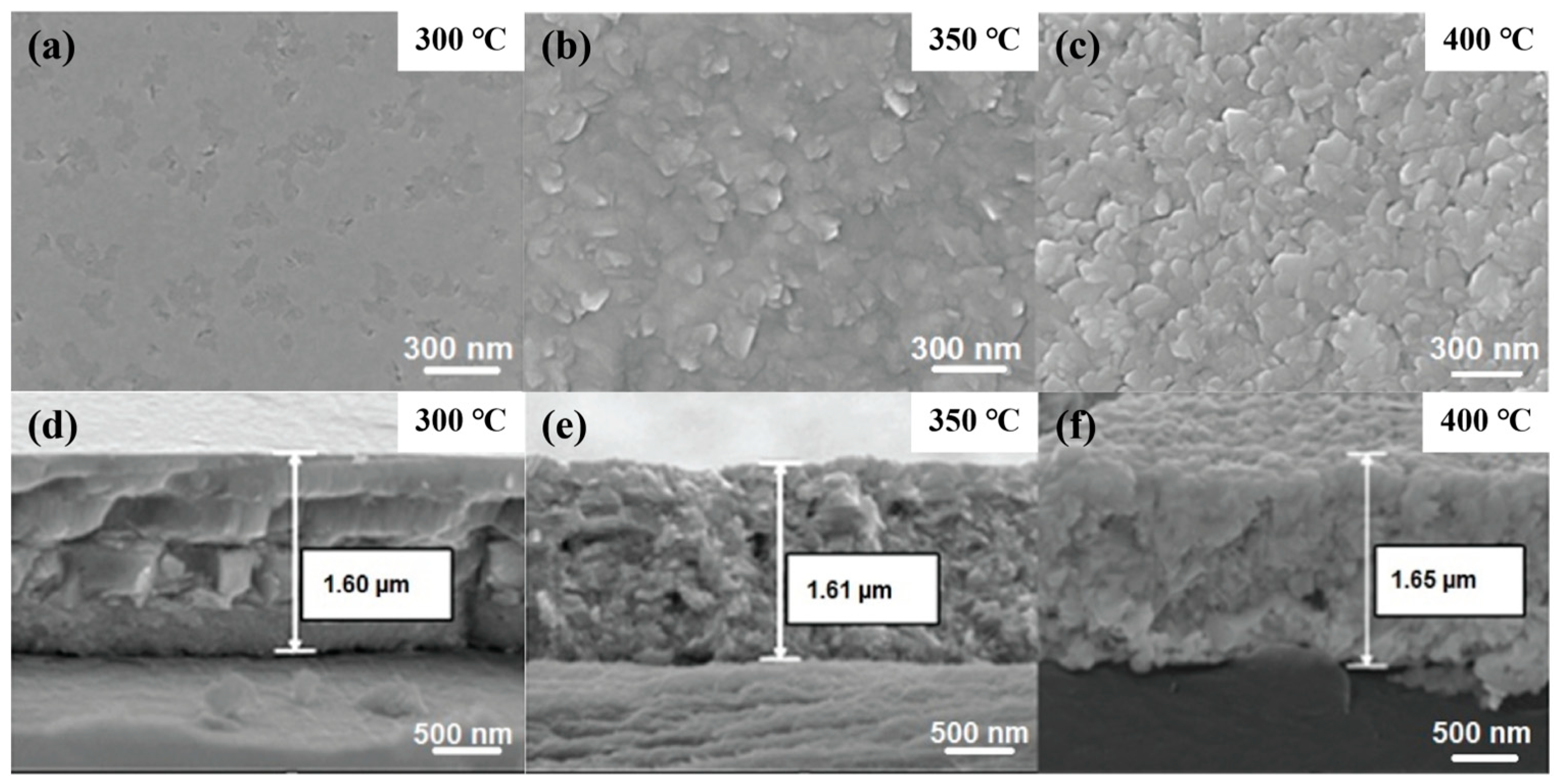
Annealing is a critical post-treatment process for optimizing the thermoelectric performance of bismuth telluride (Bi2Te3) thin films. Its core function lies in modulating the crystallinity, microstructure, and intrinsic point defect concentration of the films. The study by Singkaselit et al. demonstrates that the annealing temperature directly determines the structural evolution pathway and the final electrical transport properties of the films [50]. In the lower temperature range (e.g., 300 °C), annealing effectively promotes atomic migration and rearrangement, thereby significantly enhancing the crystallinity and increasing the grain size. This grain growth process reduces the number of grain boundaries within the film, thereby weakening carrier scattering at grain boundaries and consequently enhancing the macroscopic carrier mobility. As shown in Figure 6a,d, appropriate thermal treatment helps eliminate residual stress generated during film deposition, resulting in a smoother surface and a denser internal structure. However, when the annealing temperature rises to 350 °C or higher, the defect evolution mechanism of the Bi2Te3 film changes markedly.
Owing to the high saturated vapor pressure of tellurium (Te), the elevated temperature intensifies the volatilization of Te atoms, generating a large number of Te vacancies (VTe) within the film. These defect reactions driven by Te loss not only alter the carrier concentration but can also induce irreversible phase transformation at extremely high temperatures (e.g., above 350 °C), converting the original Bi2Te3 structure into a Bi-rich BiTe structure. As illustrated in Figure 6b,c,e,f, this phase transformation is accompanied by a decrease in internal density and a deterioration in mechanical hardness, as well as a surge in the free carrier concentration, leading to a reduction in the Seebeck coefficient. Zheng et al. deposited n-type Bi2Te3 thin films. As the annealing temperature increased from 100 °C to 400 °C, grain growth along the c-axis direction and crystallinity were significantly enhanced, and an optimal power factor of 1.10 × 10⁻³ W m−1 K−2 was obtained at 300 °C [63]. Raising the annealing temperature from 100 °C to 300 °C led to higher XRD peak intensities, which suggests grain growth and enhanced crystalline quality following the annealing process. However, when the temperature was raised to 400 °C, the intensity of the (015) peak decreased. Thus, overly high annealing temperatures can cause the evaporation of select elements and boost oxygen traces, which consequently raises defect levels and aggravates thermal stress. Therefore, precise control of the annealing temperature is crucial for balancing grain boundary scattering, defect concentration, and phase stability in the thin films.

3.2.2. Effect of Annealing Time on Grain Growth and Defect Elimination

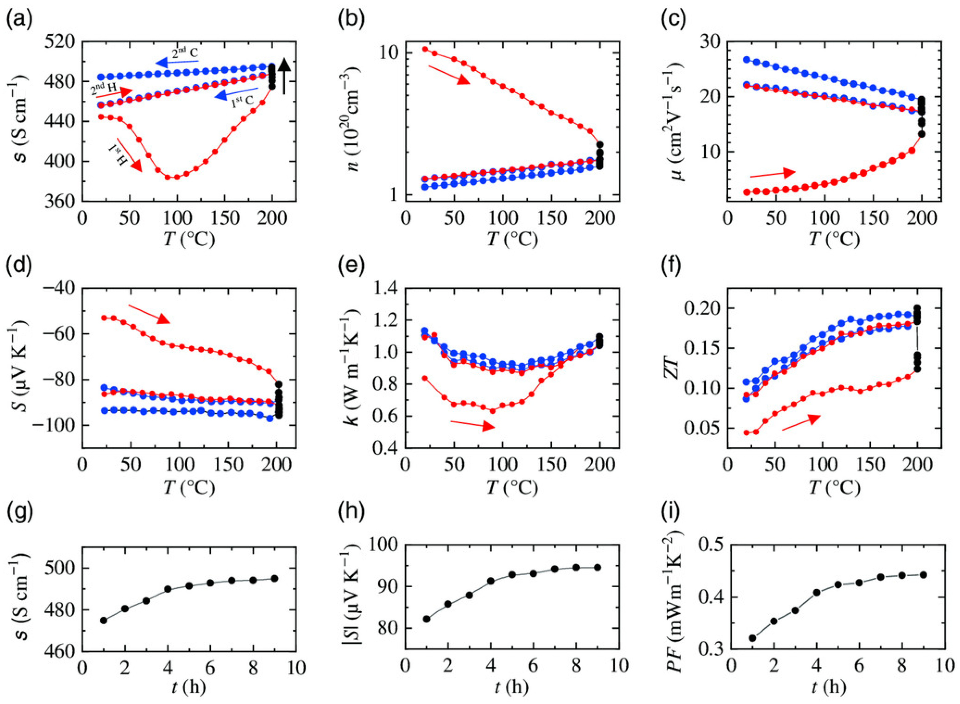
In contrast to annealing temperature, there have been relatively few systematic investigations into how annealing time affects grain growth in Bi2Te3 are relatively scarce. Nevertheless, some studies have demonstrated that annealing time is also an important factor influencing grain growth of Bi2Te3. He et al. prepared n-type Bi2Te3-based thin films by DC magnetron sputtering at 300 °C and systematically investigated the effect of in situ annealing time on the thermoelectric properties of the films. The results showed that increasing the sputtering power led to a higher deposition rate and larger grain size. After determining the optimal sputtering power of 30 W, the performance was further optimized through an in situ annealing process. The results indicated that the film annealed for 40 min exhibited a significant decrease in electrical conductivity due to a reduction in carrier concentration, while the Seebeck coefficient was enhanced. A maximum power factor of 0.82 mW m−1 K−2 was obtained at 543 K [54]. This finding suggests that an appropriate annealing time is crucial for balancing carrier concentration and the Seebeck coefficient, thereby optimizing thermoelectric performance. Naumochkin et al. systematically studied the impact of annealing on sputtered Bi2Te3 thin films, focusing on the roles of annealing duration and temperature in 90 nm-thick samples. Experiments illustrated in Figure 7a–i show that film thickness and optimal annealing time are linked—namely, thicker films demand extended annealing durations to attain peak ZT and power factor [64]. This finding reveals a coupling effect between annealing time and material scale, providing valuable guidance for the design of annealing processes for films of different thicknesses in practical applications.

3.2.3. Role of Annealing Atmosphere (Vacuum, Inert, Reducing)

The effects of annealing temperature and time on grain growth and defect elimination in Bi2Te3 have been systematically discussed above. However, the microstructure and thermoelectric behavior of Bi2Te3 are also strongly influenced by the annealing atmosphere. Since Bi2Te3 contains the volatile element Te, the annealing atmosphere directly affects the volatilization behavior of elements, defect evolution, and phase stability, consequently setting the materials’ electrical and thermal conduction behavior. According to the mechanisms of different atmospheres, three types of annealing can be classified: vacuum annealing, inert atmosphere annealing, and reducing atmosphere annealing.
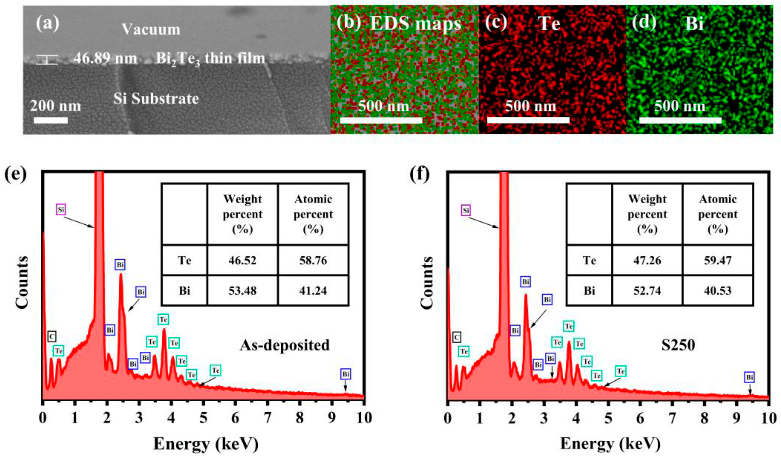
Scanning electron microscopy (SEM) was employed to characterize the cross-sectional morphology of the thin films after annealing. As illustrated in Figure 8a, the film thickness of the S250 sample (annealed at 250 °C) is estimated to be ~47 nm, where the vacuum environment, Bi2Te3 layer, and Si substrate are clearly distinguished, demonstrating excellent film formation. Vacuum annealing is a critical heat treatment method for Bi2Te3 materials, as its core function is to regulate the elemental stoichiometry and structural evolution of the films. Zhang et al. systematically investigated the compositional optimization and defect elimination of sputtered Bi2Te3 thin films during vacuum thermal processing [65]. As shown in the EDS mapping of Figure 8b–d, the Bi and Te elements are uniformly and continuously distributed across the substrate after annealing, indicating high film quality without noticeable elemental segregation. Figure 8e,f reveal that for the as-deposited specimen, the atomic ratio of Bi to Te is ~0.70, representing a notable deviation from the ideal stoichiometry; this indicates that the initial deposition process introduces a certain degree of elemental disorder. A clear correlation exists between vacuum annealing and compositional stabilization. Specifically, after annealing at 250 °C, the atomic ratio of Bi to Te decreases to 0.68, which is significantly closer to the standard stoichiometric ratio of 0.67 for Bi2Te3. The effective thermal activation promotes atomic rearrangement from a disordered amorphous state into a highly ordered crystalline structure. This microstructural evolution significantly reduces internal defects such as grain boundaries, vacancies, and interstitial atoms, thereby fundamentally enhancing the physical and thermoelectric properties of the sample. This research demonstrates that appropriate vacuum annealing effectively minimizes stoichiometric deviations and structural defects, revealing the underlying mechanism of composition homogenization and quality improvement during thermal treatment.
Inert atmosphere annealing (e.g., Ar or N2 atmosphere) primarily optimizes thermoelectric performance by suppressing oxidation and regulating the microstructure. Compared to vacuum annealing, an inert atmosphere can inhibit excessive volatilization of Te to a certain extent while providing a relatively stable thermal environment. Wang et al. used N2 as a shielding gas during annealing and obtained a stable Bi2Te3/W multilayer structure. The multilayer structure of Bi2Te3/W thin films can reasonably regulate the carrier concentration and filter low-energy carriers, thereby simultaneously enhancing the electrical conductivity and Seebeck coefficient. The power factor of Bi2Te3/W reaches 1785 μW m−1 K−2 at 600 K [66]. Compared to vacuum annealing, which is prone to severe Te volatilization, and inert gas annealing, which only passively prevents oxidation, reducing atmosphere annealing (such as a hydrogen-argon mixture) can actively and chemically reduce the insulating oxides (e.g., Bi2O3 and TeO2) on the film surfaces and grain boundaries into pure metallic elements. This process deeply purifies the grain boundaries and interfacial defects of the material without causing severe stoichiometric deviations. Consequently, reducing atmosphere annealing substantially weakens the interfacial scattering of charge carriers caused by insulating barriers, thereby significantly enhancing the carrier mobility, electrical conductivity, and the overall power factor of bismuth telluride thin films [67].

3.2.4. Comparison Between Rapid Thermal Annealing and Conventional Tube Furnace Annealing

The core difference between different annealing methods lies in the temperature and time history of the heat treatment, which directly determines the evolution path of the material’s microstructure. Specifically, conventional tube furnace annealing (TFA) typically employs a slow heating rate (5–10 °C min−1) and a long holding time (several hours or even tens of hours), relying on thermal radiation and convection heating [65,68]. In contrast, rapid thermal annealing (RTA) uses radiative heating sources such as lasers, allowing the heat treatment process to be completed within seconds to minutes. The production rate of Bi2Te3 was around 180 times higher than that of conventional thermal annealing, thereby significantly shortening the process cycle [69]. From an equipment perspective, rapid thermal annealing furnaces differ significantly from conventional tube furnaces in terms of heating method, heating efficiency, temperature range, and structural design.
In recent years, rapid thermal annealing has achieved notable progress in the research of Bi2Te3 thin-film thermoelectric materials, attracting widespread attention due to its short-duration, high-efficiency characteristics. Zheng et al. prepared Bi2Te3 nanocrystalline thin films on polymer substrates using a single-source evaporation method and applied rapid thermal treatment. The study found that rapid annealing effectively improved the crystallinity of the films and enabled control over grain size, yielding a pure Bi2Te3 phase with nanoscale grains and ultimately increasing the ZT value to 0.5 [70]. N-type and p-type Bi2Te3 thin films were fabricated by Rashid et al. via constant-current electrodeposition, followed by a systematic study of the RTA treatment’s impact on the microstructural and thermoelectric characteristics. The Seebeck coefficient of the n-type thin film increased from −57 μV K−1 to −169 μV K−1, and that of the p-type film increased from 28 μV K−1 to 112 μV K−1; the power factor was enhanced approximately sixfold for the n-type film and about twofold for the p-type film [71]. This research clearly shows that a short-duration rapid thermal treatment can greatly boost the thermoelectric properties of Bi2Te3, highlighting distinct advantages in terms of the process.
Conventional tube furnace annealing, as a standard method for material heat treatment, is also widely used in the research of Bi2Te3-based materials. Yamashita and Tomiyoshi reported that after vacuum annealing of p-type Bi2Te3 at 673 K for 2 h, the room-temperature power factor increased from 4.25 × 10⁻³ W m−1 K−2 to 5.72 × 10⁻³ W m−1 K−2, representing an improvement of ~35% [72]. However, conventional tube furnace annealing typically requires several hours or even longer processing times, resulting in a long process cycle and high energy consumption. Moreover, prolonged high-temperature heat treatment may induce volatilization loss of Te and compositional deviation.

3.3. Research Progress on Doping Modification

3.3.1. n-Type Doping

To achieve n-type doping, incorporating selenium to create Bi2Te3-xSex solid solutions proves effective for boosting thermoelectric performance. Bi2Te3 and Bi2Se3 share the same rhombohedral crystal structure, and they can form a continuous solid solution Bi2Te3-xSex over the entire composition range [73]. During the formation of the solid solution, Se atoms with higher electronegativity preferentially occupy Te lattice sites. Because selenium has a smaller atomic radius than tellurium, the lattice constant steadily decreases as the Se doping level rises. Meanwhile, the formation of Bi-Se bonds enhances the chemical bonding strength within the lattice, leading to a gradual increase in the band gap [74].
In Bi2Se3, the formation energies of the anti-site defects BiTe and TeBi are similar (~0.6 eV), allowing both to coexist at relatively high concentrations and thereby inducing a high density of diverse microstructures (e.g., ripple dislocations, edge dislocations, staggered bilayer structures, etc.). In contrast, in Bi2Se3, the formation energies of the anti-site defects BiSe and SeBi are relatively high (~1.3 eV), making it difficult for both to form simultaneously in large quantities, which results in a more regular atomic arrangement [75]. Consequently, when Se is incorporated into the Bi2Te3 lattice, the defect characteristics and microstructure of the system change, thereby affecting the mechanical properties and thermoelectric transport behavior. The results indicate that when the Se solid solution content is below 20%, Bi2(Te, Se)3 crystals still maintain good plastic deformability (maximum bending strain ≥ 10%) while simultaneously exhibiting high thermoelectric performance.
As the Se doping content increases, the carrier concentration of the system exhibits a decreasing trend, which is mainly attributed to the modulation of defect equilibrium and band structure by Se doping. The decrease in carrier concentration leads to a reduction in electrical conductivity on the one hand, but on the other hand significantly enhances the Seebeck coefficient, which is attributed to the effective increase in the density of states and the shift in the Fermi level toward the interior of the band gap. This research has shown that by optimizing the Se doping concentration, an optimal trade-off between electrical conductivity and the Seebeck coefficient can be achieved, thereby maximizing the power factor [76].

3.3.2. p-Type Doping

Unlike the Se substitution at Te sites in n-type Bi2Te3-xSex solid solutions, the p-type doping strategy mainly employs Sb substitution at Bi sites to form (Bi1-xSbx)2Te3 solid solutions. Sb and Bi belong to the same group of VA elements and possess similar chemical properties and electronic configurations; therefore, Sb substitution for Bi can effectively convert the conduction type from n-type to p-type while maintaining the integrity of the crystal structure [77,78]. Bi2Te3 crystallize in the rhombohedral structure (space group R3m) and can mix to form a continuous solid solution over a wide range of compositions. The atomic size of Sb (~1.59 Å) is marginally smaller than that of Bi (~1.63 Å). Consequently, higher Sb substitution levels lead to a monotonic drop in the lattice constant, analogous to the contraction effect caused by Se doping in n-type systems [75].
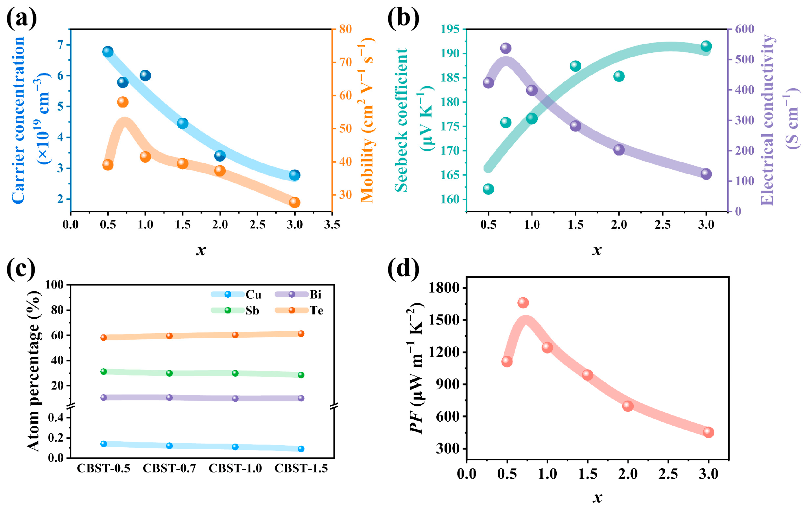
Building upon this fundamental (Bi,Sb)2Te3 (BST) solid solution framework, further doping modification and stoichiometric regulation serve as cornerstone strategies for fine-tuning carrier transport properties and suppressing the detrimental bipolar effect. Specifically, the incorporation of transition metal elements like copper (Cu) into the p-type BST system has demonstrated remarkable efficacy in performance optimization. Cu is particularly favored as an external dopant because its electronegativity and atomic radius are comparable to those of Sb. During the magnetron sputtering process, Cu atoms preferentially occupy Sb sites in the lattice, functioning as acceptor dopants that introduce additional holes into the system. This mechanism effectively elevates the hole carrier concentration and compensates for minority electron generation, thereby suppressing the intrinsic excitation that typically degrades thermoelectric performance at elevated temperatures. Research by Ge et al. shows that optimized Cu-doped films to exhibit an optimized carrier concentration of 5.78 × 1019 cm−3 and an enhanced mobility of 58.0 cm2 V−1 s−1 at room temperature, while achieving a peak Seebeck coefficient of 203 μV K−1 at 400 K due to the effective mitigation of the bipolar effect (Figure 9a,b) [79].
As shown in Figure 9c, beyond external element doping, “self-doping” via stoichiometric adjustment remains a critical regulatory dimension. The intrinsic carrier concentration in BST systems is primarily governed by the dynamic equilibrium between antisite defects (e.g., SbTe, BiTe) and tellurium vacancies (VTe). During sputtering, process parameters such as working pressure significantly influence the “re-sputtering” effect of weakly bonded Sb atoms, thereby shifting the Te/(Bi + Sb) ratio and altering the concentration of hole-generating antisite defects.
Recently, these synergistic approaches have challenged the traditional paradigm that high thermoelectric performance is exclusively tied to the (00l) preferential orientation. By coupling optimized Cu-acceptor doping with precise pressure-controlled defect and grain growth engineering, non-(00l) layered flexible p-type films (e.g., (015) oriented) have achieved a room-temperature power factor (PF) of 1660 μW m−1 K−2 (Figure 9d). This represents one of the highest reported values for non-(00l) oriented films, underscoring the potential of combining structural engineering with multi-element doping to develop high-efficiency, flexible thermoelectric devices. To provide a comprehensive comparison, the thermoelectric performance parameters of various doped bismuth telluride thin films are summarized in Table 1.

4. Conclusions and Outlook

Recent milestones achieved in the magnetron sputtering deposition of Bi2Te3-based layers are comprehensively outlined in this article, with an emphasis on the intrinsic relationships among process parameters, microstructures, and thermoelectric performance. Ultimately, the microstructural evolution and growth kinetics of the thin films are governed by a synergistic interplay of deposition variables—primarily discharge power, chamber pressure, substrate temperature, and source stoichiometry. These factors, along with the substrate type, critically determine the film growth mode (island, layered, or mixed), stoichiometry, defect chemistry, and preferred orientation, thereby dictating the resulting Seebeck coefficient, electrical conductivity, and thermal conductivity. Post-annealing treatments—including temperature, time, atmosphere (vacuum, inert, or reducing), and method (conventional tube furnace versus rapid thermal annealing)—effectively modulate grain size, crystallinity, point defects, and Te volatilization, effectively optimizing the trade-off between electrical and thermal transport, leading to a concomitant boost in both power factor and ZT value. Doping modification, particularly n-type Se doping and p-type Sb doping, adjusts the carrier concentration and band structure while also altering defect formation energies and microstructural features (e.g., dislocations and layered defects), offering additional degrees of freedom for optimizing both thermoelectric and mechanical properties. Despite these advances, several challenges remain. The lack of systematic comparability across studies due to widely varying deposition conditions hinders the establishment of general process—structure—property maps. Furthermore, the scalability of magnetron sputtering for industrial production of flexible thermoelectric devices requires better control over large-area uniformity, substrate compatibility, and long-term stability. Future research should focus on establishing high-throughput experimental or machine-learning-assisted frameworks to rapidly identify optimal sputtering conditions, exploring novel multilayer or superlattice architectures to further decouple electrical and thermal transport, developing in situ characterization techniques to monitor growth and annealing dynamics, and integrating Bi2Te3 thin films into functional microdevices (e.g., on-chip coolers and wearable sensors) with demonstrated reliability. Addressing these issues will accelerate the practical application of magnetron-sputtered Bi2Te3 thin films in next-generation energy harvesting and thermal management systems.

Author Contributions

Conceptualization, W.G. and P.Z.; Methodology, W.G. and P.Z.; Software, S.L.; Validation, W.G., S.L. and Y.D.; Investigation, W.G. and Y.D.; Writing—original draft preparation, W.G. and Y.D.; Writing—review and editing, W.G. and P.Z.; Visualization, W.G. and H.S.; Supervision, P.Z. and H.S.; Project administration, P.Z.; Funding acquisition, P.Z. All authors have read and agreed to the published version of the manuscript.

Funding

This research was funded by National Natural Science Foundation of China (No. U2230131), Key Science and Technology Project of Shenzhen (No. 202407005), A Project Funded by the Priority Academic Program Development of Jiangsu Higher Education Institutions, Jiangsu Collaborative Innovation Center for Advanced Inorganic Function Composites, Nanjing Tech University.

Data Availability Statement

No new data were created or analyzed in this study. Data sharing is not applicable to this article.

Conflicts of Interest

The authors declare no conflicts of interest.

References

  1. Witting, I.T.; Chasapis, T.C.; Ricci, F.; Peters, M.; Heinz, N.A.; Hautier, G.; Snyder, G.J. The Thermoelectric Properties of Bismuth Telluride. Adv. Electron. Mater. 2019, 5, 1800904. [Google Scholar] [CrossRef]
  2. Goldsmid, H.J.; Underwood, F.A. Study of Orientation in Polycrystalline Bismuth Telluride Alloys. Adv. Energy Convers. 1968, 7, 297–301. [Google Scholar] [CrossRef]
  3. Teweldebrhan, D.; Goyal, V.; Balandin, A.A. Exfoliation and Characterization of Bismuth Telluride Atomic Quintuples and Quasi-Two-Dimensional Crystals. Nano Lett. 2010, 10, 1209–1218. [Google Scholar] [CrossRef]
  4. Goldsmid, H.J. Bismuth Telluride and Its Alloys as Materials f or Thermoelectric Generation. Materials 2014, 7, 2577–2592. [Google Scholar] [CrossRef]
  5. Puneet, P.; Podila, R.; Karakaya, M.; Zhu, S.; He, J.; Tritt, T.M.; Dresselhaus, M.S.; Rao, A.M. Preferential Scattering by Interfacial Charged Defects for Enhanced Thermoelectric Performance in Few-Layered n-Type Bi2Te3. Sci. Rep. 2013, 3, 3212. [Google Scholar] [CrossRef]
  6. Guan, T.; Gao, J.; Hua, C.; Tao, Y.; Ma, Y.; Liu, J. Liquid Metal Enabled Thermoelectric Effects: Fundamental and Application. Adv. Funct. Mater. 2025, 35, 2423909. [Google Scholar] [CrossRef]
  7. Snyder, G.J.; Toberer, E.S. Complex Thermoelectric Materials. Nat. Mater. 2008, 7, 105–114. [Google Scholar] [CrossRef]
  8. Abinaya, R.; Harish, S.; Ponnusamy, S.; Shimomura, M.; Navaneethan, M.; Archana, J. Enhanced Thermoelectric Figure-of-Merit of MoS2/α-MoO3 Nanosheets via Tuning of Sulphur Vacancies. Chem. Eng. J. 2021, 416, 128484. [Google Scholar] [CrossRef]
  9. Zhang, Q.; Deng, K.; Wilkens, L.; Reith, H.; Nielsch, K. Micro-Thermoelectric Devices. Nat. Electron. 2022, 5, 333–347. [Google Scholar] [CrossRef]
  10. Sajid, M.; Hassan, I.; Rahman, A. An Overview of Cooling of Thermoelectric Devices. Renew. Sustain. Energy Rev. 2017, 78, 15–22. [Google Scholar] [CrossRef]
  11. Li, W.; Zhang, X.; Liu, H.; Shu, M.; Zhang, C.; Zong, P. Two-Dimensional van Der Waals Stack Heterostructures for Flexible Thermoelectrics. Nano Energy 2024, 125, 109605. [Google Scholar] [CrossRef]
  12. Shu, M.; He, Z.; Zhu, J.; Ji, Y.; Zhang, X.; Zhang, C.; Chen, M.; Zong, P. Flexible Thermoelectric BiSbTe/Carbon Paper/BiSbTe Sandwiches for Bimode Temperature-Pressure Sensors. Adv. Funct. Mater. 2024, 35, 2414660. [Google Scholar] [CrossRef]
  13. Wan, C.; Tian, R.; Azizi, A.B.; Huang, Y.; Wei, Q.; Sasai, R.; Wasusate, S.; Ishida, T.; Koumoto, K. Flexible Thermoelectric Foil for Wearable Energy Harvesting. Nano Energy 2016, 30, 840–845. [Google Scholar] [CrossRef]
  14. Ranganayakulu, V.K.; Wang, T.-H.; Chen, C.-L.; Huang, A.; Ma, M.-H.; Wu, C.-M.; Tsai, W.-H.; Hung, T.-L.; Ou, M.-N.; Jeng, H.-T.; et al. Ultrahigh zT from Strong Electron–Phonon Interactions and a Low-Dimensional Fermi Surface. Energy Environ. Sci. 2024, 17, 1904–1915. [Google Scholar] [CrossRef]
  15. Wong, W.P.; Elsa, G.; Mustafa, M.N.; Walvekar, R.; Numan, A.; Khalid, M.; Lau, P.L. Bismuth Telluride-Based Thermoelectric Generators: Advances in Synthesis, Performance Enhancement, and Device Applications. J. Power Sources 2025, 653, 237722. [Google Scholar] [CrossRef]
  16. Phan, T.T.T.; Nguyen, L.T.T.; Trieu, Q.T.; Le, N.V.; Ung, T.D.T.; Park, S.; Tran, V.C.; Phan, T.B.; Pham, A.T.T. Thickness-Controlled Decoupling of the Thermoelectric Trade-off in ZnO Thin Films via Density-of-States Effective Mass Modulation. Scr. Mater. 2026, 279, 117307. [Google Scholar] [CrossRef]
  17. Benjamin, S.L.; de Groot, C.H.; Gurnani, C.; Hector, A.L.; Huang, R.; Koukharenko, E.; Levason, W.; Reid, G. Controlling the Nanostructure of Bismuth Telluride by Selective Chemical Vapour Deposition from a Single Source Precursor. J. Mater. Chem. A 2014, 2, 4865–4869. [Google Scholar] [CrossRef]
  18. Zhu, J.; Sun, C.; Feng, W.; Chen, M.; Zong, P.-A.; Wan, C. Permeable Carbon Fiber Based Thermoelectric Film with Exceptional EMI Shielding Performance and Sensor Capabilities. J. Adv. Ceram. 2024, 13, 1119–1131. [Google Scholar] [CrossRef]
  19. Rodrigues-Junior, G.; Chagas, T.; Reis, R.; Sciammarella, P.V.; Fornari, C.I.; Rappl, P.H.O.; Abramof, E.; Magalhães-Paniago, R.; Malachias, Â. Local Surface Electronic Response of Bi2Te3 Topological Insulator upon Europium Doping. Phys. Rev. B 2023, 108, 035408. [Google Scholar] [CrossRef]
  20. Carter, M.J.; El-Desouky, A.; Andre, M.A.; Bardet, P.; LeBlanc, S. Pulsed Laser Melting of Bismuth Telluride Thermoelectric Materials. J. Manuf. Process. 2019, 43, 35–46. [Google Scholar] [CrossRef]
  21. Zhou, Y.; Li, L.; Tan, Q.; Li, J.-F. Thermoelectric Properties of Pb-Doped Bismuth Telluride Thin Films Deposited by Magnetron Sputtering. J. Alloys Compd. 2014, 590, 362–367. [Google Scholar] [CrossRef]
  22. Zhang, Z.; Gurtaran, M.; Li, X.; Un, H.-I.; Qin, Y.; Dong, H. Characterization of Magnetron Sputtered BiTe-Based Thermoelectric Thin Films. Nanomaterials 2023, 13, 208. [Google Scholar] [CrossRef]
  23. Gudmundsson, J.T. Physics and Technology of Magnetron Sputtering Discharges. Plasma Sources Sci. Technol. 2020, 29, 113001. [Google Scholar] [CrossRef]
  24. Deparis, O.; Rassart, M.; Vandenbem, C.; Welch, V.; Vigneron, J.-P.; Dreesen, L.; Lucas, S. Dielectric Multilayer Films Fabricated by Magnetron Sputtering: How Far Can the Iridescence Be Tuned? Plasma Process. Polym. 2009, 6, S746–S750. [Google Scholar] [CrossRef]
  25. Hovsepian, P.E.; Ehiasarian, A.P.; Purandare, Y.; Sugumaran, A.A.; Marriott, T.; Khan, I. Development of Superlattice CrN/NbN Coatings for Joint Replacements Deposited by High Power Impulse Magnetron Sputtering. J. Mater. Sci. Mater. Med. 2016, 27, 147. [Google Scholar] [CrossRef]
  26. Amirghasemi, F.; Kassegne, S. Effects of RF Magnetron Sputtering Deposition Power on Crystallinity and Thermoelectric Properties of Antimony Telluride and Bismuth Telluride Thin Films on Flexible Substrates. J. Electron. Mater. 2021, 50, 2190–2198. [Google Scholar] [CrossRef]
  27. Han, Z.; Yu, J.; Li, H.; Cai, B.; Jiang, Y.; Zhuang, H.-L.; Wang, Z.; Chen, L.; Chen, C.; Huang, Z.; et al. Power Factor Enhancement in Magnetron Sputtered Bismuth Telluride Thermoelectric Thin Films by Stress Reduction. J. Mater. 2026, 12, 101221. [Google Scholar] [CrossRef]
  28. Mu, X.; Zhou, H.; He, D.; Zhao, W.; Wei, P.; Zhu, W.; Nie, X.; Liu, H.; Zhang, Q. Enhanced Electrical Properties of Stoichiometric Bi0.5Sb1.5Te3 Film with High-Crystallinity via Layer-by-Layer in-Situ Growth. Nano Energy 2017, 33, 55–64. [Google Scholar] [CrossRef]
  29. Sidelev, D.V.; Krivobokov, V.P. Angular Thickness Distribution and Target Utilization for Hot Ni Target Magnetron Sputtering. Vacuum 2019, 160, 418–420. [Google Scholar] [CrossRef]
  30. Yu, X.; Wang, C.; Liu, Y.; Yu, D.; Xing, T. Recent Developments in Magnetron Sputtering. Plasma Sci. Technol. 2006, 8, 337. [Google Scholar] [CrossRef]
  31. Farhadizadeh, A.; Kozák, T. The Importance of Discharge Voltage in DC Magnetron Sputtering for Energy of Sputtered and Backscattered Atoms on the Substrate: Monte-Carlo Simulations. Vacuum 2022, 196, 110716. [Google Scholar] [CrossRef]
  32. Kelly, P.J.; Arnell, R.D. Magnetron Sputtering: A Review of Recent Developments and Applications. Vacuum 2000, 56, 159–172. [Google Scholar] [CrossRef]
  33. Wojciechowski, K.; Godlewska, E.; Mars, K.; Mania, R.; Karpinski, G.; Ziolkowski, P.; Stiewe, C.; Müller, E. Characterization of Thermoelectric Properties of Layers Obtained by Pulsed Magnetron Sputtering. Vacuum 2008, 82, 1003–1006. [Google Scholar] [CrossRef]
  34. Bai, H.; Li, J.; Gao, J.; Ni, J.; Bai, Y.; Jian, J.; Zhao, L.; Bai, B.; Cai, Z.; He, J.; et al. Comparison of CrN Coatings Prepared Using High-Power Impulse Magnetron Sputtering and Direct Current Magnetron Sputtering. Materials 2023, 16, 6303. [Google Scholar] [CrossRef]
  35. Park, J.-O.; Lee, J.-H.; Kim, J.-J.; Cho, S.-H.; Cho, Y.K. Crystallization of Indium Tin Oxide Thin Films Prepared by RF-Magnetron Sputtering without External Heating. Thin Solid Film. 2005, 474, 127–132. [Google Scholar] [CrossRef]
  36. Jitthamapirom, P.; Wanarattikan, P.; Nuthongkum, P.; Sakdanuphab, R.; Sakulkalavek, A. Comparison of Thermoelectric Properties of Flexible Bismuth Telluride Thin Films Deposited via DC and RF Magnetron Sputtering. Ferroelectrics 2019, 552, 64–72. [Google Scholar] [CrossRef]
  37. Park, J.W.; Nguyen, S.T.; Luan, Y.; Noh, J.-S. Crystalline Bismuth Telluride Nanoparticles Grown by a Magnetically Assisted Physical Method. Mater. Des. 2016, 110, 449–455. [Google Scholar] [CrossRef]
  38. Romaniuk, S.; Nowakowska-Langier, K.; Strzelecki, G.W.; Mulewska, K.; Minikayev, R. The Influence of Bias Voltage on the Structure and Properties of TiZrNbMo Coating Deposited by Magnetron Sputtering. Coatings 2024, 14, 844. [Google Scholar] [CrossRef]
  39. Venables, J.A.; Spiller, G.D.T.; Hanbucken, M. Nucleation and Growth of Thin Films. Rep. Prog. Phys. 1984, 47, 399. [Google Scholar] [CrossRef]
  40. Chen, Y.F.; Wei, F.; Wang, H.; Zhao, W.Y.; Deng, Y. Structural control for high performance Bi2Te3–xSex thermoelectric thin films. Acta Phys. Sin. 2021, 70, 207303. [Google Scholar] [CrossRef]
  41. Tao, X.; Wan, K.; Deru, J.; Bilotti, E.; Assender, H.E. Thermoelectric Behaviour of Bi-Te Films on Polymer Substrates DC-Sputtered at Room-Temperature in Moving Web Deposition. Surf. Coat. Technol. 2020, 385, 125393. [Google Scholar] [CrossRef]
  42. Manzano, C.V.; Abad, B.; Munoz Rojo, M.; Koh, Y.R.; Hodson, S.L.; Lopez Martinez, A.M.; Xu, X.; Shakouri, A.; Sands, T.D.; Borca-Tasciuc, T.; et al. Anisotropic Effects on the Thermoelectric Properties of Highly Oriented Electrodeposited Bi2Te3 Films. Sci. Rep. 2016, 6, 19129. [Google Scholar] [CrossRef]
  43. Kim, D.-H.; Byon, E.; Lee, G.-H.; Cho, S. Effect of Deposition Temperature on the Structural and Thermoelectric Properties of Bismuth Telluride Thin Films Grown by Co-Sputtering. Thin Solid Film. 2006, 510, 148–153. [Google Scholar] [CrossRef]
  44. Nakano, T.; Saitou, Y.; Oya, K. Transient Evolution of the Target Erosion Profile during Magnetron Sputtering: Dependence on Gas Pressure and Magnetic Configuration. Surf. Coat. Technol. 2017, 326, 436–442. [Google Scholar] [CrossRef]
  45. Kianwimol, S.; Sakdanuphab, R.; Chanlek, N.; Harnwunggmoung, A.; Sakulkalavek, A. Effect of Annealing Temperature on Thermoelectric Properties of Bismuth Telluride Thick Film Deposited by DC Magnetron Sputtering. Surf. Coat. Technol. 2020, 393, 125808. [Google Scholar] [CrossRef]
  46. Shang, H.; Ding, F.; Li, G.; Wang, L.; Qu, F.; Zhang, H.; Dong, Z.; Zhang, H.; Gao, Z.; Zhou, W.; et al. High Performance Co-Sputtered Bi2Te3 Thin Films with Preferred Orientation Induced by MgO Substrates. J. Alloys Compd. 2017, 726, 532–537. [Google Scholar] [CrossRef]
  47. Zhu, W.; Deng, Y.; Wang, Y.; Luo, B.; Cao, L. Preferential Growth Transformation of Bi0.5Sb1.5Te3 Films Induced by Facile Post-Annealing Process: Enhanced Thermoelectric Performance with Layered Structure. Thin Solid Film. 2014, 556, 270–276. [Google Scholar] [CrossRef]
  48. Tang, X.; Li, Z.; Liu, W.; Zhang, Q.; Uher, C. A Comprehensive Review on Bi2Te3-based Thin Films: Thermoelectrics and Beyond. Interdiscip. Mater. 2022, 1, 88–115. [Google Scholar] [CrossRef]
  49. Hashibon, A.; Elsässer, C. First-Principles Density Functional Theory Study of Native Point Defects in Bi2Te3. Phys. Rev. B 2011, 84, 144117. [Google Scholar] [CrossRef]
  50. Singkaselit, K.; Sakulkalavek, A.; Sakdanuphab, R. Effects of Annealing Temperature on the Structural, Mechanical and Electrical Properties of Flexible Bismuth Telluride Thin Films Prepared by High-Pressure RF Magnetron Sputtering. Adv. Nat. Sci. Nanosci. Nanotechnol. 2017, 8, 035002. [Google Scholar] [CrossRef]
  51. Musri, N.A.; Putthisigamany, Y.; Chelvanathan, P.; Yatim, N.M.; Redzuan, F.L.M.; Syafiq, U. Performance Improvement of a Thin Film Thermoelectric Generator via Optimisation of the Deposition Parameters. Mater. Adv. 2025, 6, 8529–8540. [Google Scholar] [CrossRef]
  52. Takizawa, T.; Kaneko, K.; Shinozaki, Y.; Kaneko, T.; Murotani, H.; Takashiri, M. Nearly Perfect Crystal Orientation of Nanocrystalline Bismuth Telluride Thin Films Deposited by Pressure-Gradient Sputtering and Their Thermal Transport Properties. Coatings 2025, 15, 1234. [Google Scholar] [CrossRef]
  53. Qu, Y.; Zhao, B.; Zhao, W.; Deng, Y. Achieving Superior Thermoelectric Transport in Bismuth Antimony Telluride Thin Films via Orientation and Microstructure Regulation. Natl. Sci. Open 2025, 4, 20250008. [Google Scholar] [CrossRef]
  54. He, Z.; Chen, Y.-X.; Zheng, Z.; Li, F.; Liang, G.; Luo, J.; Fan, P. Enhancement of Thermoelectric Performance of N-Type Bi2Te3 Based Thin Films via in Situ Annealing during Magnetron Sputtering. Ceram. Int. 2020, 46, 13365–13371. [Google Scholar] [CrossRef]
  55. Chuang, P.-Y.; Su, S.-H.; Chong, C.-W.; Chen, Y.-F.; Chou, Y.-H.; Huang, J.-C.-A.; Chen, W.-C.; Cheng, C.-M.; Tsuei, K.-D.; Wang, C.-H.; et al. Anti-Site Defect Effect on the Electronic Structure of a Bi2Te3 Topological Insulator. RSC Adv. 2017, 8, 423–428. [Google Scholar] [CrossRef]
  56. Tao, X.; Stuart, B.W.; Wan, K.; Murray, J.W.; Bilotti, E.; Assender, H.E. Static and Dynamic Postannealing Strategies for Roll-to-Roll Fabrication of DC Magnetron Sputtered Bismuth Telluride Thin Films onto Polymer Webs. ACS Appl. Mater. Interfaces 2021, 13, 10149–10160. [Google Scholar] [CrossRef]
  57. Haidar, S.A.; Gao, Y.; He, Y.; Cornett, J.E.; Chen, B.; Coburn, N.J.; Glynn, C.; Dunham, M.T.; Goodson, K.E.; Sun, N. Deposition and Fabrication of Sputtered Bismuth Telluride and Antimony Telluride for Microscale Thermoelectric Energy Harvesters. Thin Solid Film. 2021, 717, 138444. [Google Scholar] [CrossRef]
  58. Mun, J.; Han, S.; Yoon, H.-S.; Kang, J.; Jonas, O.; Park, J.; Kang, Y.-C. Etching and Compositional Ratio Effect on the Surface Properties of Bismuth Telluride Thin Films. Surfaces 2024, 7, 181–195. [Google Scholar] [CrossRef]
  59. Feng, J.; Zhu, W.; Zhang, Z.; Cao, L.; Yu, Y.; Deng, Y. Enhanced Electrical Transport Properties via Defect Control for Screen-Printed Bi2Te3 Films over a Wide Temperature Range. ACS Appl. Mater. Interfaces 2020, 12, 16630–16638. [Google Scholar] [CrossRef]
  60. Wu, Y.-J.; Hsu, S.-C.; Lin, Y.-C.; Xu, Y.; Chuang, T.-H.; Chen, S.-C. Study on Thermoelectric Property Optimization of Mixed-Phase Bismuth Telluride Thin Films Deposited by Co-Evaporation Process. Surf. Coat. Technol. 2020, 394, 125694. [Google Scholar] [CrossRef]
  61. Shang, H.-J.; Ding, F.-Z.; Deng, Y.; Zhang, H.; Dong, Z.-B.; Xu, W.-J.; Huang, D.-X.; Gu, H.-W.; Chen, Z.-G. Highly (00l)-Oriented Bi2Te3/Te Heterostructure Thin Films with Enhanced Power Factor. Nanoscale 2018, 10, 20189–20195. [Google Scholar] [CrossRef]
  62. Inamoto, T.; Takashiri, M. Experimental and First-Principles Study of the Electronic Transport Properties of Strained Bi2Te3 Thin Films on a Flexible Substrate. J. Appl. Phys. 2016, 120, 125105. [Google Scholar] [CrossRef]
  63. Zheng, Z.; Fan, P.; Liang, G.; Zhang, D.; Cai, X.; Chen, T. Annealing Temperature Influence on Electrical Properties of Ion Beam Sputtered Bi2Te3 Thin Films. J. Phys. Chem. Solids 2010, 71, 1713–1716. [Google Scholar] [CrossRef]
  64. Naumochkin, M.; Park, G.-H.; Nielsch, K.; Reith, H. Study of the Annealing Effects of Sputtered Bi2Te3 Thin Films with Full Thermoelectric Figure of Merit Characterization. Phys. Status Solidi (RRL) Rapid Res. Lett. 2022, 16, 2100533. [Google Scholar] [CrossRef]
  65. Zhang, T.; Wei, S.; Song, X.; Zhang, S.; Li, Y.; Zou, Y.; Wang, Y.; Li, M.; Jiang, Y.; Wang, J.; et al. Annealing Effect on Linear and Ultrafast Nonlinear Optical Properties of Bi2Te3 Thin Films. Materials 2024, 17, 6281. [Google Scholar] [CrossRef]
  66. Wang, G.; Meng, F.; Chen, Y.; Lotnyk, A.; Shen, X. Boosting Thermoelectric Performance of Bi2Te3 Material by Microstructure Engineering. Adv. Sci. 2024, 11, 2308056. [Google Scholar] [CrossRef]
  67. Bala, M.; Masarrat, A.; Kumar, V.; Ojha, S.; Asokan, K.; Annapoorni, S. Effect of Thermal Annealing on Thermoelectric Properties of BixSb2-xTe3 Thin Films Grown by Sputtering. J. Appl. Phys. 2020, 127, 245108. [Google Scholar] [CrossRef]
  68. Le, D.D.; Ngo, T.S.; Hong, S.-K. Effect of in Situ Annealing on the Structural Properties of Bi2Te3 Films Grown on (000l) Sapphire. J. Cryst. Growth 2019, 525, 125191. [Google Scholar] [CrossRef]
  69. Fan, L.; Tang, J.; Wu, L.; Zhang, S.; Liu, F.; Yao, J.; Guo, L. Rapid Growth of High-Performance Bi2Te3 Thin Films by Laser Annealing at Room Temperature. Appl. Surf. Sci. 2023, 639, 158164. [Google Scholar] [CrossRef]
  70. Zheng, Z.; Yang, D.; Zhang, P.; Li, F.; Chen, Y.; Liang, G.; Fan, P. Enhancement of the Thermoelectric Properties of Bi2Te3 Nanocrystal Thin Films by Rapid Annealing. Mater. Lett. 2020, 275, 128143. [Google Scholar] [CrossRef]
  71. Rashid, M.M.; Cho, K.H.; Chung, G.-S. Rapid Thermal Annealing Effects on the Microstructure and the Thermoelectric Properties of Electrodeposited Bi2Te3 Film. Appl. Surf. Sci. 2013, 279, 23–30. [Google Scholar] [CrossRef]
  72. Yamashita, O.; Tomiyoshi, S. High Performance N-Type Bismuth Telluride with Highly Stable Thermoelectric Figure of Merit. J. Appl. Phys. 2004, 95, 6277–6283. [Google Scholar] [CrossRef]
  73. Kawajiri, Y.; Tanusilp, S.; Kumagai, M.; Ishimaru, M.; Ohishi, Y.; Tanaka, J.; Kurosaki, K. Enhancement of Thermoelectric Properties of N-Type Bi2Te3–xSex by Energy Filtering Effect. ACS Appl. Energy Mater. 2021, 4, 11819–11826. [Google Scholar] [CrossRef]
  74. Knura, R.; Maksymuk, M.; Parashchuk, T.; Wojciechowski, K.T. Achieving High Thermoelectric Conversion Efficiency in Bi2Te3-Based Stepwise Legs through Bandgap Tuning and Chemical Potential Engineering. Dalton Trans. 2023, 53, 123–135. [Google Scholar] [CrossRef]
  75. Li, Z.; Deng, T.; Qiu, P.; Ming, C.; Gao, Z.; Chen, L.; Shi, X. Plasticity of Bi2Te3-Family Thermoelectric Crystals. Nat. Commun. 2025, 16, 5190. [Google Scholar] [CrossRef]
  76. Chen, Y.-X.; Zhang, J.-Z.; Nisar, M.; Abbas, A.; Li, F.; Liang, G.-X.; Fan, P.; Zheng, Z.-H. Realizing High Thermoelectric Performance in N-Type Bi2Te3 Based Thin Films via Post-Selenization Diffusion. J. Mater. 2023, 9, 618–625. [Google Scholar] [CrossRef]
  77. Bohra, A.K.; Bhatt, R.; Singh, A.; Bhattacharya, S.; Basu, R.; Meshram, K.N.; Sarkar, S.K.; Bhatt, P.; Patro, P.K.; Aswal, D.K.; et al. Transition from N- to p-Type Conduction Concomitant with Enhancement of Figure-of-Merit in Pb Doped Bismuth Telluride: Material to Device Development. Mater. Des. 2018, 159, 127–137. [Google Scholar] [CrossRef]
  78. Boulouz, A.; Chakraborty, S.; Giani, A.; Delannoy, F.P.; Boyer, A.; Schumann, J. Transport Properties of V–VI Semiconducting Thermoelectric BiSbTe Alloy Thin Films and Their Application to Micromodule Peltier Devices. J. Appl. Phys. 2001, 89, 5009–5014. [Google Scholar] [CrossRef]
  79. Ge, Z.; Liu, M.; Tang, Z.; Zhou, Y.; Wan, S.; Zong, P. Flexible Cu0.005Bi0.5Sb1.495Te3 Thin Films: Magnetron Sputtering Preparation and Thermoelectric Properties. J. Inorg. Mater. 2025, 40, 1237–1244. [Google Scholar] [CrossRef]
  80. Gong, T.; Gao, L.; Kang, L.; Shi, M.; Hou, G.; Zhang, S.; Meng, D.; Li, J.; Su, W. Ultrahigh Power Factor of Sputtered Nanocrystalline N-Type Bi2Te3 Thin Film via Vacancy Defect Modulation and Ti Additives. Adv. Sci. 2024, 11, 2403845. [Google Scholar] [CrossRef] [PubMed]
  81. Liu, Z.; Zhang, Y.; Xue, F.; Liu, T.; Ding, X.; Lu, Y.; Zhang, J.; Xu, F.-J. High-Performance W-Doped Bi0.5Sb1.5Te3 Flexible Thermoelectric Films and Generators. ACS Appl. Mater. Interfaces 2024, 16, 26025–26033. [Google Scholar] [CrossRef] [PubMed]
  82. Chen, N.; Yang, D.; Zhang, Z.-L.; Su, J.-H.; Yang, W.-Y.; Li, F.; Liang, G.-X.; Luo, J.-T.; Chen, Y.-X.; Zheng, Z.-H. Simultaneous Enhancement of Thermoelectric Performance and Mechanical Flexibility in S-Doped Bi2Te3 Thin Films. Appl. Surf. Sci. 2025, 713, 164306. [Google Scholar] [CrossRef]
  83. Shang, H.; Li, T.; Luo, D.; Yu, L.; Zou, Q.; Huang, D.; Xiao, L.; Gu, H.; Ren, Z.; Ding, F. High-Performance Ag-Modified Bi0.5Sb1.5Te3 Films for the Flexible Thermoelectric Generator. ACS Appl. Mater. Interfaces 2020, 12, 7358–7365. [Google Scholar] [CrossRef] [PubMed]
  84. Han, Q.; Zong, P.-A.; Liu, H.; Zhang, Z.; Shen, K.; Liu, M.; Mao, Z.; Song, Q.; Bai, S. Advancing Thermoelectric Performance of Bi2Te3 below 400 K. ACS Appl. Mater. Interfaces 2024, 16, 27541–27549. [Google Scholar] [CrossRef]
  85. Zhao, X.; Zhao, C.; Jiang, Y.; Ji, X.; Kong, F.; Lin, T.; Shao, H.; Han, W. Flexible Cellulose Nanofiber/Bi2Te3 Composite Film for Wearable Thermoelectric Devices. J. Power Sources 2020, 479, 229044. [Google Scholar] [CrossRef]
Figure 1. Schematic diagram of the layered structure and bonding characteristics of Bi2Te3 crystal along the c-axis. Note: Red atoms are Bi atoms. Cyan atoms are Te(1) atoms, which are bonded to each other via van der Waals forces in adjacent five-layer structures. Orange atoms are Te(2) atoms, which are covalently bonded to Bi.
Materials 19 02111 g001
Figure 2. (a) Orientation of Bi2Te3 grains with (015) texture. (b) Surface morphology image of island growth. (c) Cross-sectional morphology image of island growth. (d) Orientation of Bi2Te3 grains with (00l) texture. (e) Surface morphology image of layered growth. (f) Cross-sectional morphology image of layered growth. (g) Mixed orientation of Bi2Te3 grains with both the (00l) and (015) directions. (h) Surface morphology image of mixed growth. (i) Cross-sectional morphology image of mixed growth. Note 1: Since the tellurium atoms reside in two distinctly different chemical environments, the Te-Bi bonds predominantly exhibit covalent characteristics, whereas the adjacent quintuple layers are held together by much weaker van der Waals forces between the Te(1)-Te(1) atomic layers. To accurately reflect this spatial asymmetry and bonding difference in the structural diagram, Te(1) and Te(2) are represented with different colors Note 2: The SEM images showing the typical microstructures are adapted from Ref [28].
Materials 19 02111 g002
Figure 3. (a) Hardware architecture of the PGS system. (b) Phase identification and structural analysis of the Bi2Te3 layer. (c) Crystallographic evolution of the Bi0.5Sb1.5Te3 layers deposited across various working pressures. (d) Atomistic configurations of the (015) and (00l) planes, highlighting the Te-terminated nature of the (00l) facet. Note: The Alumina in (b) and the AlN in (c) are the substrate materials for the thin film (based on [52,53]).
Materials 19 02111 g003
Figure 4. (a) Bi 4f and (b) Te 3d core-level XPS spectra acquired from the Bi2Te3 thin film deposited at 390 °C. (c) Hall-measured total carrier concentration plotted against growth temperature for Bi2Te3 films. (d) Growth-temperature dependence of the Te/Bi ratio in Bi2Te3 thin films (based on [55]). Note: The red curve is the fitted curve.
Materials 19 02111 g004
Figure 5. AFM images of thin films prepared under different sputtering parameters, (a) BT0, (b) BT20, (c) BT30, (d) BT50, (e) BT70, and (f) BT100, where the numbers represent the relative atomic percentage of Te in the films (based on [58]).
Materials 19 02111 g005
Figure 6. (ac) Morphology evolution of Bi2Te3 thin films under different heat treatment conditions: post-annealing at (a) 300 °C, (b) 350 °C, and (c) 400 °C. (df) Evolution of cross-sectional morphology of Bi2Te3 thin films under different heat treatment conditions: post-annealing at (a) 300 °C, (b) 350 °C, and (c) 400 °C (based on [50]).
Materials 19 02111 g006
Figure 7. In situ transport characterization of a 90 nm Bi2Te3 film annealed at 200 ℃ for 9 h. Shown are the heating (red), annealing (black), and cooling (blue) sequences in the temperature range from 20 to 200℃ for two cycles, where first H and first C indicate the first and heating and cooling cycle and second H and second C indicate the second heating and cooling. In the first cycle step, the sample was annealed for 4 h, followed by a second cycle with 5 h annealing time. Temperature-dependent. (af) map the temperature-induced variations in electrical conductivity, charge carrier density, carrier mobility, Seebeck coefficient, overall thermal conductivity, and ZT. Panels (gi) specifically highlight the kinetic responses of electrical conductivity, Seebeck coefficient, and power factor as a function of the isothermal annealing time (based on [64]).
Materials 19 02111 g007
Figure 8. The cross-sectional SEM image of (a) the S250 sample; (bd) element mapping images of the S250 sample for Te (red dots) and Bi (green dots); EDS spectrums of (e) the as-deposited and (f) the S250 sample. Note: In (b), the pink part represents the element C (based on [65]).
Materials 19 02111 g008
Figure 9. Variation of (a) n and μ, (b) S and σ of CBST-x (x = 0.5, 0.7, 1.0, 1.5) thin films. (c) EDS detected atomic percentages of CBST films prepared at different working pressures (0.5–1.5 Pa). (d) Variation in PF of CBST-x (x = 0.5, 0.7, 1.0, 1.5) thin films (based on [79]).
Materials 19 02111 g009
Table 1. Comparison of thermoelectric performance parameters of Bi2Te3-based thin films after different doping.
MaterialsConductivity Typeσ
(S·cm−1)
n
(1020 cm3)
μ
(cm2 V−1 s−1)
S
(μV K−1)
PF
(μW cm−1 K−2)
Ref.
Cu-doped Bi0.5Sb1.5Te3p type5370.57858.020316.6[79]
Ti-doped Bi2Te3n type19004.2328−18766.6[80]
W-doped Bi0.5Sb1.5Te3p type~280~0.13~120~225~13.2[81]
S-doped Bi2Te3n type1477--−9314.8[82]
Ag-doped Bi0.5Sb1.5Te3p type1220.9050.812912.4[83]
Bi2Te3Se0.3n type7300.39114−18223[84]
Bi0.5Sb1.5Te3p type493--15411.7[85]
Disclaimer/Publisher’s Note: The statements, opinions and data contained in all publications are solely those of the individual author(s) and contributor(s) and not of MDPI and/or the editor(s). MDPI and/or the editor(s) disclaim responsibility for any injury to people or property resulting from any ideas, methods, instructions or products referred to in the content.