
Printing and Coating Techniques for Scalable Organic Photovoltaic Fabrication

 ,
,  , and
, and
Abstract
1. Introduction
- Rod coating
- Blade coating
- Slot-die coating
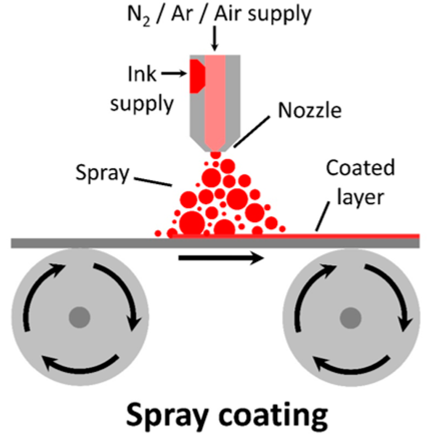
- Spray coating
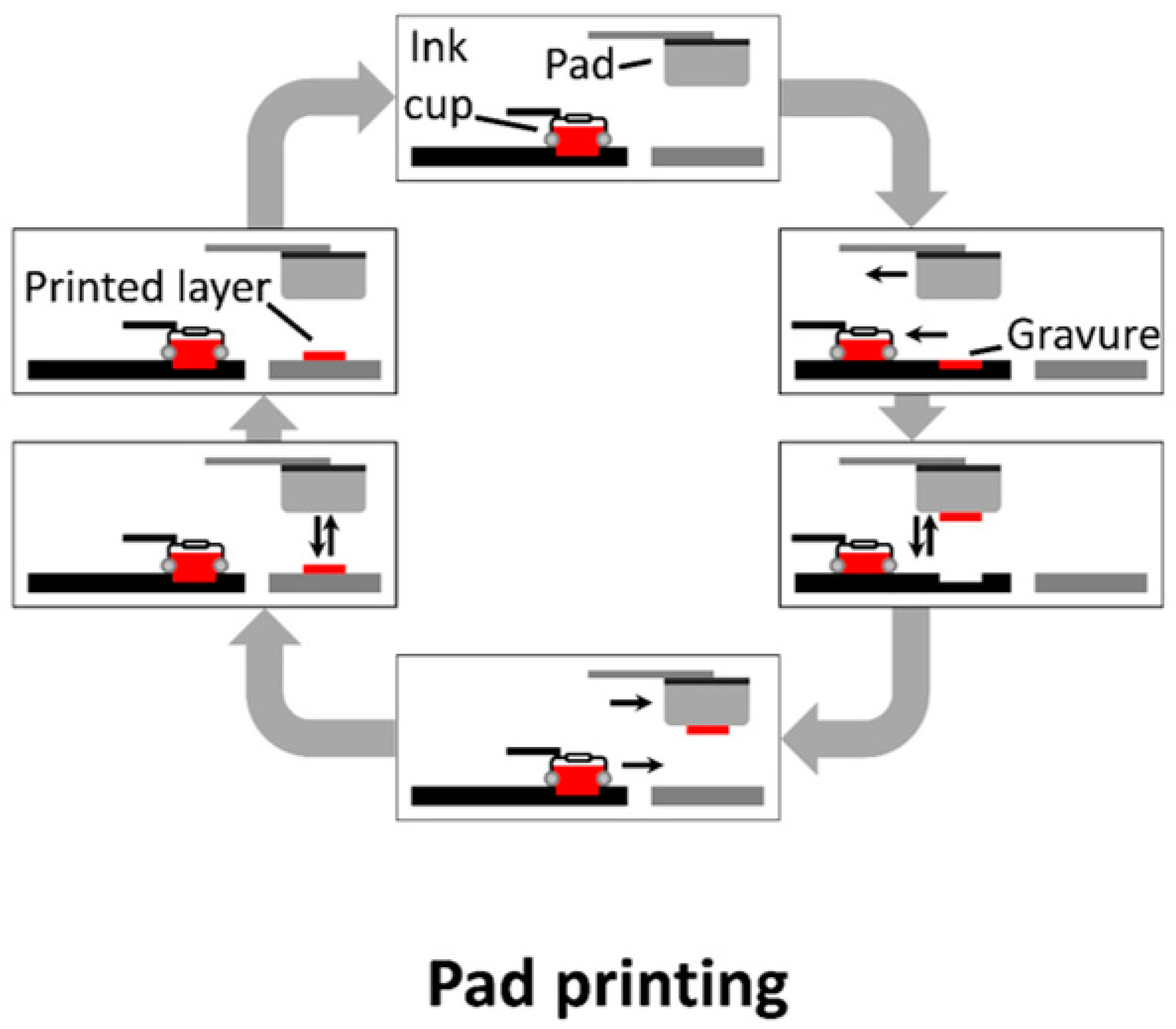
- Pad printing
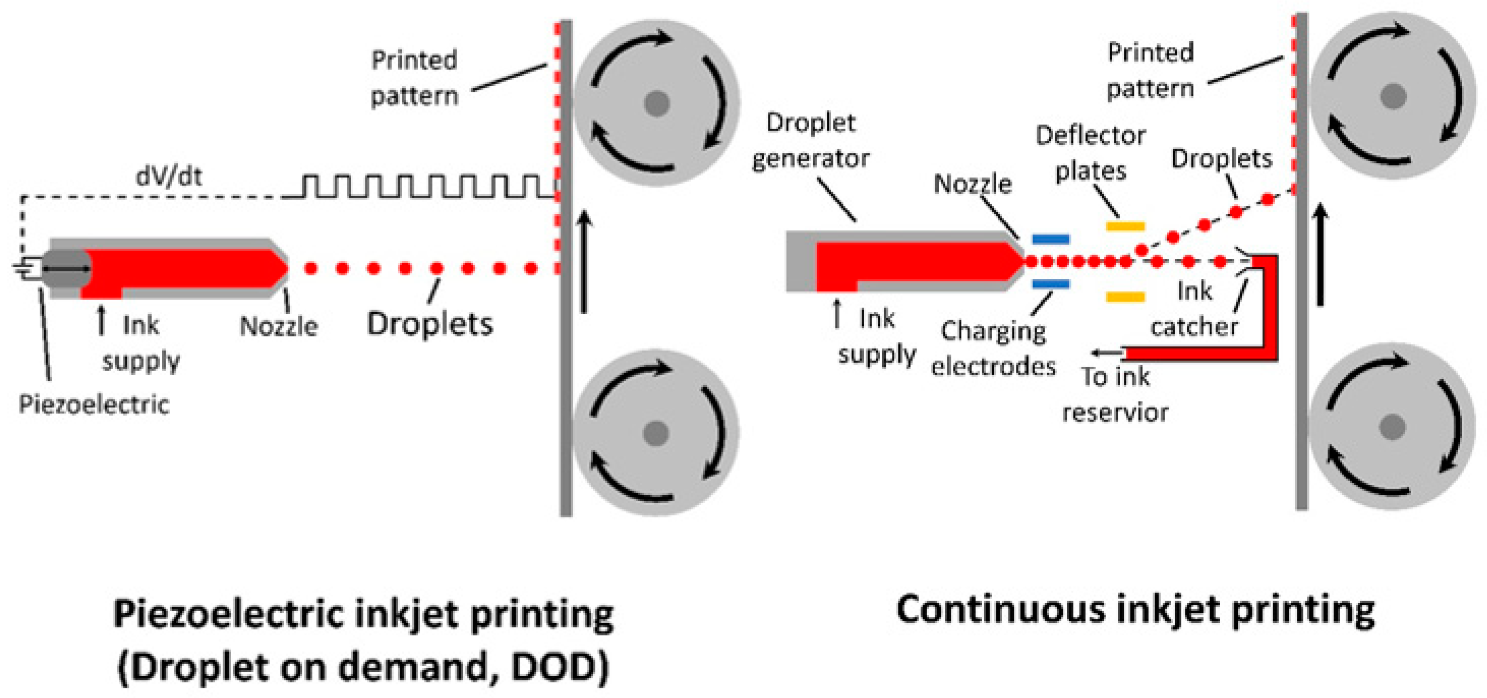
- Ink-jet printing
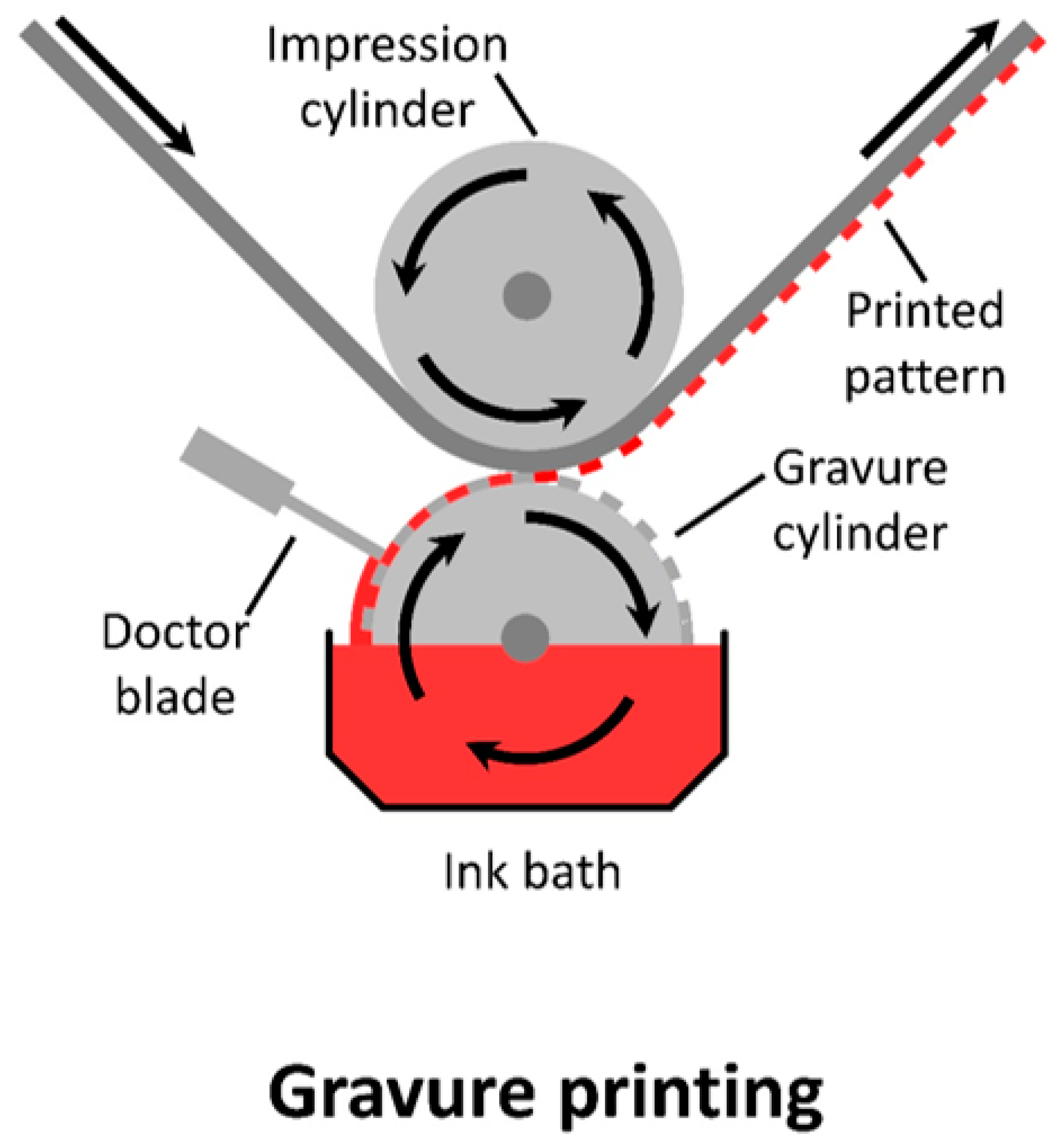
- Gravure printing
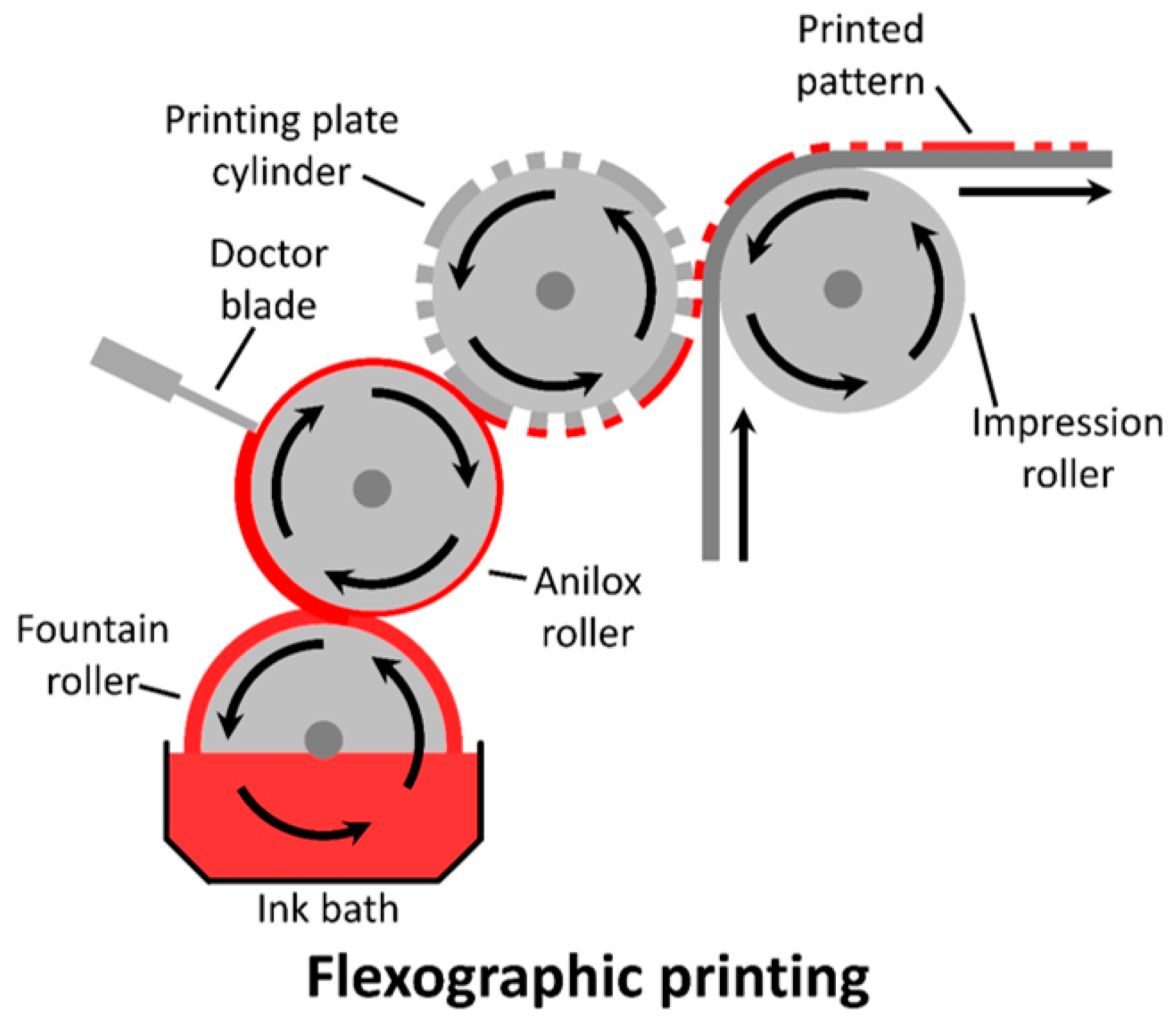
- Flexographic printing
- Screen printing
2. Background
3. Coating and Printing Techniques for OPV
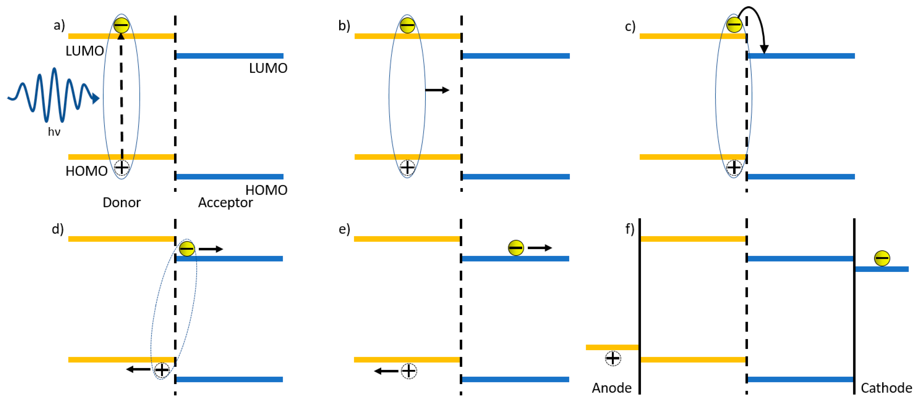
3.1. Vacuum and Non-Vacuum Deposition
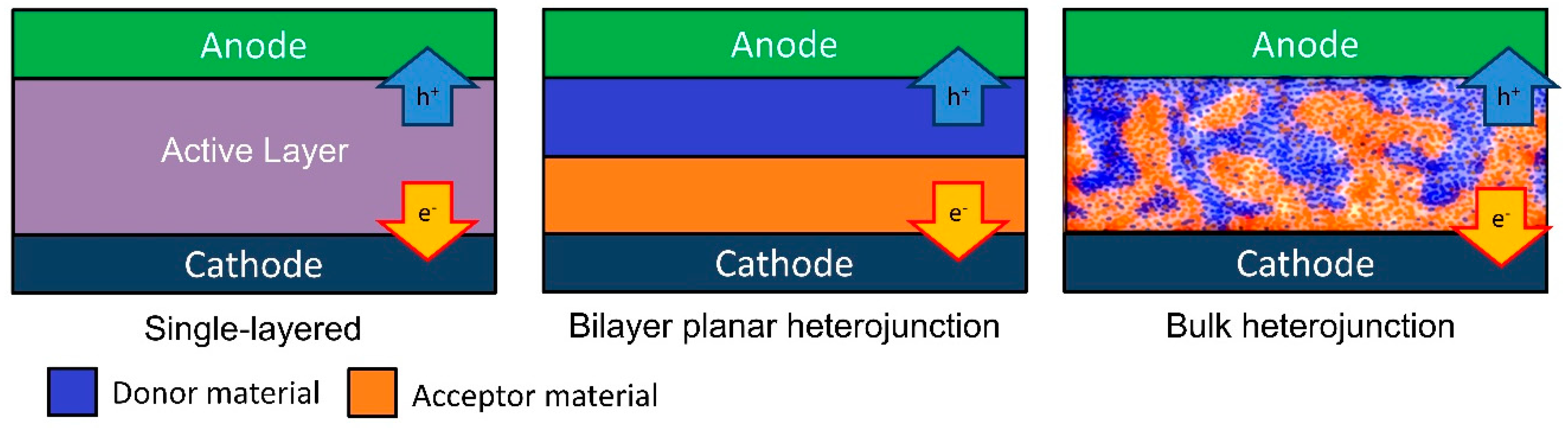
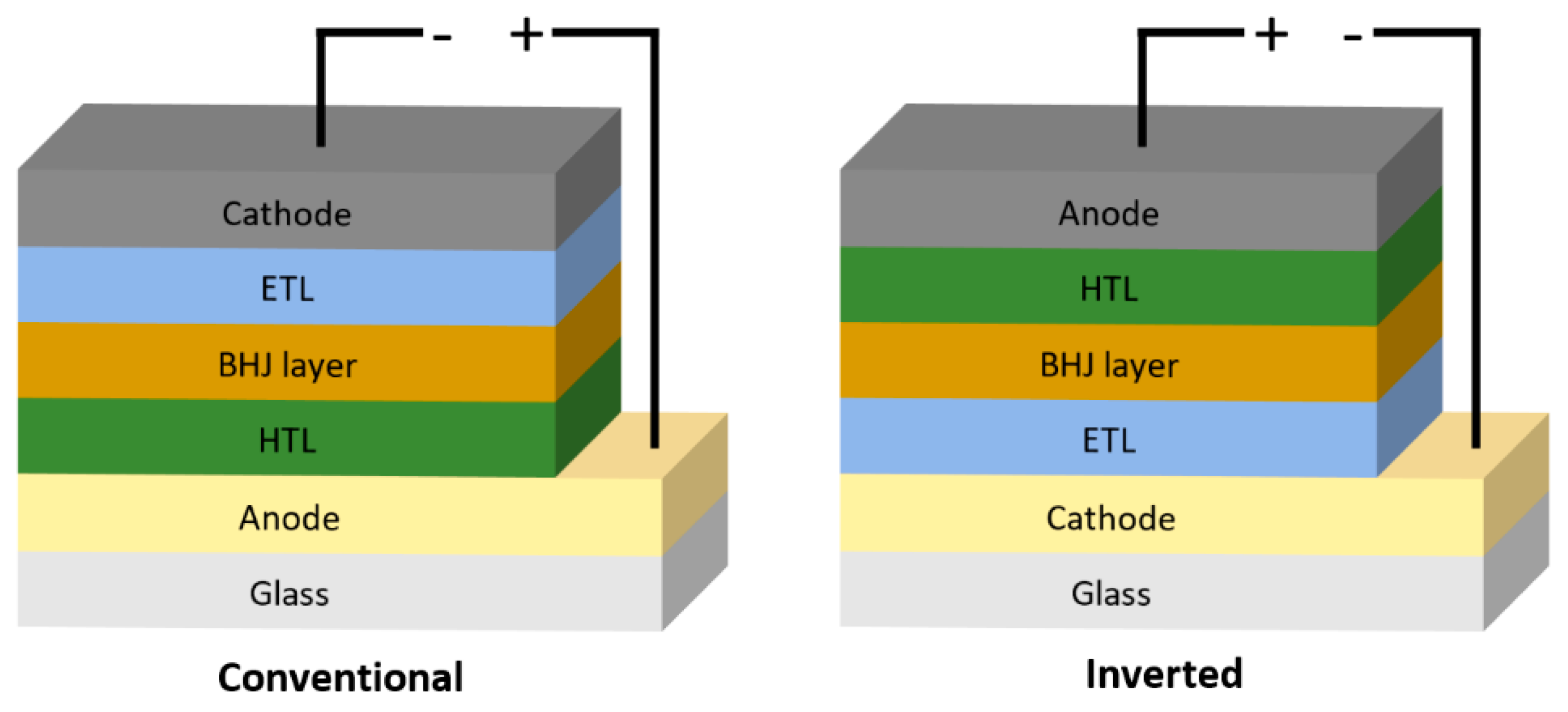
3.2. OPV Fabrication Scalability via Alternative Printing and Coating Techniques
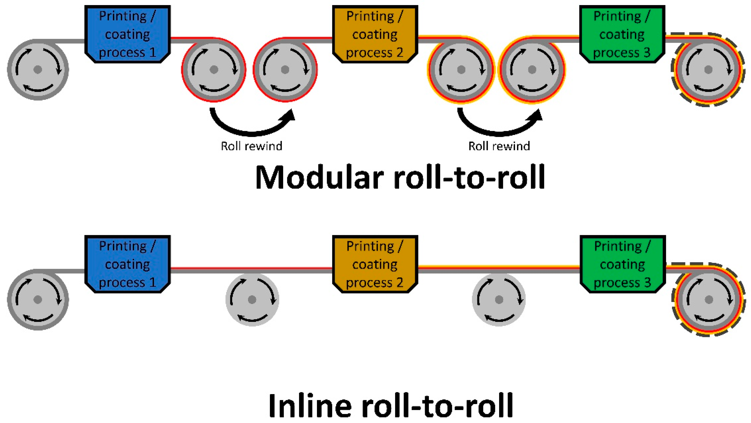
3.3. Roll-to-Roll Fabrication
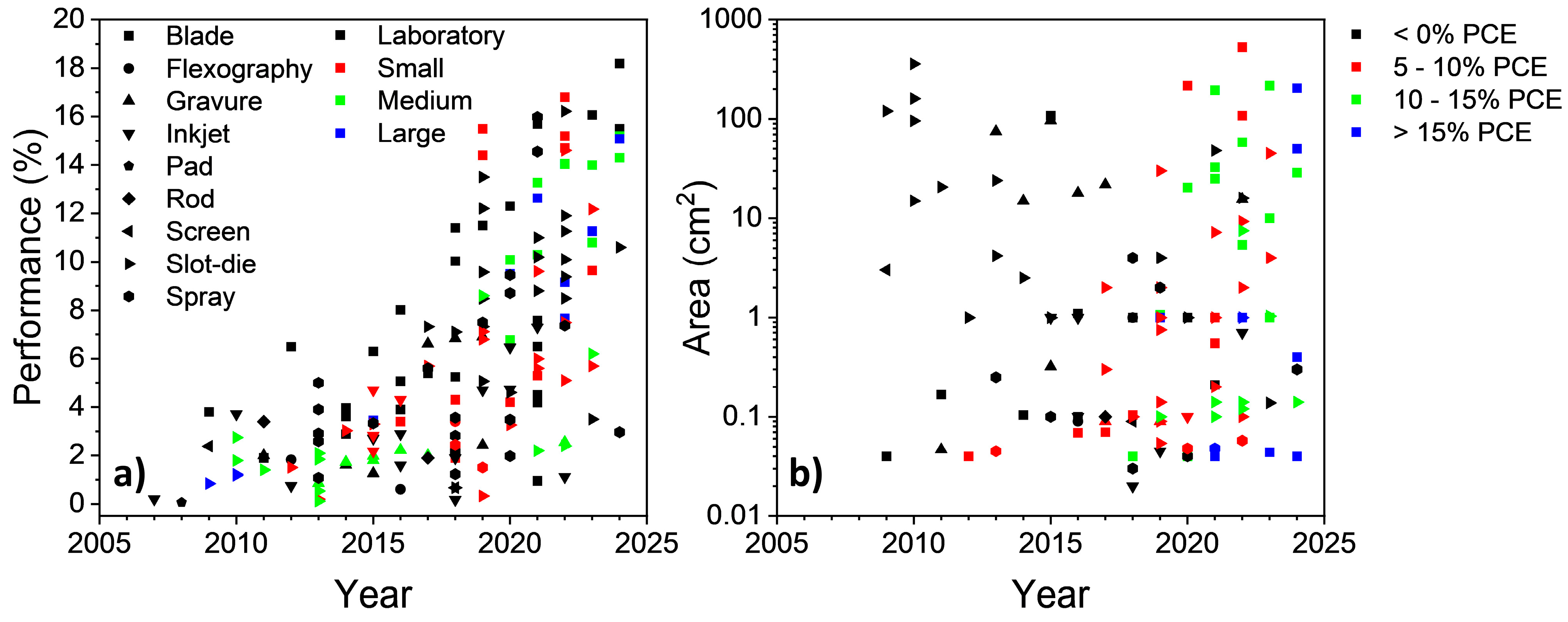
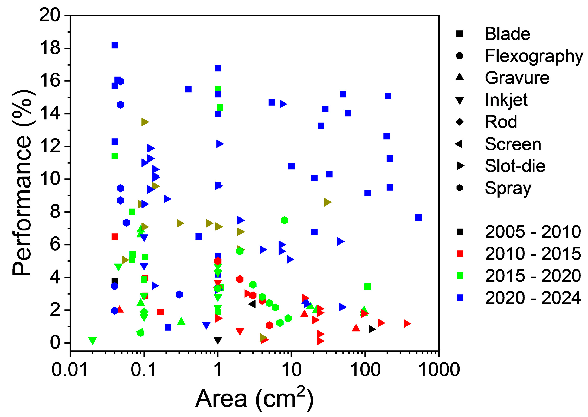
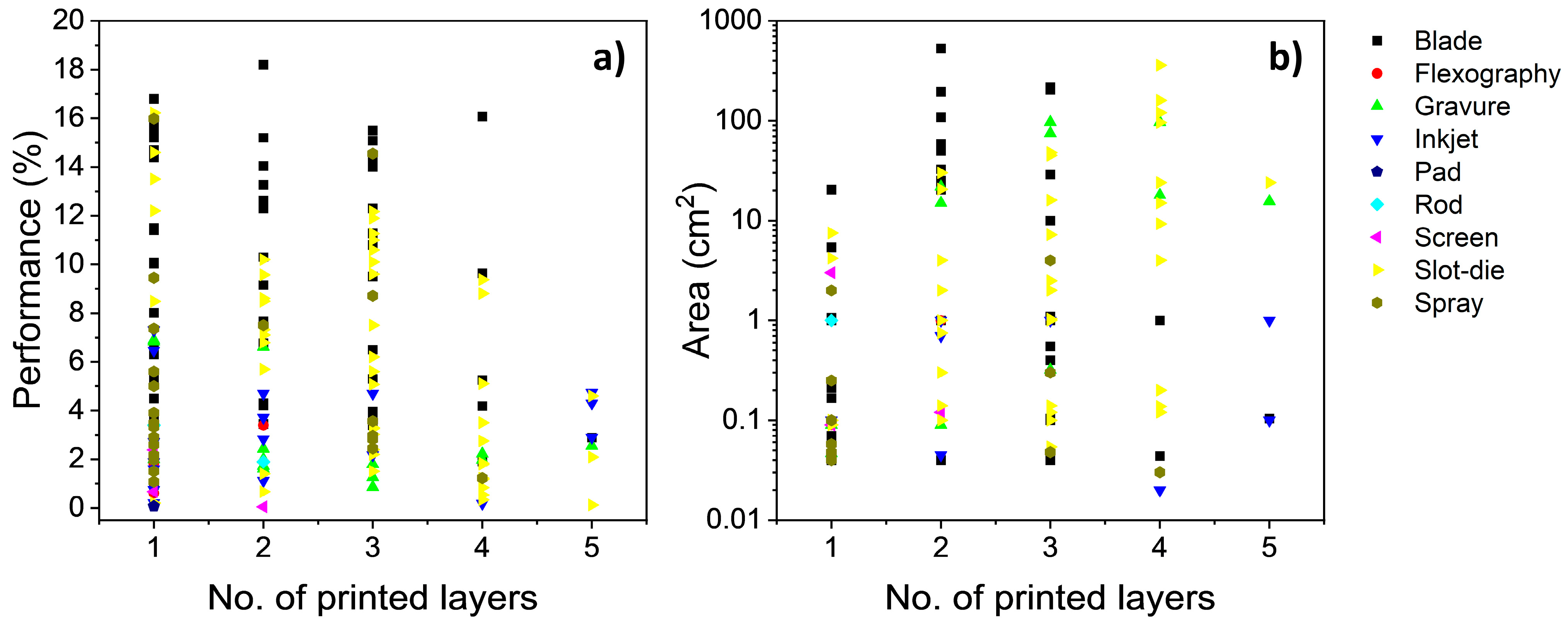
3.4. Types of Printing and Coating Methods
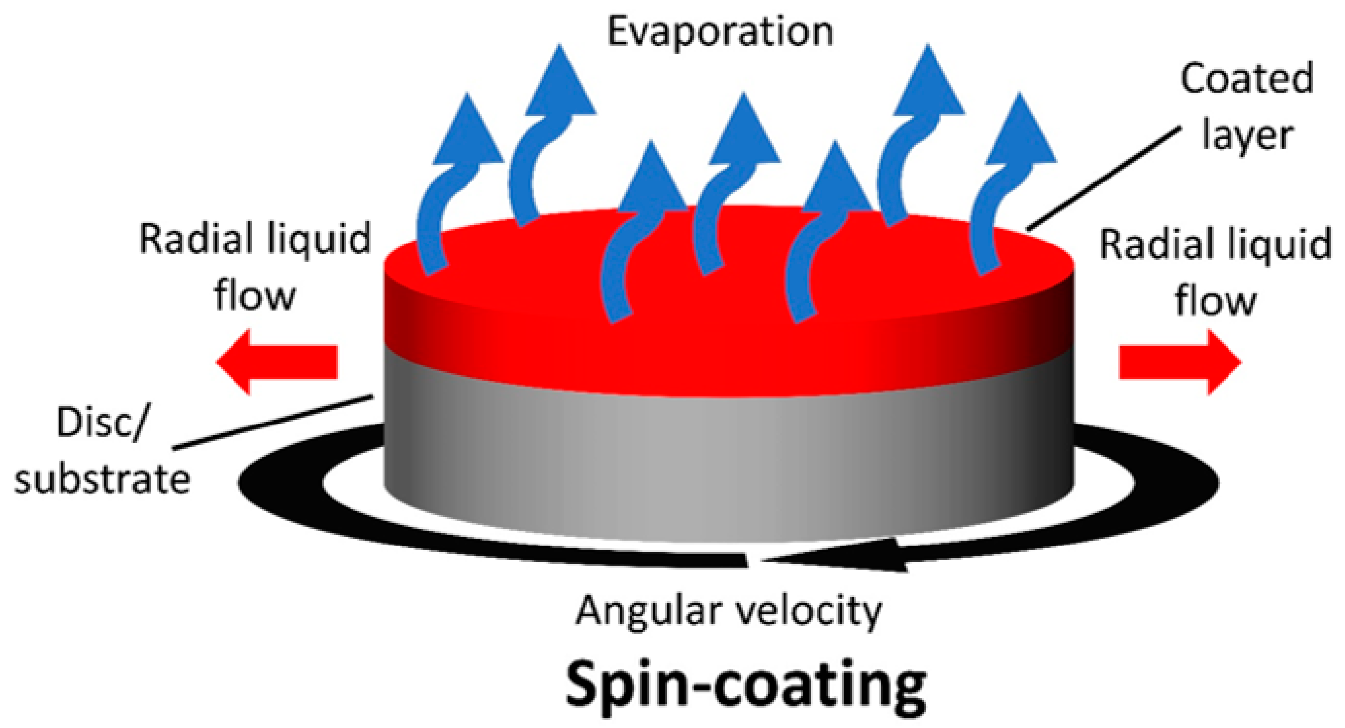
3.4.1. Spin Coating
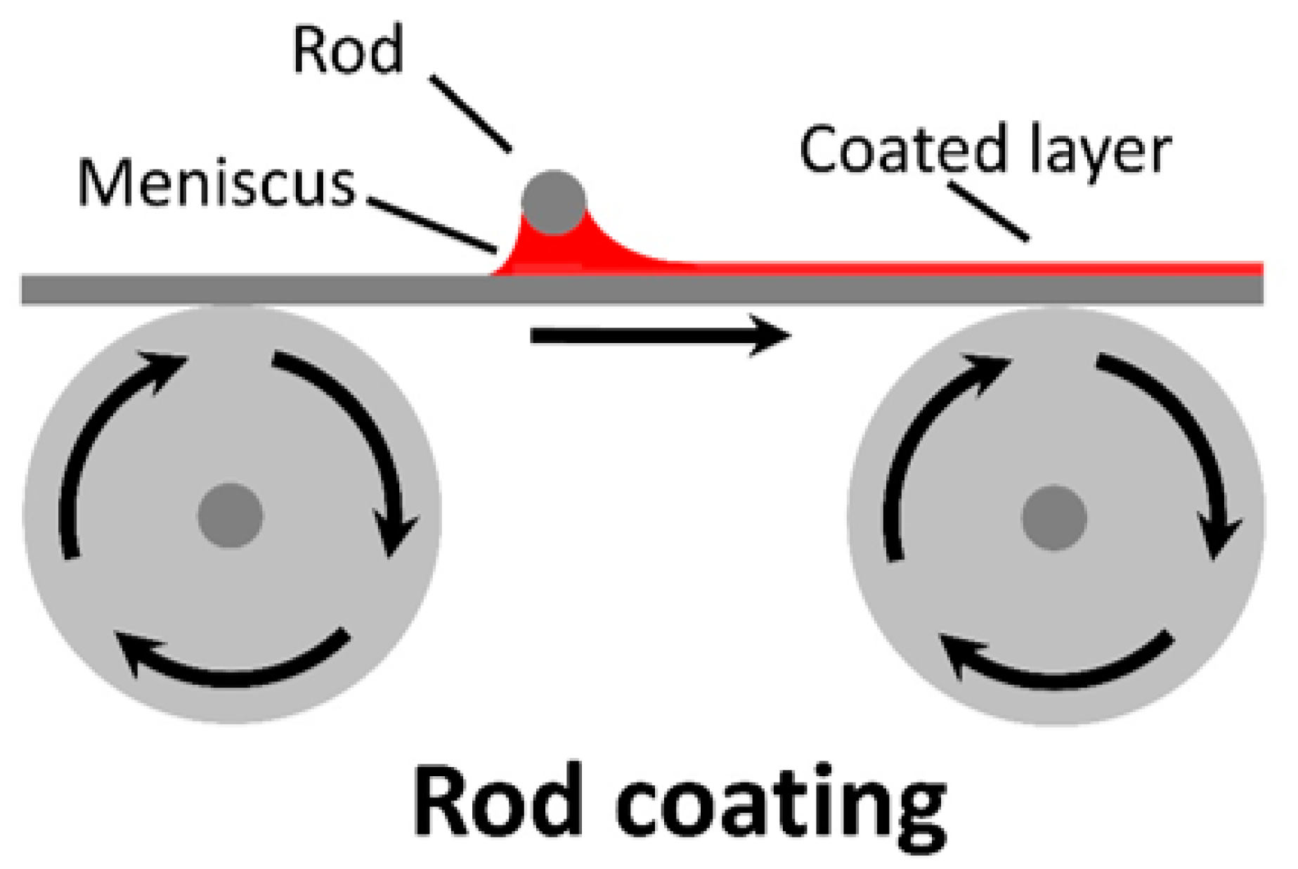
3.4.2. Rod Coating
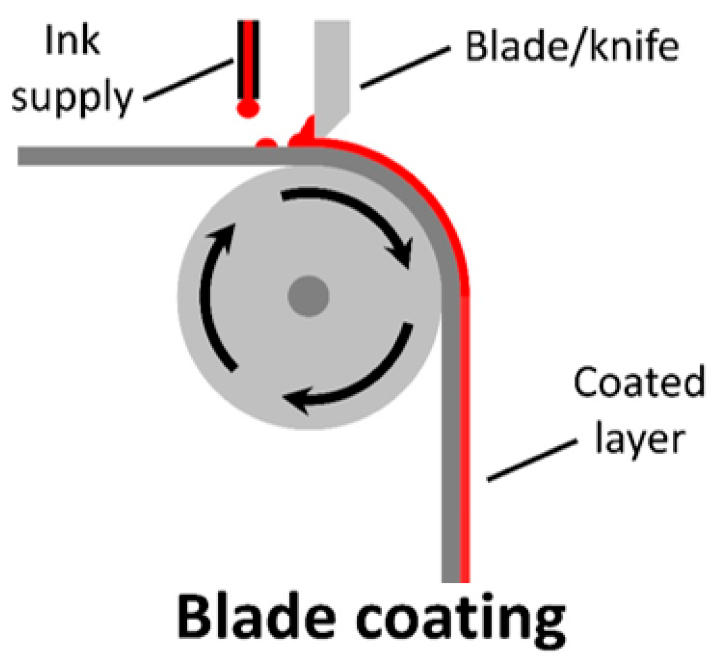
3.4.3. Blade Coating/Knife-over-Edge Coating/Doctor Blading
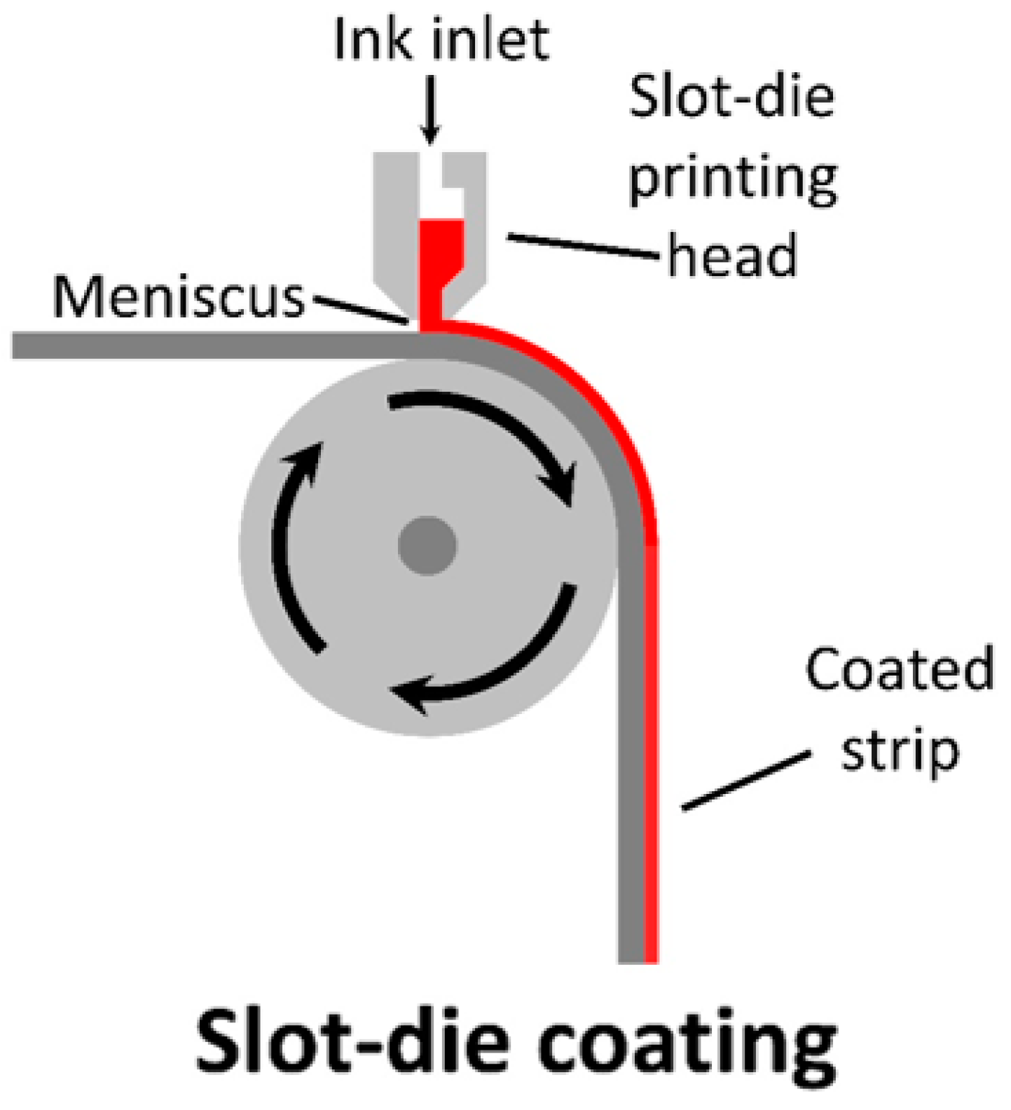
3.4.4. Slot-Die Coating
3.4.5. Spray Coating
3.4.6. Inkjet Printing
3.4.7. Pad Printing
3.4.8. Gravure Printing
3.4.9. Flexographic Printing
3.4.10. Screen Printing
3.5. Printing and Coating Method Comparison
4. Outlook
Author Contributions
Funding
Institutional Review Board Statement
Informed Consent Statement
Data Availability Statement
Conflicts of Interest
References
- Hussain, A.; Arif, S.M.; Aslam, M. Emerging renewable and sustainable energy technologies: State of the art. Renew. Sustain. Energy Rev. 2017, 71, 12–28. [Google Scholar] [CrossRef]
- Al-Shetwi, A.Q. Sustainable development of renewable energy integrated power sector: Trends, environmental impacts, and recent challenges. Sci. Total Environ. 2022, 822, 153645. [Google Scholar] [CrossRef]
- European Environment Agency. Renewable Energy in Europe—2017 Update; European Environment Agency: Copenhagen, Denmark, 2017. [Google Scholar]
- Johansson, T.B.; Kelly, H.; Reddy, A.K.; Williams, R.H. Renewable Energy: Sources for Fuels and Electricity; Island Press: Washington, DC, USA, 1993. [Google Scholar]
- Herzog, A.; Lipman, T.; Kammen, D. Renewable energy sources, Encyclopedia of Life Support Systems (EOLSS). In Forerunner Volume—Perspectives and Overview of Life Support Systems and Sustainable Development; UNESCO Publishing-Eolss Publishers: Oxford, UK, 2001. [Google Scholar]
- Ritchie, H.; Roser, M.; Rosado, P. Energy; Our World Data: Oxford, UK, 2022. [Google Scholar]
- Holliday, S.; Li, Y.; Luscombe, C.K. Recent advances in high performance donor-acceptor polymers for organic photovoltaics. Prog. Polym. Sci. 2017, 70, 34–51. [Google Scholar] [CrossRef]
- Yin, H.; Ho, J.K.W.; Cheung, S.H.; Yan, R.J.; Chiu, K.L.; Hao, X.; So, S.K. Designing a ternary photovoltaic cell for indoor light harvesting with a power conversion efficiency exceeding 20%. J. Mater. Chem. A 2018, 6, 8579–8585. [Google Scholar] [CrossRef]
- Cho, Y.; Kumari, T.; Jeong, S.; Lee, S.M.; Jeong, M.; Lee, B.; Oh, J.; Zhang, Y.; Huang, B.; Chen, L.; et al. Guest-oriented non-fullerene acceptors for ternary organic solar cells with over 16.0% and 22.7% efficiencies under one-sun and indoor light. Nano Energy 2020, 75, 104896. [Google Scholar] [CrossRef]
- Park, S.Y.; Labanti, C.; Luke, J.; Chin, Y.-C.; Kim, J.-S. Organic Bilayer Photovoltaics for Efficient Indoor Light Harvesting. Adv. Energy Mater. 2022, 12, 2103237. [Google Scholar] [CrossRef]
- Small, C.E.; Chen, S.; Subbiah, J.; Amb, C.M.; Tsang, S.-W.; Lai, T.-H.; Reynolds, J.R.; So, F. High-efficiency inverted dithienogermole–thienopyrrolodione-based polymer solar cells. Nat. Photonics 2012, 6, 115–120. [Google Scholar] [CrossRef]
- He, Z.; Zhong, C.; Huang, X.; Wong, W.Y.; Wu, H.; Chen, L.; Su, S.; Cao, Y. Simultaneous enhancement of open-circuit voltage, short-circuit current density, and fill factor in polymer solar cells. Adv. Mater. 2011, 23, 4636–4643. [Google Scholar] [CrossRef] [PubMed]
- Zhu, L.; Zhang, M.; Xu, J.; Li, C.; Yan, J.; Zhou, G.; Zhong, W.; Hao, T.; Song, J.; Xue, X.; et al. Single-junction organic solar cells with over 19% efficiency enabled by a refined double-fibril network morphology. Nat. Mater. 2022, 21, 656–663. [Google Scholar] [CrossRef]
- Ding, G.; Chen, T.; Wang, M.; Xia, X.; He, C.; Zheng, X.; Li, Y.; Zhou, D.; Lu, X.; Zuo, L.; et al. Solid Additive-Assisted Layer-by-Layer Processing for 19% Efficiency Binary Organic Solar Cells. Nano-Micro Lett. 2023, 15, 92. [Google Scholar] [CrossRef]
- Wei, Y.; Chen, Z.; Lu, G.; Yu, N.; Li, C.; Gao, J.; Gu, X.; Hao, X.; Lu, G.; Tang, Z.; et al. Binary Organic Solar Cells Breaking 19% via Manipulating the Vertical Component Distribution. Adv. Mater. 2022, 34, 2204718. [Google Scholar] [CrossRef] [PubMed]
- Basu, R.; Gumpert, F.; Lohbreier, J.; Morin, P.-O.; Vohra, V.; Liu, Y.; Zhou, Y.; Brabec, C.J.; Egelhaaf, H.-J.; Distler, A. Large-area organic photovoltaic modules with 14.5% certified world record efficiency. Joule 2024, 8, 970–978. [Google Scholar] [CrossRef]
- Chiang, C.K.; Fincher, C.R.; Park, Y.W.; Heeger, A.J.; Shirakawa, H.; Louis, E.J.; Gau, S.C.; MacDiarmid, A.G. Electrical Conductivity in Doped Polyacetylene. Phys. Rev. Lett. 1977, 39, 1098–1101. [Google Scholar] [CrossRef]
- Dou, L.; Liu, Y.; Hong, Z.; Li, G.; Yang, Y. Low-bandgap near-IR conjugated polymers/molecules for organic electronics. Chem. Rev. 2015, 115, 12633–12665. [Google Scholar] [CrossRef]
- Yiu, A.T.; Beaujuge, P.M.; Lee, O.P.; Woo, C.H.; Toney, M.F.; Frechet, J.M. Side-chain tunability of furan-containing low-band-gap polymers provides control of structural order in efficient solar cells. J. Am. Chem. Soc. 2012, 134, 2180–2185. [Google Scholar] [CrossRef] [PubMed]
- Kroto, H.W.; Heath, J.R.; O’Brien, S.C.; Curl, R.F.; Smalley, R.E. C60: Buckminsterfullerene. Nature 1985, 318, 162–163. [Google Scholar] [CrossRef]
- Yu, G.; Gao, J.; Hummelen, J.C.; Wudl, F.; Heeger, A.J. Polymer photovoltaic cells: Enhanced efficiencies via a network of internal donor-acceptor heterojunctions. Science 1995, 270, 1789–1791. [Google Scholar] [CrossRef]
- Wienk, M.M.; Kroon, J.M.; Verhees, W.J.H.; Knol, J.; Hummelen, J.C.; van Hal, P.A.; Janssen, R.A.J. Efficient Methano[70]fullerene/MDMO-PPV Bulk Heterojunction Photovoltaic Cells. Angew. Chem. Int. Ed. 2003, 42, 3371–3375. [Google Scholar] [CrossRef]
- Gurney, R.S.; Li, W.; Yan, Y.; Liu, D.; Pearson, A.J.; Wang, T. Morphology and efficiency enhancements of PTB7-Th: ITIC nonfullerene organic solar cells processed via solvent vapor annealing. J. Energy Chem. 2019, 37, 148–156. [Google Scholar] [CrossRef]
- Lin, Y.; Zhao, F.; He, Q.; Huo, L.; Wu, Y.; Parker, T.C.; Ma, W.; Sun, Y.; Wang, C.; Zhu, D. High-performance electron acceptor with thienyl side chains for organic photovoltaics. J. Am. Chem. Soc. 2016, 138, 4955–4961. [Google Scholar] [CrossRef]
- Lin, Y.; Zhan, X. Oligomer molecules for efficient organic photovoltaics. Acc. Chem. Res. 2016, 49, 175–183. [Google Scholar] [CrossRef] [PubMed]
- Chen, C.-P.; Tsai, Y.-Y.; Chen, Y.-C.; Li, Y.-H. High-performance and long-term stable inverted ternary solar cells based on PTB7-Th/N2200/PC71BM blends. Sol. Energy 2018, 176, 170–177. [Google Scholar] [CrossRef]
- Yuan, J.; Guo, W.; Xia, Y.; Ford, M.J.; Jin, F.; Liu, D.; Zhao, H.; Inganäs, O.; Bazan, G.C.; Ma, W. Comparing the device physics, dynamics and morphology of polymer solar cells employing conventional PCBM and non-fullerene polymer acceptor N2200. Nano Energy 2017, 35, 251–262. [Google Scholar] [CrossRef]
- Jiang, B.-H.; Chen, C.-P.; Liang, H.-T.; Jeng, R.-J.; Chien, W.-C.; Yu, Y.-Y. The role of Y6 as the third component in fullerene-free ternary organic photovoltaics. Dye. Pigment. 2020, 181, 108613. [Google Scholar] [CrossRef]
- Wang, R.; Zhang, C.; Li, Q.; Zhang, Z.; Wang, X.; Xiao, M. Charge separation from an intra-moiety intermediate state in the high-performance PM6: Y6 organic photovoltaic blend. J. Am. Chem. Soc. 2020, 142, 12751–12759. [Google Scholar] [CrossRef] [PubMed]
- Lv, J.; Tang, H.; Huang, J.; Yan, C.; Liu, K.; Yang, Q.; Hu, D.; Singh, R.; Lee, J.; Lu, S. Additive-induced miscibility regulation and hierarchical morphology enable 17.5% binary organic solar cells. Energy Environ. Sci. 2021, 14, 3044–3052. [Google Scholar] [CrossRef]
- Mcleskey, J.T., Jr. Device architectures in organic photovoltaics. Turk. J. Phys. 2014, 38, 516–525. [Google Scholar] [CrossRef]
- Pierini, F.; Lanzi, M.; Nakielski, P.; Pawłowska, S.; Urbanek, O.; Zembrzycki, K.; Kowalewski, T.A. Single-material organic solar cells based on electrospun fullerene-grafted polythiophene nanofibers. Macromolecules 2017, 50, 4972–4981. [Google Scholar] [CrossRef]
- Wu, Y.; Guo, J.; Wang, W.; Chen, Z.; Chen, Z.; Sun, R.; Wu, Q.; Wang, T.; Hao, X.; Zhu, H. A conjugated donor-acceptor block copolymer enables over 11% efficiency for single-component polymer solar cells. Joule 2021, 5, 1800–1815. [Google Scholar] [CrossRef]
- Guo, J.; Wu, Y.; Wang, W.; Wang, T.; Min, J. Achieving 12.6% Efficiency in Single-Component Organic Solar Cells Processed from Nonhalogenated Solvents. Sol. RRL 2022, 6, 2101024. [Google Scholar] [CrossRef]
- Liang, S.; Xiao, C.; Xie, C.; Liu, B.; Fang, H.; Li, W. 13% Single-Component Organic Solar Cells based on Double-Cable Conjugated Polymers with Pendent Y-Series Acceptors. Adv. Mater. 2023, 35, 2300629. [Google Scholar] [CrossRef] [PubMed]
- Brabec, C.J.; Sariciftci, N.S.; Hummelen, J.C. Plastic solar cells. Adv. Funct. Mater. 2001, 11, 15–26. [Google Scholar] [CrossRef]
- Halls, J.; Walsh, C.; Greenham, N.C.; Marseglia, E.; Friend, R.H.; Moratti, S.; Holmes, A. Efficient photodiodes from interpenetrating polymer networks. Nature 1995, 376, 498. [Google Scholar] [CrossRef]
- Fontana, M.; Kang, H.; Yee, P.Y.; Fan, Z.; Hawks, S.A.; Schelhas, L.T.; Subramaniyan, S.; Hwang, Y.-J.; Jenekhe, S.A.; Tolbert, S.H. Low-Vapor-Pressure Solvent Additives Function as Polymer Swelling Agents in Bulk Heterojunction Organic Photovoltaics. J. Phys. Chem. C 2018, 122, 16574–16588. [Google Scholar] [CrossRef]
- Lee, K.H.; Schwenn, P.E.; Smith, A.R.G.; Cavaye, H.; Shaw, P.E.; James, M.; Krueger, K.B.; Gentle, I.R.; Meredith, P.; Burn, P.L. Morphology of All-Solution-Processed “Bilayer” Organic Solar Cells. Adv. Mater. 2011, 23, 766–770. [Google Scholar] [CrossRef] [PubMed]
- Seok, J.; Shin, T.J.; Park, S.; Cho, C.; Lee, J.-Y.; Yeol Ryu, D.; Kim, M.H.; Kim, K. Efficient Organic Photovoltaics Utilizing Nanoscale Heterojunctions in Sequentially Deposited Polymer/fullerene Bilayer. Sci. Rep. 2015, 5, 8373. [Google Scholar] [CrossRef] [PubMed]
- Hong, M.; Youn, J.; Ryu, K.Y.; Shafian, S.; Kim, K. Improving the Stability of Non-fullerene-Based Organic Photovoltaics through Sequential Deposition and Utilization of a Quasi-orthogonal Solvent. ACS Appl. Mater. Interfaces 2023, 15, 20151–20158. [Google Scholar] [CrossRef]
- Sun, R.; Wang, T.; Yang, X.; Wu, Y.; Wang, Y.; Wu, Q.; Zhang, M.; Brabec, C.J.; Li, Y.; Min, J. High-speed sequential deposition of photoactive layers for organic solar cell manufacturing. Nat. Energy 2022, 7, 1087–1099. [Google Scholar] [CrossRef]
- Zhang, W.; Zhao, B.; He, Z.; Zhao, X.; Wang, H.; Yang, S.; Wu, H.; Cao, Y. High-efficiency ITO-free polymer solar cells using highly conductive PEDOT: PSS/surfactant bilayer transparent anodes. Energy Environ. Sci. 2013, 6, 1956–1964. [Google Scholar] [CrossRef]
- Andersen, T.R.; Cooling, N.A.; Almyahi, F.; Hart, A.S.; Nicolaidis, N.C.; Feron, K.; Noori, M.; Vaughan, B.; Griffith, M.J.; Belcher, W.J.; et al. Fully roll-to-roll prepared organic solar cells in normal geometry with a sputter-coated aluminium top-electrode. Sol. Energy Mater. Sol. Cells 2016, 149, 103–109. [Google Scholar] [CrossRef]
- Hu, Z.; Zhang, J.; Hao, Z.; Zhao, Y. Influence of doped PEDOT: PSS on the performance of polymer solar cells. Sol. Energy Mater. Sol. Cells 2011, 95, 2763–2767. [Google Scholar] [CrossRef]
- Khodabakhsh, S.; Sanderson, B.M.; Nelson, J.; Jones, T.S. Using self-assembling dipole molecules to improve charge collection in molecular solar cells. Adv. Funct. Mater. 2006, 16, 95–100. [Google Scholar] [CrossRef]
- Jonda, C.; Mayer, A.; Stolz, U.; Elschner, A.; Karbach, A. Surface roughness effects and their influence on the degradation of organic light emitting devices. J. Mater. Sci. 2000, 35, 5645–5651. [Google Scholar] [CrossRef]
- Malliaras, G.; Salem, J.; Brock, P.; Scott, J. Photovoltaic measurement of the built-in potential in organic light emitting diodes and photodiodes. J. Appl. Phys. 1998, 84, 1583–1587. [Google Scholar] [CrossRef]
- Benanti, T.L.; Venkataraman, D. Organic solar cells: An overview focusing on active layer morphology. Photosynth. Res. 2006, 87, 73–81. [Google Scholar] [CrossRef] [PubMed]
- Kim, Y.; Ballantyne, A.M.; Nelson, J.; Bradley, D.D. Effects of thickness and thermal annealing of the PEDOT: PSS layer on the performance of polymer solar cells. Org. Electron. 2009, 10, 205–209. [Google Scholar] [CrossRef]
- Chen, X.; Zhao, C.; Rothberg, L.; Ng, M.-K. Plasmon enhancement of bulk heterojunction organic photovoltaic devices by electrode modification. Appl. Phys. Lett. 2008, 93, 344. [Google Scholar] [CrossRef]
- Jørgensen, M.; Norrman, K.; Gevorgyan, S.A.; Tromholt, T.; Andreasen, B.; Krebs, F.C. Stability of Polymer Solar Cells. Adv. Mater. 2012, 24, 580–612. [Google Scholar] [CrossRef]
- Po, R.; Bernardi, A.; Calabrese, A.; Carbonera, C.; Corso, G.; Pellegrino, A. From lab to fab: How must the polymer solar cell materials design change?—An industrial perspective. Energy Environ. Sci. 2014, 7, 925–943. [Google Scholar] [CrossRef]
- Huang, J.; Yin, Z.; Zheng, Q. Applications of ZnO in organic and hybrid solar cells. Energy Environ. Sci. 2011, 4, 3861–3877. [Google Scholar] [CrossRef]
- White, M.-S.; Olson, D.; Shaheen, S.; Kopidakis, N.; Ginley, D.S. Inverted bulk-heterojunction organic photovoltaic device using a solution-derived ZnO underlayer. Appl. Phys. Lett. 2006, 89, 143517. [Google Scholar] [CrossRef]
- Park, S.H.; Roy, A.; Beaupré, S.; Cho, S.; Coates, N.; Moon, J.S.; Moses, D.; Leclerc, M.; Lee, K.; Heeger, A.J. Bulk heterojunction solar cells with internal quantum efficiency approaching 100%. Nat. Photonics 2009, 3, 297–302. [Google Scholar] [CrossRef]
- Xiong, J.; Yang, B.; Zhou, C.; Yang, J.; Duan, H.; Huang, W.; Zhang, X.; Xia, X.; Zhang, L.; Huang, H. Enhanced efficiency and stability of polymer solar cells with TiO2 nanoparticles buffer layer. Org. Electron. 2014, 15, 835–843. [Google Scholar] [CrossRef]
- Bob, B.; Song, T.-B.; Chen, C.-C.; Xu, Z.; Yang, Y. Nanoscale dispersions of gelled SnO2: Material properties and device applications. Chem. Mater. 2013, 25, 4725–4730. [Google Scholar] [CrossRef]
- Niazi, M.R.; Munir, R.; D’Souza, R.M.; Kelly, T.L.; Welch, G.C. Scalable Non-Halogenated Co-solvent System for Large-Area, Four-Layer Slot-Die-Coated Organic Photovoltaics. ACS Appl. Mater. Interfaces 2022, 14, 57055–57063. [Google Scholar] [CrossRef] [PubMed]
- Chang, Y.-M.; Liao, C.-Y.; Lee, C.-C.; Lin, S.-Y.; Teng, N.-W.; Huei-Shuan Tan, P. All solution and ambient processable organic photovoltaic modules fabricated by slot-die coating and achieved a certified 7.56% power conversion efficiency. Sol. Energy Mater. Sol. Cells 2019, 202, 110064. [Google Scholar] [CrossRef]
- Wang, J.; Xu, L.; Zhang, B.; Lee, Y.J.; Hsu, J.W. n-Type doping induced by electron transport layer in organic photovoltaic devices. Adv. Electron. Mater. 2017, 3, 1600458. [Google Scholar] [CrossRef]
- Andersen, T.R.; Almyahi, F.; Cooling, N.A.; Elkington, D.; Wiggins, L.; Fahy, A.; Feron, K.; Vaughan, B.; Griffith, M.J.; Mozer, A.J. Comparison of inorganic electron transport layers in fully roll-to-roll coated/printed organic photovoltaics in normal geometry. J. Mater. Chem. A 2016, 4, 15986–15996. [Google Scholar] [CrossRef]
- Song, S.; Lee, K.T.; Koh, C.W.; Shin, H.; Gao, M.; Woo, H.Y.; Vak, D.; Kim, J.Y. Hot slot die coating for additive-free fabrication of high performance roll-to-roll processed polymer solar cells. Energy Environ. Sci. 2018, 11, 3248–3255. [Google Scholar] [CrossRef]
- Ylikunnari, M.; Välimäki, M.; Väisänen, K.-L.; Kraft, T.M.; Sliz, R.; Corso, G.; Po, R.; Barbieri, R.; Carbonera, C.; Gorni, G.; et al. Flexible OPV modules for highly efficient indoor applications. Flex. Print. Electron. 2020, 5, 014008. [Google Scholar] [CrossRef]
- Zhao, H.; Zhang, L.; Naveed, H.B.; Lin, B.; Zhao, B.; Zhou, K.; Gao, C.; Zhang, C.; Wang, C.; Ma, W. Processing-Friendly Slot-Die-Cast Nonfullerene Organic Solar Cells with Optimized Morphology. ACS Appl. Mater. Interfaces 2019, 11, 42392–42402. [Google Scholar] [CrossRef]
- Zhang, Y.-X.; Fang, J.; Li, W.; Shen, Y.; Chen, J.-D.; Li, Y.; Gu, H.; Pelivani, S.; Zhang, M.; Li, Y.; et al. Synergetic Transparent Electrode Architecture for Efficient Non-Fullerene Flexible Organic Solar Cells with >12% Efficiency. ACS Nano 2019, 13, 4686–4694. [Google Scholar] [CrossRef]
- Dayneko, S.V.; Pahlevani, M.; Welch, G.C. Indoor Photovoltaics: Photoactive Material Selection, Greener Ink Formulations, and Slot-Die Coated Active Layers. ACS Appl. Mater. Interfaces 2019, 11, 46017–46025. [Google Scholar] [CrossRef]
- Jasieniak, J.J.; Seifter, J.; Jo, J.; Mates, T.; Heeger, A.J. A Solution-Processed MoOx Anode Interlayer for Use within Organic Photovoltaic Devices. Adv. Funct. Mater. 2012, 22, 2594–2605. [Google Scholar] [CrossRef]
- Ki, T.; Lee, C.; Kim, J.; Hwang, I.-W.; Oh, C.-M.; Park, K.; Lee, S.; Kim, J.-H.; Balamurugan, C.; Kong, J.; et al. Anion-Induced Catalytic Reaction in a Solution-Processed Molybdenum Oxide for Efficient Inverted Ternary Organic Photovoltaics. Adv. Funct. Mater. 2022, 32, 2204493. [Google Scholar] [CrossRef]
- Yang, H.-C.; Zha, W.; Weng, C.-N.; Chen, C.-H.; Zan, H.-W.; Su, K.-W.; Luo, Q.; Ma, C.-Q.; Chao, Y.-C.; Meng, H.-F. Vacuum-free fabrication of organic solar cell on assembled glass substrates. Opt. Mater. 2021, 112, 110683. [Google Scholar] [CrossRef]
- Chiang, W.-T.; Su, S.-H.; Lin, Y.-F.; Yokoyama, M. Increasing the fill factor and power conversion efficiency of polymer photovoltaic cell using V2O5/CuPc as a buffer layer. Jpn. J. Appl. Phys. 2010, 49, 04DK14. [Google Scholar] [CrossRef]
- Wang, H.-Q.; Li, N.; Guldal, N.S.; Brabec, C.J. Nanocrystal V2O5 thin film as hole-extraction layer in normal architecture organic solar cells. Org. Electron. 2012, 13, 3014–3021. [Google Scholar] [CrossRef]
- Li, S.-S.; Tu, K.-H.; Lin, C.-C.; Chen, C.-W.; Chhowalla, M. Solution-processable graphene oxide as an efficient hole transport layer in polymer solar cells. ACS Nano 2010, 4, 3169–3174. [Google Scholar] [CrossRef]
- Murray, I.P.; Lou, S.J.; Cote, L.J.; Loser, S.; Kadleck, C.J.; Xu, T.; Szarko, J.M.; Rolczynski, B.S.; Johns, J.E.; Huang, J. Graphene oxide interlayers for robust, high-efficiency organic photovoltaics. J. Phys. Chem. Lett. 2011, 2, 3006–3012. [Google Scholar] [CrossRef]
- Widjonarko, N.E.; Ratcliff, E.L.; Perkins, C.L.; Sigdel, A.K.; Zakutayev, A.; Ndione, P.F.; Gillaspie, D.T.; Ginley, D.S.; Olson, D.C.; Berry, J.J. Sputtered nickel oxide thin film for efficient hole transport layer in polymer–fullerene bulk-heterojunction organic solar cell. Thin Solid Film. 2012, 520, 3813–3818. [Google Scholar] [CrossRef]
- Steirer, K.X.; Ndione, P.F.; Widjonarko, N.E.; Lloyd, M.T.; Meyer, J.; Ratcliff, E.L.; Kahn, A.; Armstrong, N.R.; Curtis, C.J.; Ginley, D.S. Enhanced efficiency in plastic solar cells via energy matched solution processed NiOx interlayers. Adv. Energy Mater. 2011, 1, 813–820. [Google Scholar] [CrossRef]
- Li, M.; Zhang, W.; Wang, H.; Chen, L.; Zheng, C.; Chen, R. Effect of organic cathode interfacial layers on efficiency and stability improvement of polymer solar cells. RSC Adv. 2017, 7, 31158–31163. [Google Scholar] [CrossRef]
- Kundu, S.; Gollu, S.R.; Sharma, R.; Srinivas, G.; Ashok, A.; Kulkarni, A.; Gupta, D. Device stability of inverted and conventional bulk heterojunction solar cells with MoO3 and ZnO nanoparticles as charge transport layers. Org. Electron. 2013, 14, 3083–3088. [Google Scholar] [CrossRef]
- Hau, S.K.; Yip, H.-L.; Baek, N.S.; Zou, J.; O’Malley, K.; Jen, A.K.-Y. Air-stable inverted flexible polymer solar cells using zinc oxide nanoparticles as an electron selective layer. Appl. Phys. Lett. 2008, 92, 253301. [Google Scholar] [CrossRef]
- Lloyd, M.T.; Olson, D.C.; Lu, P.; Fang, E.; Moore, D.L.; White, M.S.; Reese, M.O.; Ginley, D.S.; Hsu, J.W. Impact of contact evolution on the shelf life of organic solar cells. J. Mater. Chem. 2009, 19, 7638–7642. [Google Scholar] [CrossRef]
- Distler, A.; Brabec, C.J.; Egelhaaf, H.-J. Organic photovoltaic modules with new world record efficiencies. Prog. Photovolt. Res. Appl. 2021, 29, 24–31. [Google Scholar] [CrossRef]
- Alem, S.; Graddage, N.; Lu, J.; Kololuoma, T.; Movileanu, R.; Tao, Y. Flexographic printing of polycarbazole-based inverted solar cells. Org. Electron. 2018, 52, 146–152. [Google Scholar] [CrossRef]
- Takahira, K.; Toda, A.; Suzuki, K.; Fukuda, T. Highly efficient organic photovoltaic cells fabricated by electrospray deposition using a non-halogenated solution. Phys. Status Solidi (A) 2017, 214, 1600536. [Google Scholar] [CrossRef]
- Tsai, P.-T.; Yu, K.-C.; Chang, C.-J.; Horng, S.-F.; Meng, H.-F. Large-area organic solar cells by accelerated blade coating. Org. Electron. 2015, 22, 166–172. [Google Scholar] [CrossRef]
- Hernandez, J.L.; Deb, N.; Wolfe, R.M.W.; Lo, C.K.; Engmann, S.; Richter, L.J.; Reynolds, J.R. Simple transfer from spin coating to blade coating through processing aggregated solutions. J. Mater. Chem. A 2017, 5, 20687–20695. [Google Scholar] [CrossRef]
- Huang, Y.-C.; Cha, H.-C.; Chen, C.-Y.; Tsao, C.-S. A universal roll-to-roll slot-die coating approach towards high-efficiency organic photovoltaics. Prog. Photovolt. Res. Appl. 2017, 25, 928–935. [Google Scholar] [CrossRef]
- Lee, J.; Seo, Y.-H.; Kwon, S.-N.; Kim, D.-H.; Jang, S.; Jung, H.; Lee, Y.; Weerasinghe, H.; Kim, T.; Kim, J.Y.; et al. Slot-Die and Roll-to-Roll Processed Single Junction Organic Photovoltaic Cells with the Highest Efficiency. Adv. Energy Mater. 2019, 9, 1901805. [Google Scholar] [CrossRef]
- Kirk, B.; Pan, X.; Jevric, M.; Andersson, G.; Andersson, M.R. Introducing neat fullerenes to improve the thermal stability of slot-die coated organic solar cells. Mater. Adv. 2022, 3, 2838–2849. [Google Scholar] [CrossRef]
- Iannaccone, G.; Välimäki, M.; Jansson, E.; Sunnari, A.; Corso, G.; Bernardi, A.; Levi, M.; Turri, S.; Hast, J.; Griffini, G. Roll-to-roll compatible flexible polymer solar cells incorporating a water-based solution-processable silver back electrode with low annealing temperature. Sol. Energy Mater. Sol. Cells 2015, 143, 227–235. [Google Scholar] [CrossRef]
- Krebs, F.C.; Tromholt, T.; Jørgensen, M. Upscaling of polymer solar cell fabrication using full roll-to-roll processing. Nanoscale 2010, 2, 873–886. [Google Scholar] [CrossRef]
- Garg, A.; Gupta, S.K.; Jasieniak, J.J.; Singh, T.B.; Watkins, S.E. Improved lifetimes of organic solar cells with solution-processed molybdenum oxide anode-modifying layers. Prog. Photovolt. Res. Appl. 2015, 23, 989–996. [Google Scholar] [CrossRef]
- Lima, F.A.S.; Beliatis, M.J.; Roth, B.; Andersen, T.R.; Bortoti, A.; Reyna, Y.; Castro, E.; Vasconcelos, I.F.; Gevorgyan, S.A.; Krebs, F.C.; et al. Flexible ITO-free organic solar cells applying aqueous solution-processed V2O5 hole transport layer: An outdoor stability study. APL Mater. 2016, 4, 026104. [Google Scholar] [CrossRef]
- La Notte, L.; Bianco, G.V.; Palma, A.L.; Di Carlo, A.; Bruno, G.; Reale, A. Sprayed organic photovoltaic cells and mini-modules based on chemical vapor deposited graphene as transparent conductive electrode. Carbon 2018, 129, 878–883. [Google Scholar] [CrossRef]
- Lee, C.-Y.; Tsao, C.-S.; Lin, H.-K.; Cha, H.-C.; Chung, T.-Y.; Sung, Y.-M.; Huang, Y.-C. Encapsulation improvement and stability of ambient roll-to-roll slot-die-coated organic photovoltaic modules. Sol. Energy 2021, 213, 136–144. [Google Scholar]
- Camarada, M.B.; Saldías, C.; Castro-Castillo, C.; Angel, F.A. Evaluation of electro-synthesized oligothiophenes as donor materials in vacuum-processed organic photovoltaic devices. Mater. Lett. 2023, 339, 134114. [Google Scholar] [CrossRef]
- Xi, X.; Li, W.; Wu, J.; Ji, J.; Shi, Z.; Li, G. A comparative study on the performances of small molecule organic solar cells based on CuPc/C60 and CuPc/C70. Sol. Energy Mater. Sol. Cells 2010, 94, 2435–2441. [Google Scholar] [CrossRef]
- Yagui, J.; Angel, F.A. Benzodithiophene-based small molecules for vacuum-processed organic photovoltaic devices. Opt. Mater. 2020, 109, 110354. [Google Scholar] [CrossRef]
- Chen, C.-H.; Ting, H.-C.; Li, Y.-Z.; Lo, Y.-C.; Sher, P.-H.; Wang, J.-K.; Chiu, T.-L.; Lin, C.-F.; Hsu, I.S.; Lee, J.-H.; et al. New D–A–A-Configured Small-Molecule Donors for High-Efficiency Vacuum-Processed Organic Photovoltaics under Ambient Light. ACS Appl. Mater. Interfaces 2019, 11, 8337–8349. [Google Scholar] [CrossRef] [PubMed]
- Griffith, M.J.; Cooling, N.A.; Vaughan, B.; O’Donnell, K.M.; Al-Mudhaffer, M.F.; Al-Ahmad, A.; Noori, M.; Almyahi, F.; Belcher, W.J.; Dastoor, P.C. Roll-to-Roll Sputter Coating of Aluminum Cathodes for Large-Scale Fabrication of Organic Photovoltaic Devices. Energy Technol. 2015, 3, 428–436. [Google Scholar] [CrossRef]
- Willmann, J.; Stocker, D.; Dörsam, E. Characteristics and evaluation criteria of substrate-based manufacturing. Is roll-to-roll the best solution for printed electronics? Org. Electron. 2014, 15, 1631–1640. [Google Scholar] [CrossRef]
- Chang, Y.-H.; Tseng, S.-R.; Chen, C.-Y.; Meng, H.-F.; Chen, E.-C.; Horng, S.-F.; Hsu, C.-S. Polymer solar cell by blade coating. Org. Electron. 2009, 10, 741–746. [Google Scholar] [CrossRef]
- Lim, F.J.; Ananthanarayanan, K.; Luther, J.; Ho, G.W. Influence of a novel fluorosurfactant modified PEDOT:PSS hole transport layer on the performance of inverted organic solar cells. J. Mater. Chem. 2012, 22, 25057–25064. [Google Scholar] [CrossRef]
- Kapnopoulos, C.; Mekeridis, E.D.; Tzounis, L.; Polyzoidis, C.; Zachariadis, A.; Tsimikli, S.; Gravalidis, C.; Laskarakis, A.; Vouroutzis, N.; Logothetidis, S. Fully gravure printed organic photovoltaic modules: A straightforward process with a high potential for large scale production. Sol. Energy Mater. Sol. Cells 2016, 144, 724–731. [Google Scholar] [CrossRef]
- Hoff, A.; Gasonoo, A.; Pahlevani, M.; Welch, G.C. An Alcohol-Soluble N-Annulated Perylene Diimide Cathode Interlayer for Air-Processed, Slot-Die Coated Organic Photovoltaic Devices and Large-Area Modules. Sol. RRL 2022, 6, 2200691. [Google Scholar] [CrossRef]
- Zardetto, V.; Brown, T.M.; Reale, A.; Di Carlo, A. Substrates for flexible electronics: A practical investigation on the electrical, film flexibility, optical, temperature, and solvent resistance properties. J. Polym. Sci. Part B Polym. Phys. 2011, 49, 638–648. [Google Scholar] [CrossRef]
- Qu, B.; Forrest, S.R. Continuous roll-to-roll fabrication of organic photovoltaic cells via interconnected high-vacuum and low-pressure organic vapor phase deposition systems. Appl. Phys. Lett. 2018, 113, 053302. [Google Scholar] [CrossRef]
- Lucera, L.; Machui, F.; Kubis, P.; Schmidt, H.D.; Adams, J.; Strohm, S.; Ahmad, T.; Forberich, K.; Egelhaaf, H.J.; Brabec, C.J. Highly efficient, large area, roll coated flexible and rigid OPV modules with geometric fill factors up to 98.5% processed with commercially available materials. Energy Environ. Sci. 2016, 9, 89–94. [Google Scholar] [CrossRef]
- Lee, H.; Lee, D.; Jeong, H. Mechanical aspects of the chemical mechanical polishing process: A review. Int. J. Precis. Eng. Manuf. 2016, 17, 525–536. [Google Scholar] [CrossRef]
- Park, J.; Shin, K.; Lee, C. Improvement of cross-machine directional thickness deviation for uniform pressure-sensitive adhesive layer in roll-to-roll slot-die coating process. Int. J. Precis. Eng. Manuf. 2015, 16, 937–943. [Google Scholar] [CrossRef]
- Pettersson, L.A.A.; Roman, L.S.; Inganäs, O. Modeling photocurrent action spectra of photovoltaic devices based on organic thin films. J. Appl. Phys. 1999, 86, 487–496. [Google Scholar] [CrossRef]
- Deledalle, F.; Kirchartz, T.; Vezie, M.S.; Campoy-Quiles, M.; Shakya Tuladhar, P.; Nelson, J.; Durrant, J.R. Understanding the Effect of Unintentional Doping on Transport Optimization and Analysis in Efficient Organic Bulk-Heterojunction Solar Cells. Phys. Rev. X 2015, 5, 011032. [Google Scholar] [CrossRef]
- Kirchartz, T.; Agostinelli, T.; Campoy-Quiles, M.; Gong, W.; Nelson, J. Understanding the Thickness-Dependent Performance of Organic Bulk Heterojunction Solar Cells: The Influence of Mobility, Lifetime, and Space Charge. J. Phys. Chem. Lett. 2012, 3, 3470–3475. [Google Scholar] [CrossRef]
- Destouesse, E.; Top, M.; Lamminaho, J.; Rubahn, H.G.; Fahlteich, J.; Madsen, M. Slot-die processing and encapsulation of non-fullerene based ITO-free organic solar cells and modules. Flex. Print. Electron. 2019, 4, 045004. [Google Scholar] [CrossRef]
- Krebs, F.C.; Fyenbo, J.; Jørgensen, M. Product integration of compact roll-to-roll processed polymer solar cell modules: Methods and manufacture using flexographic printing, slot-die coating and rotary screen printing. J. Mater. Chem. 2010, 20, 8994–9001. [Google Scholar] [CrossRef]
- Hösel, M.; Søndergaard, R.R.; Jørgensen, M.; Krebs, F.C. Fast Inline Roll-to-Roll Printing for Indium-Tin-Oxide-Free Polymer Solar Cells Using Automatic Registration. Energy Technol. 2013, 1, 102–107. [Google Scholar] [CrossRef]
- Bao, S.; Yang, H.; Fan, H.; Zhang, J.; Wei, Z.; Cui, C.; Li, Y. Volatilizable Solid Additive-Assisted Treatment Enables Organic Solar Cells with Efficiency over 18.8% and Fill Factor Exceeding 80%. Adv. Mater. 2021, 33, 2105301. [Google Scholar] [CrossRef] [PubMed]
- An, Q.; Wang, J.; Gao, W.; Ma, X.; Hu, Z.; Gao, J.; Xu, C.; Hao, M.; Zhang, X.; Yang, C.; et al. Alloy-like ternary polymer solar cells with over 17.2% efficiency. Sci. Bull. 2020, 65, 538–545. [Google Scholar] [CrossRef] [PubMed]
- Liu, Q.; Jiang, Y.; Jin, K.; Qin, J.; Xu, J.; Li, W.; Xiong, J.; Liu, J.; Xiao, Z.; Sun, K. 18% Efficiency organic solar cells. Sci. Bull. 2020, 65, 272–275. [Google Scholar] [CrossRef] [PubMed]
- Krebs, F.C. Fabrication and processing of polymer solar cells: A review of printing and coating techniques. Sol. Energy Mater. Sol. Cells 2009, 93, 394–412. [Google Scholar] [CrossRef]
- Chen, D.; Nakahara, A.; Wei, D.; Nordlund, D.; Russell, T.P. P3HT/PCBM bulk heterojunction organic photovoltaics: Correlating efficiency and morphology. Nano Lett. 2011, 11, 561–567. [Google Scholar] [CrossRef] [PubMed]
- Vanlaeke, P.; Swinnen, A.; Haeldermans, I.; Vanhoyland, G.; Aernouts, T.; Cheyns, D.; Deibel, C.; D’Haen, J.; Heremans, P.; Poortmans, J. P3HT/PCBM bulk heterojunction solar cells: Relation between morphology and electro-optical characteristics. Sol. Energy Mater. Sol. Cells 2006, 90, 2150–2158. [Google Scholar] [CrossRef]
- Zhao, J.; Swinnen, A.; Van Assche, G.; Manca, J.; Vanderzande, D.; Mele, B.V. Phase diagram of P3HT/PCBM blends and its implication for the stability of morphology. J. Phys. Chem. B 2009, 113, 1587–1591. [Google Scholar] [CrossRef] [PubMed]
- Zhang, L.; Lin, B.; Hu, B.; Xu, X.; Ma, W. Blade-Cast Nonfullerene Organic Solar Cells in Air with Excellent Morphology, Efficiency, and Stability. Adv. Mater. 2018, 30, 1800343. [Google Scholar] [CrossRef]
- Zhao, W.; Qian, D.; Zhang, S.; Li, S.; Inganäs, O.; Gao, F.; Hou, J. Fullerene-free polymer solar cells with over 11% efficiency and excellent thermal stability. Adv. Mater. 2016, 28, 4734–4739. [Google Scholar] [CrossRef]
- Liang, Q.; Han, J.; Song, C.; Yu, X.; Smilgies, D.-M.; Zhao, K.; Liu, J.; Han, Y. Reducing the confinement of PBDB-T to ITIC to improve the crystallinity of PBDB-T/ITIC blends. J. Mater. Chem. A 2018, 6, 15610–15620. [Google Scholar] [CrossRef]
- Perdigón-Toro, L.; Zhang, H.; Markina, A.; Yuan, J.; Hosseini, S.M.; Wolff, C.M.; Zuo, G.; Stolterfoht, M.; Zou, Y.; Gao, F. Barrierless free charge generation in the high-performance PM6: Y6 bulk heterojunction non-fullerene solar cell. Adv. Mater. 2020, 32, 1906763. [Google Scholar] [CrossRef] [PubMed]
- Lin, Y.; Adilbekova, B.; Firdaus, Y.; Yengel, E.; Faber, H.; Sajjad, M.; Zheng, X.; Yarali, E.; Seitkhan, A.; Bakr, O.M. 17% efficient organic solar cells based on liquid exfoliated WS2 as a replacement for PEDOT: PSS. Adv. Mater. 2019, 31, 1902965. [Google Scholar] [CrossRef] [PubMed]
- Barrera, D.; Lee, Y.-J.; Hsu, J.W. Influence of ZnO sol–gel electron transport layer processing on BHJ active layer morphology and OPV performance. Sol. Energy Mater. Sol. Cells 2014, 125, 27–32. [Google Scholar] [CrossRef]
- Zhang, C.; You, H.; Lin, Z.; Hao, Y. Inverted organic photovoltaic cells with solution-processed zinc oxide as electron collecting layer. Jpn. J. Appl. Phys. 2011, 50, 082302. [Google Scholar] [CrossRef]
- Jagadamma, L.K.; Al-Senani, M.; El-Labban, A.; Gereige, I.; Ngongang Ndjawa, G.O.; Faria, J.C.; Kim, T.; Zhao, K.; Cruciani, F.; Anjum, D.H. Polymer solar cells with efficiency > 10% enabled via a facile solution-processed Al-doped ZnO electron transporting layer. Adv. Energy Mater. 2015, 5, 1500204. [Google Scholar] [CrossRef]
- Jiang, Z.; Soltanian, S.; Gholamkhass, B.; Aljaafari, A.; Servati, P. Light-soaking free organic photovoltaic devices with sol–gel deposited ZnO and AZO electron transport layers. RSC Adv. 2018, 8, 36542–36548. [Google Scholar] [CrossRef]
- Murdoch, G.; Hinds, S.; Sargent, E.; Tsang, S.; Mordoukhovski, L.; Lu, Z. Aluminum doped zinc oxide for organic photovoltaics. Appl. Phys. Lett. 2009, 94, 138. [Google Scholar] [CrossRef]
- Cameron, J.; Skabara, P.J. The damaging effects of the acidity in PEDOT: PSS on semiconductor device performance and solutions based on non-acidic alternatives. Mater. Horiz. 2020, 7, 1759–1772. [Google Scholar] [CrossRef]
- Park, H.; Shi, Y.; Kong, J. Application of solvent modified PEDOT: PSS to graphene electrodes in organic solar cells. Nanoscale 2013, 5, 8934–8939. [Google Scholar] [CrossRef]
- Søndergaard, R.; Hösel, M.; Angmo, D.; Larsen-Olsen, T.T.; Krebs, F.C. Roll-to-roll fabrication of polymer solar cells. Mater. Today 2012, 15, 36–49. [Google Scholar] [CrossRef]
- Zhu, R.; Chung, C.-H.; Cha, K.C.; Yang, W.; Zheng, Y.B.; Zhou, H.; Song, T.-B.; Chen, C.-C.; Weiss, P.S.; Li, G.; et al. Fused Silver Nanowires with Metal Oxide Nanoparticles and Organic Polymers for Highly Transparent Conductors. ACS Nano 2011, 5, 9877–9882. [Google Scholar] [CrossRef] [PubMed]
- Tsai, C.-Y.; Lin, Y.-H.; Chang, Y.-M.; Kao, J.-C.; Liang, Y.-C.; Liu, C.-C.; Qiu, J.; Wu, L.; Liao, C.-Y.; Tan, H.-S.; et al. Large area organic photovoltaic modules fabricated on a 30 cm by 20 cm substrate with a power conversion efficiency of 9.5%. Sol. Energy Mater. Sol. Cells 2020, 218, 110762. [Google Scholar] [CrossRef]
- Välimäki, M.; Apilo, P.; Po, R.; Jansson, E.; Bernardi, A.; Ylikunnari, M.; Vilkman, M.; Corso, G.; Puustinen, J.; Tuominen, J.; et al. R2R-printed inverted OPV modules–towards arbitrary patterned designs. Nanoscale 2015, 7, 9570–9580. [Google Scholar] [CrossRef]
- Miranda, B.H.; Corrêa, L.d.Q.; Soares, G.A.; Martins, J.L.; Lopes, P.L.; Vilela, M.L.; Rodrigues, J.F.; Cunha, T.G.; Vilaça, R.d.Q.; Castro-Hermosa, S. Efficient fully roll-to-roll coated encapsulated organic solar module for indoor applications. Sol. Energy 2021, 220, 343–353. [Google Scholar] [CrossRef]
- Liao, C.-Y.; Hsiao, Y.-T.; Tsai, K.-W.; Teng, N.-W.; Li, W.-L.; Wu, J.-L.; Kao, J.-C.; Lee, C.-C.; Yang, C.-M.; Tan, H.-S.; et al. Photoactive Material for Highly Efficient and All Solution-Processed Organic Photovoltaic Modules: Study on the Efficiency, Stability, and Synthetic Complexity. Sol. RRL 2021, 5, 2000749. [Google Scholar] [CrossRef]
- Guo, F.; Kubis, P.; Stubhan, T.; Li, N.; Baran, D.; Przybilla, T.; Spiecker, E.; Forberich, K.; Brabec, C.J. Fully Solution-Processing Route toward Highly Transparent Polymer Solar Cells. ACS Appl. Mater. Interfaces 2014, 6, 18251–18257. [Google Scholar] [CrossRef] [PubMed]
- Pérez-Gutiérrez, E.; Lozano, J.; Gaspar-Tánori, J.; Maldonado, J.-L.; Gómez, B.; López, L.; Amores-Tapia, L.-F.; Barbosa-García, O.; Percino, M.-J. Organic solar cells all made by blade and slot–die coating techniques. Sol. Energy 2017, 146, 79–84. [Google Scholar] [CrossRef]
- Sankaran, S.; Glaser, K.; Gärtner, S.; Rödlmeier, T.; Sudau, K.; Hernandez-Sosa, G.; Colsmann, A. Fabrication of polymer solar cells from organic nanoparticle dispersions by doctor blading or ink-jet printing. Org. Electron. 2016, 28, 118–122. [Google Scholar] [CrossRef]
- Strohm, S.; Machui, F.; Langner, S.; Kubis, P.; Gasparini, N.; Salvador, M.; McCulloch, I.; Egelhaaf, H.J.; Brabec, C.J. P3HT: Non-fullerene acceptor based large area, semi-transparent PV modules with power conversion efficiencies of 5%, processed by industrially scalable methods. Energy Environ. Sci. 2018, 11, 2225–2234. [Google Scholar] [CrossRef]
- Ye, L.; Xiong, Y.; Yao, H.; Gadisa, A.; Zhang, H.; Li, S.; Ghasemi, M.; Balar, N.; Hunt, A.; O’Connor, B.T.; et al. High Performance Organic Solar Cells Processed by Blade Coating in Air from a Benign Food Additive Solution. Chem. Mater. 2016, 28, 7451–7458. [Google Scholar] [CrossRef]
- Tait, J.G.; Merckx, T.; Li, W.; Wong, C.; Gehlhaar, R.; Cheyns, D.; Turbiez, M.; Heremans, P. Determination of Solvent Systems for Blade Coating Thin Film Photovoltaics. Adv. Funct. Mater. 2015, 25, 3393–3398. [Google Scholar] [CrossRef]
- Hong, L.; Yao, H.; Wu, Z.; Cui, Y.; Zhang, T.; Xu, Y.; Yu, R.; Liao, Q.; Gao, B.; Xian, K.; et al. Eco-Compatible Solvent-Processed Organic Photovoltaic Cells with Over 16% Efficiency. Adv. Mater. 2019, 31, 1903441. [Google Scholar] [CrossRef] [PubMed]
- Liao, C.-Y.; Chen, Y.; Lee, C.-C.; Wang, G.; Teng, N.-W.; Lee, C.-H.; Li, W.-L.; Chen, Y.-K.; Li, C.-H.; Ho, H.-L.; et al. Processing Strategies for an Organic Photovoltaic Module with over 10% Efficiency. Joule 2020, 4, 189–206. [Google Scholar] [CrossRef]
- Zhao, W.; Zhang, S.; Zhang, Y.; Li, S.; Liu, X.; He, C.; Zheng, Z.; Hou, J. Environmentally Friendly Solvent-Processed Organic Solar Cells that are Highly Efficient and Adaptable for the Blade-Coating Method. Adv. Mater. 2018, 30, 1704837. [Google Scholar] [CrossRef] [PubMed]
- Sundaresan, C.; Alem, S.; Radford, C.L.; Grant, T.M.; Kelly, T.L.; Lu, J.; Tao, Y.; Lessard, B.H. Changes in Optimal Ternary Additive Loading when Processing Large Area Organic Photovoltaics by Spin- versus Blade-Coating Methods. Sol. RRL 2021, 5, 2100432. [Google Scholar] [CrossRef]
- Schneider, A.; Traut, N.; Hamburger, M. Analysis and optimization of relevant parameters of blade coating and gravure printing processes for the fabrication of highly efficient organic solar cells. Sol. Energy Mater. Sol. Cells 2014, 126, 149–154. [Google Scholar] [CrossRef]
- Cui, Y.; Yao, H.; Hong, L.; Zhang, T.; Tang, Y.; Lin, B.; Xian, K.; Gao, B.; An, C.; Bi, P.; et al. Organic photovoltaic cell with 17% efficiency and superior processability. Natl. Sci. Rev. 2019, 7, 1239–1246. [Google Scholar] [CrossRef] [PubMed]
- Schneider, S.A.; Gu, K.L.; Yan, H.; Abdelsamie, M.; Bao, Z.; Toney, M.F. Controlling Polymer Morphology in Blade-Coated All-Polymer Solar Cells. Chem. Mater. 2021, 33, 5951–5961. [Google Scholar] [CrossRef]
- Hong, S.; Park, B.; Balamurugan, C.; Lee, J.; Kwon, S. Impact of solvents on doctor blade coatings and bathocuproine cathode interlayer for large-area organic solar cell modules. Heliyon 2023, 9, e18209. [Google Scholar] [CrossRef]
- Yang, N.; Cui, Y.; Xiao, Y.; Chen, Z.; Zhang, T.; Yu, Y.; Ren, J.; Wang, W.; Ma, L.; Hou, J. Completely Non-fused Low-cost Acceptor Enables Organic Photovoltaic Cells with 17% Efficiency. Angew. Chem. Int. Ed. 2024, 63, e202403753. [Google Scholar] [CrossRef] [PubMed]
- Liao, Y.-J.; Hsieh, Y.-C.; Chen, J.-T.; Yang, L.-S.; Jian, X.-Z.; Lin, S.-H.; Lin, Y.-R.; Chen, L.-M.; Li, F.; Hsiao, Y.-T.; et al. Large-Area Nonfullerene Organic Photovoltaic Modules with a High Certified Power Conversion Efficiency. ACS Appl. Mater. Interfaces 2023, 15, 7911–7918. [Google Scholar] [CrossRef] [PubMed]
- Rodríguez-Martínez, X.; Sevim, S.; Xu, X.; Franco, C.; Pamies-Puig, P.; Córcoles-Guija, L.; Rodriguez-Trujillo, R.; del Campo, F.J.; Rodriguez San Miguel, D.; de Mello, A.J.; et al. Microfluidic-Assisted Blade Coating of Compositional Libraries for Combinatorial Applications: The Case of Organic Photovoltaics. Adv. Energy Mater. 2020, 10, 2001308. [Google Scholar] [CrossRef]
- Kadam, K.D.; Kim, H.; Rehman, S.; Patil, H.; Aziz, J.; Dongale, T.D.; Khan, M.F.; Kim, D.-k. Optimization of ZnO:PEIE as an Electron Transport Layer for Flexible Organic Solar Cells. Energy Fuels 2021, 35, 12416–12424. [Google Scholar] [CrossRef]
- Aïch, B.R.; Lu, J.; Moisa, S.; Movileanu, R.; Estwick, E.; Tao, Y. Ink formulation for organic photovoltaic active layers using non-halogenated main solvent for blade coating process. Synth. Met. 2020, 269, 116513. [Google Scholar] [CrossRef]
- Yu, R.; Yao, H.; Cui, Y.; Hong, L.; He, C.; Hou, J. Improved Charge Transport and Reduced Nonradiative Energy Loss Enable Over 16% Efficiency in Ternary Polymer Solar Cells. Adv. Mater. 2019, 31, 1902302. [Google Scholar] [CrossRef] [PubMed]
- Schmidt-Hansberg, B.; Sanyal, M.; Grossiord, N.; Galagan, Y.; Baunach, M.; Klein, M.F.G.; Colsmann, A.; Scharfer, P.; Lemmer, U.; Dosch, H.; et al. Investigation of non-halogenated solvent mixtures for high throughput fabrication of polymer–fullerene solar cells. Sol. Energy Mater. Sol. Cells 2012, 96, 195–201. [Google Scholar] [CrossRef]
- Chaturvedi, N.; Gasparini, N.; Corzo, D.; Bertrandie, J.; Wehbe, N.; Troughton, J.; Baran, D. All Slot-Die Coated Non-Fullerene Organic Solar Cells with PCE 11%. Adv. Funct. Mater. 2021, 31, 2009996. [Google Scholar] [CrossRef]
- Zhao, Y.; Wang, G.; Wang, Y.; Xiao, T.; Adil, M.A.; Lu, G.; Zhang, J.; Wei, Z. A Sequential Slot-Die Coated Ternary System Enables Efficient Flexible Organic Solar Cells. Sol. RRL 2019, 3, 1800333. [Google Scholar] [CrossRef]
- Tintori, F.; Welch, G.C. Ambient Condition, Three-Layer Slot-Die Coated Organic Photovoltaics with PCE of 10%. Adv. Mater. Interfaces 2022, 9, 2101418. [Google Scholar] [CrossRef]
- Zimmermann, B.; Schleiermacher, H.-F.; Niggemann, M.; Würfel, U.; Cells, S. ITO-free flexible inverted organic solar cell modules with high fill factor prepared by slot die coating. Sol. Energy Mater. Sol. Cells 2011, 95, 1587–1589. [Google Scholar] [CrossRef]
- Zhang, Y.M.; Izquierdo, R.; Xiao, S.S. Printing of Flexible, Large-Area Organic Photovoltaic Cells. In Proceedings of the 2018 International Flexible Electronics Technology Conference (IFETC), Ottawa, ON, Canada, 7–9 August 2018; pp. 1–3. [Google Scholar]
- Carlé, J.E.; Andreasen, B.; Tromholt, T.; Madsen, M.V.; Norrman, K.; Jørgensen, M.; Krebs, F.C. Comparative studies of photochemical cross-linking methods for stabilizing the bulk hetero-junction morphology in polymer solar cells. J. Mater. Chem. 2012, 22, 24417–24423. [Google Scholar] [CrossRef]
- Angmo, D.; Andersen, T.R.; Bentzen, J.J.; Helgesen, M.; Søndergaard, R.R.; Jørgensen, M.; Carlé, J.E.; Bundgaard, E.; Krebs, F.C. Roll-to-Roll Printed Silver Nanowire Semitransparent Electrodes for Fully Ambient Solution-Processed Tandem Polymer Solar Cells. Adv. Funct. Mater. 2015, 25, 4539–4547. [Google Scholar] [CrossRef]
- Castro, M.F.; Mazzolini, E.; Sondergaard, R.R.; Espindola-Rodriguez, M.; Andreasen, J.W. Flexible ITO-free roll-processed large-area nonfullerene organic solar cells based on P3HT: O-IDTBR. Phys. Rev. Appl. 2020, 14, 034067. [Google Scholar] [CrossRef]
- An, N.G.; Kim, J.Y.; Vak, D. Machine learning-assisted development of organic photovoltaics via high-throughput in situ formulation. Energy Environ. Sci. 2021, 14, 3438–3446. [Google Scholar] [CrossRef]
- Liu, Y.; Larsen-Olsen, T.T.; Zhao, X.; Andreasen, B.; Søndergaard, R.R.; Helgesen, M.; Norrman, K.; Jørgensen, M.; Krebs, F.C.; Zhan, X. All polymer photovoltaics: From small inverted devices to large roll-to-roll coated and printed solar cells. Sol. Energy Mater. Sol. Cells 2013, 112, 157–162. [Google Scholar] [CrossRef]
- Krebs, F.C.; Gevorgyan, S.A.; Alstrup, J. A roll-to-roll process to flexible polymer solar cells: Model studies, manufacture and operational stability studies. J. Mater. Chem. 2009, 19, 5442–5451. [Google Scholar] [CrossRef]
- Hart, A.S.; Andersen, T.R.; Griffith, M.J.; Fahy, A.; Vaughan, B.; Belcher, W.J.; Dastoor, P.C. Roll-to-roll solvent annealing of printed P3HT : ICXA devices. RSC Adv. 2019, 9, 42294–42305. [Google Scholar] [CrossRef] [PubMed]
- Machui, F.; Lucera, L.; Spyropoulos, G.D.; Cordero, J.; Ali, A.S.; Kubis, P.; Ameri, T.; Voigt, M.M.; Brabec, C.J. Large area slot-die coated organic solar cells on flexible substrates with non-halogenated solution formulations. Sol. Energy Mater. Sol. Cells 2014, 128, 441–446. [Google Scholar] [CrossRef]
- Cha, H.-C.; Huang, Y.-C.; Li, C.-F.; Tsao, C.-S. Uniformity and process stability of the slot-die coated PTB7:PC71BM organic photovoltaic improved by solvent additives. Mater. Chem. Phys. 2023, 302, 127684. [Google Scholar] [CrossRef]
- Wagner, M.; Distler, A.; Le Corre, V.M.; Zapf, S.; Baydar, B.; Schmidt, H.-D.; Heyder, M.; Forberich, K.; Lüer, L.; Brabec, C.J.; et al. Cutting “lab-to-fab” short: High throughput optimization and process assessment in roll-to-roll slot die coating of printed photovoltaics. Energy Environ. Sci. 2023, 16, 5454–5463. [Google Scholar] [CrossRef]
- Park, S.; Park, S.H.; Jin, H.; Yoon, S.; Ahn, H.; Shin, S.; Kwak, K.; Nah, S.; Shin, E.-Y.; Noh, J.H.; et al. Important role of alloyed polymer acceptor for high efficiency and stable large-area organic photovoltaics. Nano Energy 2022, 98, 107187. [Google Scholar] [CrossRef]
- Huang, Y.-C.; Cha, H.-C.; Huang, S.-H.; Li, C.-F.; Santiago, S.R.; Tsao, C.-S. Highly Efficient Flexible Roll-to-Roll Organic Photovoltaics Based on Non-Fullerene Acceptors. Polymers 2023, 15, 4005. [Google Scholar] [CrossRef] [PubMed]
- Ginesi, R.E.; Niazi, M.R.; Welch, G.C.; Draper, E.R. All slot-die coated organic solar cells using an amine processed cathode interlayer based upon an amino acid functionalised perylene bisimide. RSC Appl. Interfaces 2024, 1, 323–328. [Google Scholar] [CrossRef]
- Hösel, M.; Søndergaard, R.R.; Angmo, D.; Krebs, F.C. Comparison of Fast Roll-to-Roll Flexographic, Inkjet, Flatbed, and Rotary Screen Printing of Metal Back Electrodes for Polymer Solar Cells. Adv. Eng. Mater. 2013, 15, 995–1001. [Google Scholar] [CrossRef]
- Wang, L.; Zhan, J.-Z.; Zhong, W.-K.; Zhu, L.; Zhou, G.-Q.; Hao, T.-Y.; Zou, Y.-C.; Wang, Z.-H.; Wei, G.; Zhang, Y.-M.; et al. The Role of Processing Solvent on Morphology Optimization for Slot-Die Printed Organic Photovoltaics. Chin. J. Polym. Sci. 2023, 41, 842–850. [Google Scholar] [CrossRef]
- Waheed, S.; Pareek, S.; Sharma, P.; Karak, S. Performance improvement of ultrasonic spray deposited polymer solar cell through droplet boundary reduction assisted by acoustic substrate vibration. Semicond. Sci. Technol. 2020, 36, 015002. [Google Scholar] [CrossRef]
- Wang, T.; Scarratt, N.W.; Yi, H.; Dunbar, A.D.F.; Pearson, A.J.; Watters, D.C.; Glen, T.S.; Brook, A.C.; Kingsley, J.; Buckley, A.R.; et al. Fabricating High Performance, Donor–Acceptor Copolymer Solar Cells by Spray-Coating in Air. Adv. Energy Mater. 2013, 3, 505–512. [Google Scholar] [CrossRef]
- Steirer, K.X.; Reese, M.O.; Rupert, B.L.; Kopidakis, N.; Olson, D.C.; Collins, R.T.; Ginley, D.S. Ultrasonic spray deposition for production of organic solar cells. Sol. Energy Mater. Sol. Cells 2009, 93, 447–453. [Google Scholar] [CrossRef]
- Zheng, Y.; Wu, R.; Shi, W.; Guan, Z.; Yu, J. Effect of in situ annealing on the performance of spray coated polymer solar cells. Sol. Energy Mater. Sol. Cells 2013, 111, 200–205. [Google Scholar] [CrossRef]
- Waheed, S.; Pareek, S.; Singh, P.; Sharma, P.; Rana, A.; Karak, S. Effect of In Situ Annealing on Phase Segregation And Optoelectronic Properties of Ultrasonic-Spray Deposited Polymer Blend Films. IEEE J. Photovolt. 2020, 10, 1727–1734. [Google Scholar] [CrossRef]
- Tait, J.G.; Rand, B.P.; Heremans, P. Concurrently pumped ultrasonic spray coating for donor:acceptor and thickness optimization of organic solar cells. Org. Electron. 2013, 14, 1002–1008. [Google Scholar] [CrossRef]
- Huang, Y.C.; Chou, C.W.; Lu, D.H.; Chen, C.Y.; Tsao, C.S. All-Spray-Coated Inverted Semitransparent Organic Solar Cells and Modules. IEEE J. Photovolt. 2018, 8, 144–150. [Google Scholar] [CrossRef]
- Jiang, Z.; Rahmanian, R.; Soltanian, S.; Nouri, R.; Servati, P. Single-pass Spray-coated Flexible Organic Solar Cells Using Graphene Transparent Electrodes. In Proceedings of the 2019 IEEE International Flexible Electronics Technology Conference (IFETC), Vancouver, BC, Canada, 11–14 August 2019; pp. 1–2. [Google Scholar]
- Aoki, Y.; Fujita, K. Characteristics of polymer semiconductor film prepared by evaporative spray deposition using ultra-dilute solution (ESDUS): Application to polymer photovoltaic cells. Mol. Cryst. Liq. Cryst. 2020, 704, 35–40. [Google Scholar] [CrossRef]
- Arumugam, S.; Li, Y.; Glanc-Gostkiewicz, M.; Torah, R.N.; Beeby, S.P. Solution Processed Organic Solar Cells on Textiles. IEEE J. Photovolt. 2018, 8, 1710–1715. [Google Scholar] [CrossRef]
- Zhang, Y.; Griffin, J.; Scarratt, N.W.; Wang, T.; Lidzey, D.G. High efficiency arrays of polymer solar cells fabricated by spray-coating in air. Prog. Photovolt. Res. Appl. 2016, 24, 275–282. [Google Scholar] [CrossRef]
- Mori, T.; Kobayashi, Y.; Akenaga, H.; Seike, Y.; Miyachi, K.; Nishikawa, T. Development of Environmentally Controlled Desktop Spray Coater and Optimization of Deposition Conditions for Organic Thin-film Photovoltaic Cells. J. Photopolym. Sci. Technol. 2018, 31, 335–341. [Google Scholar] [CrossRef]
- Vak, D.; Embden, J.v.; Wong, W.W.H.; Watkins, S. Optically monitored spray coating system for the controlled deposition of the photoactive layer in organic solar cells. Appl. Phys. Lett. 2015, 106, 033302. [Google Scholar] [CrossRef]
- Unsworth, N.K.; Hancox, I.; Dearden, C.A.; Howells, T.; Sullivan, P.; Lilley, R.S.; Sharp, J.; Jones, T.S. Highly conductive spray deposited poly(3, 4-ethylenedioxythiophene):poly (styrenesulfonate) electrodes for indium tin oxide-free small molecule organic photovoltaic devices. Appl. Phys. Lett. 2013, 103, 173304. [Google Scholar] [CrossRef]
- Chang, K.; Li, Y.; Xia, H.; Chang, J.; Yu, B.; Du, G.; Yang, P.; Zhao, X.; Mi, B.; Huang, W.; et al. Organic Photovoltaics Printed via Sheet Electrospray Enabled by Quadrupole Electrodes. ACS Appl. Mater. Interfaces 2021, 13, 56375–56384. [Google Scholar] [CrossRef]
- Colella, S.; Mazzeo, M.; Melcarne, G.; Carallo, S.; Ciccarella, G.; Gigli, G. Spray coating fabrication of organic solar cells bypassing the limit of orthogonal solvents. Appl. Phys. Lett. 2013, 102, 203307. [Google Scholar] [CrossRef]
- Eggenhuisen, T.M.; Galagan, Y.; Coenen, E.W.C.; Voorthuijzen, W.P.; Slaats, M.W.L.; Kommeren, S.A.; Shanmuganam, S.; Coenen, M.J.J.; Andriessen, R.; Groen, W.A. Digital fabrication of organic solar cells by Inkjet printing using non-halogenated solvents. Sol. Energy Mater. Sol. Cells 2015, 134, 364–372. [Google Scholar] [CrossRef]
- Mitra, K.Y.; Alalawe, A.; Voigt, S.; Boeffel, C.; Baumann, R.R. Manufacturing of All Inkjet-Printed Organic Photovoltaic Cell Arrays and Evaluating Their Suitability for Flexible Electronics. Micromachines 2018, 9, 642. [Google Scholar] [CrossRef] [PubMed]
- Bihar, E.; Corzo, D.; Hidalgo, T.C.; Rosas-Villalva, D.; Salama, K.N.; Inal, S.; Baran, D. Fully Inkjet-Printed, Ultrathin and Conformable Organic Photovoltaics as Power Source Based on Cross-Linked PEDOT:PSS Electrodes. Adv. Mater. Technol. 2020, 5, 2000226. [Google Scholar] [CrossRef]
- Eggenhuisen, T.M.; Galagan, Y.; Biezemans, A.F.K.V.; Slaats, T.M.W.L.; Voorthuijzen, W.P.; Kommeren, S.; Shanmugam, S.; Teunissen, J.P.; Hadipour, A.; Verhees, W.J.H.; et al. High efficiency, fully inkjet printed organic solar cells with freedom of design. J. Mater. Chem. A 2015, 3, 7255–7262. [Google Scholar] [CrossRef]
- Eom, S.H.; Senthilarasu, S.; Uthirakumar, P.; Hong, C.-H.; Lee, Y.-S.; Lim, J.; Yoon, S.C.; Lee, C.; Lee, S.-H. Preparation and characterization of nano-scale ZnO as a buffer layer for inkjet printing of silver cathode in polymer solar cells. Sol. Energy Mater. Sol. Cells 2008, 92, 564–570. [Google Scholar] [CrossRef]
- Lu, H.; Lin, J.; Wu, N.; Nie, S.; Luo, Q.; Ma, C.-Q.; Cui, Z. Inkjet printed silver nanowire network as top electrode for semi-transparent organic photovoltaic devices. Appl. Phys. Lett. 2015, 106, 093302. [Google Scholar] [CrossRef]
- Maisch, P.; Tam, K.C.; Lucera, L.; Egelhaaf, H.-J.; Scheiber, H.; Maier, E.; Brabec, C.J. Inkjet printed silver nanowire percolation networks as electrodes for highly efficient semitransparent organic solar cells. Org. Electron. 2016, 38, 139–143. [Google Scholar] [CrossRef]
- Eom, S.H.; Park, H.; Mujawar, S.H.; Yoon, S.C.; Kim, S.-S.; Na, S.-I.; Kang, S.-J.; Khim, D.; Kim, D.-Y.; Lee, S.-H. High efficiency polymer solar cells via sequential inkjet-printing of PEDOT:PSS and P3HT:PCBM inks with additives. Org. Electron. 2010, 11, 1516–1522. [Google Scholar] [CrossRef]
- Chen, C.-T.; Yang, H.-H. Inkjet printing of composite hole transport layers and bulk heterojunction structure for organic solar cells. Thin Solid Film. 2022, 751, 139217. [Google Scholar] [CrossRef]
- Lan, S.; Zhong, J.; Wang, X. Impact of inkjet printing parameters on the morphology and device performance of organic photovoltaics. J. Phys. D Appl. Phys. 2021, 54, 465105. [Google Scholar] [CrossRef]
- Yu, J.-S.; Kim, I.; Kim, J.-S.; Jo, J.; Larsen-Olsen, T.T.; Søndergaard, R.R.; Hösel, M.; Angmo, D.; Jørgensen, M.; Krebs, F.C. Silver front electrode grids for ITO-free all printed polymer solar cells with embedded and raised topographies, prepared by thermal imprint, flexographic and inkjet roll-to-roll processes. Nanoscale 2012, 4, 6032–6040. [Google Scholar] [CrossRef] [PubMed]
- Krebs, F.C. Pad printing as a film forming technique for polymer solar cells. Sol. Energy Mater. Sol. Cells 2009, 93, 484–490. [Google Scholar] [CrossRef]
- Li, H.; Zhang, C.; Wei, J.; Huang, K.; Guo, X.; Yang, Y.; So, S.; Luo, Q.; Ma, C.-Q.; Yang, J. Roll-to-roll micro-gravure printed P3HT:PCBM organic solar cells. Flex. Print. Electron. 2019, 4, 044007. [Google Scholar] [CrossRef]
- Wei, J.; Zhang, C.; Ji, G.; Han, Y.; Ismail, I.; Li, H.; Luo, Q.; Yang, J.; Ma, C.-Q. Roll-to-roll printed stable and thickness-independent ZnO:PEI composite electron transport layer for inverted organic solar cells. Sol. Energy 2019, 193, 102–110. [Google Scholar] [CrossRef]
- Cho, C.-K.; Hwang, W.-J.; Eun, K.; Choa, S.-H.; Na, S.-I.; Kim, H.-K. Mechanical flexibility of transparent PEDOT:PSS electrodes prepared by gravure printing for flexible organic solar cells. Sol. Energy Mater. Sol. Cells 2011, 95, 3269–3275. [Google Scholar] [CrossRef]
- Yang, J.; Vak, D.; Clark, N.; Subbiah, J.; Wong, W.W.H.; Jones, D.J.; Watkins, S.E.; Wilson, G. Organic photovoltaic modules fabricated by an industrial gravure printing proofer. Sol. Energy Mater. Sol. Cells 2013, 109, 47–55. [Google Scholar] [CrossRef]
- Zhang, C.; Luo, Q.; Wu, H.; Li, H.; Lai, J.; Ji, G.; Yan, L.; Wang, X.; Zhang, D.; Lin, J.; et al. Roll-to-roll micro-gravure printed large-area zinc oxide thin film as the electron transport layer for solution-processed polymer solar cells. Org. Electron. 2017, 45, 190–197. [Google Scholar] [CrossRef]
- Välimäki, M.; Jansson, E.; Korhonen, P.; Peltoniemi, A.; Rousu, S. Custom-Shaped Organic Photovoltaic Modules—Freedom of Design by Printing. Nanoscale Res. Lett. 2017, 12, 117. [Google Scholar] [CrossRef]
- Wei, J.; Ji, G.; Zhang, C.; Yan, L.; Luo, Q.; Wang, C.; Chen, Q.; Yang, J.; Chen, L.; Ma, C.-Q. Silane-Capped ZnO Nanoparticles for Use as the Electron Transport Layer in Inverted Organic Solar Cells. ACS Nano 2018, 12, 5518–5529. [Google Scholar] [CrossRef]
- Carlé, J.E.; Andersen, T.R.; Helgesen, M.; Bundgaard, E.; Jørgensen, M.; Krebs, F.C. A laboratory scale approach to polymer solar cells using one coating/printing machine, flexible substrates, no ITO, no vacuum and no spincoating. Sol. Energy Mater. Sol. Cells 2013, 108, 126–128. [Google Scholar] [CrossRef]
- Mo, L.; Ran, J.; Yang, L.; Fang, Y.; Zhai, Q.; Li, L. Flexible transparent conductive films combining flexographic printed silver grids with CNT coating. Nanotechnology 2016, 27, 065202. [Google Scholar] [CrossRef] [PubMed]
- Mariappan, D.D.; Kim, S.; Boutilier, M.S.H.; Zhao, J.; Zhao, H.; Beroz, J.; Muecke, U.; Sojoudi, H.; Gleason, K.; Brun, P.-T.; et al. Dynamics of Liquid Transfer from Nanoporous Stamps in High-Resolution Flexographic Printing. Langmuir 2019, 35, 7659–7671. [Google Scholar] [CrossRef] [PubMed]
- Zhong, W.; Hu, Q.; Jiang, Y.; Li, Y.; Chen, T.L.; Ying, L.; Liu, F.; Wang, C.; Liu, Y.; Huang, F.; et al. In Situ Structure Characterization in Slot-Die-Printed All-Polymer Solar Cells with Efficiency Over 9%. Sol. RRL 2019, 3, 1900032. [Google Scholar] [CrossRef]
- Sauer, H.M.; Braig, F.; Dörsam, E. Leveling and Drying Dynamics of Printed Liquid Films of Organic Semiconductor Solutions in OLED/OPV Applications. Adv. Mater. Technol. 2021, 6, 2000160. [Google Scholar] [CrossRef]
- Krebs, F.C.; Alstrup, J.; Spanggaard, H.; Larsen, K.; Kold, E. Production of large-area polymer solar cells by industrial silk screen printing, lifetime considerations and lamination with polyethyleneterephthalate. Sol. Energy Mater. Sol. Cells 2004, 83, 293–300. [Google Scholar] [CrossRef]
- Pali, L.S.; Jindal, R.; Garg, A. Screen printed PEDOT:PSS films as transparent electrode and its application in organic solar cells on opaque substrates. J. Mater. Sci. Mater. Electron. 2018, 29, 11030–11038. [Google Scholar] [CrossRef]
- Kujala, M.; Kololuoma, T.; Keskinen, J.; Lupo, D.; Mäntysalo, M.; Kraft, T.M. Bending reliability of screen-printed vias for a flexible energy module. NPJ Flex. Electron. 2020, 4, 24. [Google Scholar] [CrossRef]
- Zhang, B.; Chae, H.; Cho, S.M. Screen-Printed Polymer:Fullerene Bulk-Heterojunction Solar Cells. Jpn. J. Appl. Phys. 2009, 48, 020208. [Google Scholar] [CrossRef]
- He, P.; Cao, J.; Ding, H.; Liu, C.; Neilson, J.; Li, Z.; Kinloch, I.A.; Derby, B. Screen-Printing of a Highly Conductive Graphene Ink for Flexible Printed Electronics. ACS Appl. Mater. Interfaces 2019, 11, 32225–32234. [Google Scholar] [CrossRef]
- Kwon, H.-C.; Jeong, W.; Lee, Y.-S.; Jang, J.-H.; Jeong, H.-S.; Kim, S.; Song, D.; Park, A.; Noh, E.; Lee, K.; et al. Overcoming the Low-Surface-Energy-Induced Wettability Problem of Flexible and Transparent Electrodes for Large-Area Organic Photovoltaic Modules over 500 cm2. Adv. Energy Mater. 2022, 12, 2200023. [Google Scholar] [CrossRef]
- Yoon, S.; Park, S.; Park, S.H.; Nah, S.; Lee, S.; Lee, J.-W.; Ahn, H.; Yu, H.; Shin, E.-Y.; Kim, B.J.; et al. High-performance scalable organic photovoltaics with high thickness tolerance from 1 cm2 to above 50 cm2. Joule 2022, 6, 2406–2422. [Google Scholar] [CrossRef]
- Liu, L.; Yu, B.; Kang, L.; Deng, W.; Zhao, X. Blade Coating of Alloy as Top Electrodes for Efficient All-Printed Organic Photovoltaics. Adv. Funct. Mater. 2023, 33, 2214781. [Google Scholar] [CrossRef]
- Wang, J.; Bi, P.; Wang, Y.; Zheng, Z.; Chen, Z.; Qiao, J.; Wang, W.; Li, J.; An, C.; Zhang, S.; et al. Manipulating Film Formation Kinetics Enables Organic Photovoltaic Cells with 19.5% Efficiency. CCS Chem. 2023, 6, 218–229. [Google Scholar] [CrossRef]
- Apilo, P.; Hiltunen, J.; Välimäki, M.; Heinilehto, S.; Sliz, R.; Hast, J. Roll-to-roll gravure printing of organic photovoltaic modules—Insulation of processing defects by an interfacial layer. Prog. Photovolt. Res. Appl. 2015, 23, 918–928. [Google Scholar] [CrossRef]
- Välimäki, M.K.; Jansson, E.; Von Morgen, V.J.J.; Ylikunnari, M.; Väisänen, K.-L.; Ontero, P.; Kehusmaa, M.; Korhonen, P.; Kraft, T.M. Accuracy control for roll and sheet processed printed electronics on flexible plastic substrates. Int. J. Adv. Manuf. Technol. 2022, 119, 6255–6273. [Google Scholar] [CrossRef]
- Kommeren, S.; Coenen, M.J.J.; Eggenhuisen, T.M.; Slaats, T.W.L.; Gorter, H.; Groen, P. Combining solvents and surfactants for inkjet printing PEDOT:PSS on P3HT/PCBM in organic solar cells. Org. Electron. 2018, 61, 282–288. [Google Scholar] [CrossRef]
- Ganesan, S.; Gollu, S.R.; Alam khan, J.; Kushwaha, A.; Gupta, D. Inkjet printing of zinc oxide and P3HT:ICBA in ambient conditions for inverted bulk heterojunction solar cells. Opt. Mater. 2019, 94, 430–435. [Google Scholar] [CrossRef]
- Zhang, W.; Nguyen, N.A.; Murray, R.; Xin, J.; Mackay, M.E. A comparative study on the morphology of P3HT:PCBM solar cells with the addition of Fe3O4 nanoparticles by spin and rod coating methods. J. Nanoparticle Res. 2017, 19, 315. [Google Scholar] [CrossRef]
- Krebs, F.C. Polymer solar cell modules prepared using roll-to-roll methods: Knife-over-edge coating, slot-die coating and screen printing. Sol. Energy Mater. Sol. Cells 2009, 93, 465–475. [Google Scholar] [CrossRef]
- Saravanapavanantham, M.; Mwaura, J.; Bulović, V. Printed Organic Photovoltaic Modules on Transferable Ultra-thin Substrates as Additive Power Sources. Small Methods 2023, 7, 2200940. [Google Scholar] [CrossRef]
- Tsao, C.-S.; Chuang, C.-M.; Cha, H.-C.; Huang, Y.-Y.; Sung, Y.-M.; Chung, T.-Y.; Chang, Y.-T.; Hu, Z.-C.; Liu, T.-C.; Ma, W.-Y.; et al. Lab-to-Fab development and long-term greenhouse test of stable flexible semitransparent organic photovoltaic module. Mater. Today Energy 2023, 36, 101340. [Google Scholar] [CrossRef]
- Zhang, H.; Tian, C.; Zhang, Z.; Xie, M.; Zhang, J.; Zhu, L.; Wei, Z. Concretized structural evolution supported assembly-controlled film-forming kinetics in slot-die coated organic photovoltaics. Nat. Commun. 2023, 14, 6312. [Google Scholar] [CrossRef] [PubMed]
- Chang, K.; Li, Y.; Du, G.; Zhong, M.; Yang, P.; Zhu, Y.; He, F.; Mi, B.; Zhao, X.; Deng, W. Efficient Non-Fullerene Organic Photovoltaics Printed by Electrospray via Solvent Engineering. ACS Appl. Mater. Interfaces 2020, 12, 27405–27415. [Google Scholar] [CrossRef] [PubMed]
- Cha, J.; Jin, H.; Kim, M.K.; Park, J.H.; Kim, M. Evaporation-controlled spray deposition process achieving ultrasmooth photoactive layer for efficient organic solar cells. Surf. Interfaces 2022, 28, 101669. [Google Scholar] [CrossRef]
- Cha, H.-C.; Li, C.-F.; Chung, T.-Y.; Ma, W.-Y.; Tsao, C.-S.; Huang, Y.-C. Spray-Coated MoO3 Hole Transport Layer for Inverted Organic Photovoltaics. Polymers 2024, 16, 981. [Google Scholar] [CrossRef] [PubMed]
- Holmes, N.P.; Munday, H.; Barr, M.G.; Thomsen, L.; Marcus, M.A.; Kilcoyne, A.L.D.; Fahy, A.; van Stam, J.; Dastoor, P.C.; Moons, E. Unravelling donor–acceptor film morphology formation for environmentally-friendly OPV ink formulations. Green Chem. 2019, 21, 5090–5103. [Google Scholar] [CrossRef]
- Kwon, Y.; Lee, C.; Nam, M.; Ko, D.-H. Revealing conflicting effects of solvent additives on morphology and performance of non-fullerene organic photovoltaics under different illuminance conditions. Dye. Pigment. 2022, 207, 110754. [Google Scholar] [CrossRef]


| Method | Year | Device Structure | Printed Layers | Area (cm2) | Performance (%) | Cell or Module | Ref. |
|---|---|---|---|---|---|---|---|
| Blade | 2009 | Glass/ITO/PEDOT:PSS/P3HT:PCBM/Ca/Al | P3HT:PCBM (Blade) | 0.04 | 3.8 | Cell | [101] |
| 2011 | Glass/ITO/PEDOT:PSS/P3HT:PCBM/LiF/Al | P3HT:PCBM (Blade) | 0.167 | 1.9 | Cell | [161] | |
| 2012 | Glass/ITO/PEDOT:PSS/POD2T-DTBT:PC71BM/Al | POD2T-DTBT:PC71BM (Blade) | 0.04 | 6.49 | Cell | [102] | |
| 2014 | Glass/ITO/PEDOT:PSS/pDPP5T-2:PC61BM/ZnO NPs/Ag | PEDOT:PSS, pDPP5T-2:PC61BM and ZnO NPs (Blade) | 0.104 | 3.96 | Cell | [141] | |
| 2014 | Glass/AgNW/PEDOT:PSS/pDPP5T-2:PC61BM/ZnO NP/AgNW | AgNW, PEDOT:PSS, pDPP5T-2:PC61BM and ZnO NPs, AgNW (Blade) | 0.104 | 2.89 | Cell | [141] | |
| 2014 | Glass/ITO/PEDOT:PSS/PTB7:PC61BM/Ca/Al | PTB7:PC61BM (Blade) | - | 3.61 | Cell | [151] | |
| 2015 | Glass/ITO/ZnO/pDPP5T-2:PC71BM/MoO3/Ag | pDPP5T-2:PC71BM (Blade) | - | 6.3 | Cell | [146] | |
| 2015 | Glass/ITO/PEDOT:PSS/POD2T-DTBT:PC71BM/LiF/Al | PEDOT:PSS, POD2T-DTBT:PC71BM (Blade) | 108 | 3.45 | Module | [84] | |
| 2016 | Glass/ITO/ZnO/PBDT-TSR:PPDIODT/MoOx/Al | PBDT-TSR:PPDIODT (Blade) | 0.069 | 5.07 | Cell | [145] | |
| 2016 | Glass/ITO/ZnO/PBDT-TSR:PC71BM/MoOX/Al | PBDT-TSR:PC71BM (Blade) | 0.069 | 8.02 | Cell | [145] | |
| 2016 | Glass/ITO/ZnO/P3HT:IC60BA/PEDOT:PSS/Ag | ZnO, P3HT:IC60BA and PEDOT:PSS (Blade) | 0.1 | 3.9 | Cell | [143] | |
| 2016 | Glass/ITO/ZnO/P3HT:IC60BA/PEDOT:PSS/Ag | ZnO, P3HT:IC60BA and PEDOT:PSS (Blade) | 1.1 | 3.4 | Cell | [143] | |
| 2017 | Glass/ITO/ZnO/P (T3-TPD):PC71BM/MoO3/Ag | P(T3-TPD):PC71BM (Blade) | 0.07 | 5.40 | Cell | [85] | |
| 2018 | PET/ITO/ZnO/PCDTBT:PC71BM/MoOX/Ag | ZnO and PCDTBT:PC71BM (Blade) | 1 | 4.3 | Cell | [82] | |
| 2018 | PET/ITO/ZnO/PCDTBT:PC71BM/MoOX/Ag | ZnO, PCDTBT:PC71BM and VOX (Blade). Ag (Flexography) | 1 | 1.9 | Cell | [82] | |
| 2018 | ITO/ZnO/PBDB-T:ITIC/MoOx/Al | PBDB-T:ITIC (Blade) | - | 10.03 | Cell | [123] | |
| Blade | 2018 | Glass/ZnO NP/P3HT:IDTBR/PEDOT:PSS/Ag NWs | ZnO NP, P3HT:IDTBR, PEDOT:PSS and Ag NWs (Blade) | 0.1 04 | 5.25 | Cell | [144] |
| 2018 | Glass/ITO/ZnO/PBTA-TF:IT-M/MoO3/Al | PBTA-TF:IT-M (Blade) | 0.04 | 11.4 | Cell | [149] | |
| 2019 | Glass/ITO/ZnO/PBDB-T:iIEICO-4F/MoO3/Al | PBDB-T:iIEICO-4F (Blade) | - | 11.5 | Cell | [65] | |
| 2019 | Glass/PEDOT:PSS/PBDB-TF:BTP-4Cl-12/PDINO/Al | PBDB-TF:BTP-4Cl-12 (Blade) | 1.0 | 15.5 | Cell | [152] | |
| 2019 | Glass/ITO/PEDOT:PSS/PBDB-TF-T1:BTP-4F-8/PFN-Br/Al | PBDB-TF-T1:BTP-4F-8 (Blade) | 1.07 | 14.4 | Cell | [147] | |
| 2020 | PET/ITO/ZnO/PDTSTPD:PC71BM/MoOX/Ag | ZnO and PDTSTPD:PC71BM (Blade) | 1 | 4.2 | Cell | [159] | |
| 2020 | Glass/ITO/ZnO/PCDTBT:PC71BM/MoO3/Ag | PCDTBT:PC71BM and ZnO (Blade) | 0.04 | 12.3 | Cell | [157] | |
| 2020 | glass/ITO/ZnO/TPD-3F:IT-4F/MoOX/Ag | TPD-3F:IT-4F (Blade) | 20.4 | 10.08 | Module | [148] | |
| 2020 | glass/ITO/ZnO/TPD-3F:IT-4F/m-PEDOT:PSS/Ag | PEDOT:PSS and TPD-3F:IT-4F (Blade) | 20.4 | 6.77 | Module | [148] | |
| 2020 | Glass/ITO/PEDOT:PSS/NF3000-P:NF3000-N/TASiW-12/Al | PEDOT:PSS,NF3000-P:NF3000-N and TASiW-12 (Blade) | 0.04 | 12.3 | Cell | [137] | |
| 2020 | Glass/ITO/PEDOT:PSS/NF3000-P:NF3000-N/TASiW-12/Al | PEDOT:PSS,NF3000-P:NF3000-N and TASiW-12 (Blade) | 216 | 9.5 | Module | [137] | |
| 2021 | Glass/ITO/ZnO/PM6:Y6:PC61BM/MoOX/Ag | ZnO and PM6:Y6:PC61BM (Blade) | 25 | 13.27 | Module | [81] | |
| 2021 | Glass/ITO/ZnO/PM6:Y6:PC61BM/MoOX/Ag | ZnO and PM6:Y6:PC61BM (Blade) | 194.8 | 12.63 | Module | [81] | |
| 2021 | PET/ITO/ZnO NPs + PEIE/P3HT:PC61BM/PEDOT:PSS/Ag | Ag top (Blade) | 0.21 | 0.95 | Cell | [158] | |
| 2021 | PET/ITO/Ag/ITO/PEI/RaynergyTek:PC61BM/PEDOT:PSS/Ag | PEI, RaynergyTek:PC61BM and PEDOT:PSS (Blade) | 0.55 | 6.5 | Cell | [139] | |
| 2021 | PET/ITO/Ag/ITO/PEI/C1:PC61BM/PEDOT:PSS/Ag | C1:PC61BM, PEI, PEDOT:PSS (Blade) | 0.55 | 6.5 | Cell | [139] | |
| 2021 | PET/ITO/ZnO NPs/PCDTBT:PC71BM/MoO3/Ag | Pattern ITO (Screen). ZnO NPs and PCDTBT:PC71BM (Blade) | 1 | 5.3 | Cell | [150] | |
| 2021 | Glass/ITO/ZnO/PTB7-Th:P(NDI2OD-2T)/MoO3/Ag | PTB7-Th:P(NDI2OD-2T) (Blade) | - | 4.5 | Cell | [150] | |
| 2021 | Glass/ITO/ZnO/PV-X Plus/MoO3/Ag | PV-X Plus (Blade) | 0.04 | 15.7 | Cell | [140] | |
| 2021 | Glass/ITO/ZnO/PV-X Plus/MoO3/Ag | ZnO, PV-X Plus (Blade) | 32.64 | 10.3 | Module | [140] | |
| 2021 | Glass/ITO/ZnO/PTB7-Th:PC71BM/MoO3/Al | ZnO and PTB7-Th:PC71BM (Blade) | - | 7.58 | Cell | [70] | |
| 2021 | Glass/ITO/ZnO/PTB7-Th:PC71BM/MoO3/Ag NWs | ZnO and PTB7-Th:PC71BM (Blade). MoO3 and Ag NWs (Spray) | - | 4.19 | Cell | [70] | |
| Blade | 2022 | PET/Ag/ZnO/ZnO NPs/PM6:Y6:PC71BM/MoOX/Ag | ZnO NPs, PM6:Y6:PC71BM (blade) | 108 | 9.15 | Module | [227] |
| 2022 | PET/Ag/ZnO/ZnO NPs/PM6:Y6:PC71BM/MoOX/Ag | ZnO NPs, PM6:Y6:PC71BM (blade) | 528.5 | 7.67 | Module | [227] | |
| 2022 | Glass/ITO/ZnO/PBDB-T-2F:N3:P(NDI2OD-T2)/MoOX/Ag | PBDB-T-2F:N3:P(NDI2OD-T2) (Blade) | 58.5 | 14.04 | Module | [228] | |
| 2022 | Glass/ITO/PEDOT:PSS/PM6:T8/PNDIT-F3N/Ag | PM6:T8 (Blade) | 1 | 16.8 | Cell | [42] | |
| 2022 | Glass/ITO/ZnO/PM6:N3:PY-P2/MoO3/Ag | PM6:N3:PY-P2 (Blade) | 1 | 15.2 | Cell | [177] | |
| 2022 | Glass/ITO/ZnO/PM6:N3:PY-P2/MoO3/Ag | PM6:N3:PY-P2 (Blade) | 5.4 | 14.7 | Module | [177] | |
| 2023 | Glass/ITO/PEDOT:PSS/PM6:BTP-eC9/PNTDIT-F3N/Field’s metal | PEDOT:PSS, PM6:BTP-eC9, PNTDIT-F3N, Field’s metal (Blade) | 0.044 | 16.07 | Cell | [229] | |
| 2023 | Glass/ITO/PEDOT:PSS/PM6:BTP-eC9/PNTDIT-F3N/Field’s metal | PEDOT:PSS, PM6:BTP-eC9, PNTDIT-F3N, Field’s metal (Blade) | 1 | 9.64 | Cell | [229] | |
| 2023 | Glass/ITO/ZnO/PEI/PM6:Y6/MoO3/Ag | ZnO, PEI, PM6:Y6 (Blade) | 216 | 11.27 | Module | [156] | |
| 2023 | Glass/ITO/PEDOT:PSS/PM6:Y6:PC71BM/BCP/Ag | PEDOT:PSS, PM6:Y6:PC71BM, BCP (Blade) | 1 | 14 | Cell | [154] | |
| 2023 | Glass/ITO/PEDOT:PSS/PM6:Y6:PC71BM/BCP/Ag | PEDOT:PSS, PM6:Y6:PC71BM, BCP (Blade) | 10 | 10.8 | Module | [154] | |
| 2024 | ITO/ITO/PEDOT: PSS/PBQx-TF: TBT-26/PDINN/Ag | PEDOT:PSS (Rod). PBQx-TF: TBT-26, PDINN (Blade) | 28.8 | 14.3 | Module | [155] | |
| 2024 | Glass/ITO/ZnO/PM6:Y6-C12:PC61BM/PEDOT-F/Ag | ZnO, PM6:Y6-C12:PC61BM, PEDOT-F (Blade) | 0.4 | 15.5 | Cell | [16] | |
| 2024 | Glass/ITO/ZnO/PM6:Y6-C12:PC61BM/PEDOT-F/Ag | ZnO, PM6:Y6-C12:PC61BM, PEDOT-F (Blade) | 204 | 15.08 | Module | [16] | |
| 2024 | Glass/ITO/ZnO/PB2:FTCC-Br:BTP-eC9/MoOX/Ag | ZnO, PB2:FTCC-Br:BTP-eC9 (Blade) | 0.04 | 18.2 | Cell | [230] | |
| 2024 | Glass/ITO/ZnO/PB2:FTCC-Br:BTP-eC9/MoOX/Ag | ZnO, PB2:FTCC-Br:BTP-eC9 (Blade) | 50 | 15.2 | Module | [230] | |
| Flexography | 2012 | PET/Ag-grid/PEDOT:PSS/ZnO/P3HT:PCBM/PEDOT:PSS/Ag | Bottom Ag-grid (Flexography) | - | 1.82 | Cell | [208] |
| 2016 | PET/Ag grids or (Ag grid/CNT hybrid coating)/PEDOT:PSS/P3HT:PC61BM/Ca/Al | Ag-grid (Flexography) | 0.09 | 0.61 | Cell | [218] | |
| 2018 | PET/ITO/ZnO/PCDTBT:PC71BM/MoOX/Ag | ZnO and PCDTBT:PC71BM (Flexography) | 1 | 3.4 | Cell | [82] | |
| Gravure | 2011 | PET/PEDOT:PSS/P3HT:PC61BM/Ca/Al | PEDOT:PSS (Gravure) | 0.0466 | 2 | Cell | [212] |
| Gravure | 2013 | PET/ITO/PEDOT:PSS/P3HT:PCBM/ZnO/Al | PEDOT:PSS, P3HT:PCBM and ZnO (Gravure) | 75 | 0.86 | Module | [213] |
| 2014 | Glass/ITO/PEDOT:PSS/PTB7:PC61BM/Ca/Al | PEDOT:PSS and PTB7:PC61BM (Gravure) | - | 1.61 | Cell | [151] | |
| 2014 | PET/ITO/PEDOT:PSS/P3HT:PC61BM/LiF/Al | PEDOT:PSS and P3HT:PC61BM (Gravure) | 15 | 1.72 | Cell | [231] | |
| 2015 | PET/ITO/ZnO NP/P3HT:PC61BM/PEDOT:PSS/Ag | ZnO NP and P3HT:PC61BM (Gravure). Ag (Flexography) | 0.32 | 1.26 | Cell | [89] | |
| 2015 | PET/ITO/ZnO/P3HT:PC61BM/PEDOT:PSS/Ag | ZnO and P3HT:PC61BM (Gravure). PEDOT:PSS and Ag (Rotary Screen) | 96.5 | 1.8 | Module | [138] | |
| 2015 | PET/ITO/ZnO/P3HT:PC61BM/PEDOT:PSS/Ag | ITO pattern, PEDOT:PSS, and Ag (Rotary screen). ZnO and P3HT:PC61BM (Gravure) | 96.5 | 1.97 | Module | [138] | |
| 2016 | PET/ITO/ZnO NP/P3HT:PC61BM/PEDOT:PSS/Ag | ZnO NP, P3HT:PC61BM, PEDOT:PSS and Ag (Gravure) | 18 | 2.22 | Cell | [103] | |
| 2017 | PET/ITO/ZnO/PTB7-Th:PC71BM/MoOx/Al | ZnO and PTB7-Th:PC71BM (Gravure) | 0.09 | 6.61 | Cell | [214] | |
| 2017 | PET/ITO/PEDOT:PSS/P3HT:PCBM/Li/Al | PEDOT:PSS and P3HT:PCBM (Gravure) | 21.8 | 2 | Module | [215] | |
| 2018 | Glass/ITO/ZnO/PTB7-Th:PC71BM/MoO3/Al | ZnO (micro-gravure) | - | 6.83 | Cell | [216] | |
| 2019 | PET/ITO/ZnO:PEI/P3HT:PCBM/MoO3/Ag | ZnO:PEI and P3HT:PCBM (Micro-gravure) | 0.09 | 2.43 | Cell | [210] | |
| 2019 | PET/ITO/ZnO:PEI/PTB7-Th/MoOX/Al | ZnO:PEI (Micro-gravure) | 0.09 | 6.9 | Cell | [211] | |
| 2022 | PET/ITO/ZnO/P3HT:PC61BM/PEDOT:PSS/Ag | ITO pattern, PEDOT:PSS and Ag (Rotary screen). ZnO and P3HT:PC61BM (Gravure) | 15.56 | 2.55 | Module | [232] | |
| Inkjet | 2007 | Glass/TO/PEDOT:PSS/P3HT:PCBM/ZnO/Ag | Ag (Inkjet) | - | 0.209 | Cell | [202] |
| 2010 | Glass/ITO/PEDOT:PSS/P3HT:PC61BM/LiF/Ag | PEDOT:PSS and P3HT:PC61BM (Inkjet) | - | 3.71 | Cell | [205] | |
| 2012 | PET/Ag/PEDOT:PSS/ZnO/P3HT:PCBM/PEDOT:PSS/Ag | Bottom Ag (Inkjet) | - | 0.75 | Cell | [208] | |
| 2015 | Glass/Ag/PEDOT:PSS/ZnO NPs/Activlink PV2000/PEDOT/Ag | PEDOT:PSS, Activlink PV2000, ZnO NP (Inkjet) | 1 | 4.7 | Cell | [201] | |
| 2015 | Glass/ITO/ZnO/P3HT:PCBM/MoOX/Ag | ZnO and P3HT:PCBM (inkjet) | 1 | 2.83 | Cell | [198] | |
| 2015 | Glass/Mo/Al/Mo/PEDOT:PSS/ZnO/P3HT:PCBM/MoOX/Ag | PEDOT:PSS, ZnO and P3HT:PCBM (inkjet) | 1 | 2.18 | Cell | [198] | |
| 2015 | Glass/ITO/ZnO/P3HT:PC61BM/PEDOT:PSS:MoO3/Ag NW | Ag (Inkjet) | - | 2.71 | Cell | [203] | |
| Inkjet | 2016 | Glass/ITO/ZnO/P3HT:IC60BA/WoO3/PEDOT:PSS/Ag | ZnO, P3HT:IC60BA, WoO3, PEDOT:PSS and Ag (inkjet) | 0.1 | 2.9 | Cell | [143] |
| 2016 | Glass/ITO/ZnO/P3HT:IC60BA/PEDOT:PSS/Ag | P3HT:IC60BA (Inkjet) | 0.1 | 1.6 | Cell | [143] | |
| 2016 | Glass/Ag NPs/Ag NWs/PV2000:PC71BM/PEDOT:PSS/Ag NW | Ag NPs, Ag NWs, PV2000:PC71BM, PEDOT:PSS and Ag NW (Inkjet) | 1 | 4.3 | Cell | [204] | |
| 2018 | Glass/ITO/ZnO NPs/P3HT:PC61BM/PEDOT:PSS/Ag | PEDOT:PSS (Inkjet) | - | 1.9 | Cell | [233] | |
| 2018 | PEN/Ag/ZnO/P3HT:PCBM/PEDOT:PSS | Ag, ZnO, P3HT:PCBM and PEDOT:PSS (Inkjet) | 0.02 | 0.18 | Cell | [199] | |
| 2019 | Glass/ITO/ZnO/P3HT:ICBA/MoO3/Ag | ZnO, P3HT:ICBA (inkjet) | 0.045 | 4.7 | Cell | [234] | |
| 2020 | Glass/ITO/ZnO/P3HT:O-IDTBR/MoOx/Ag | P3HT:O-IDTBR (Inkjet) | 0.1 | 6.47 | Cell | [200] | |
| 2020 | Glass/PEDOT:PSS/P3HT:O-iDTBR/ZnO/PEDOT:PSS | PEDOT:PSS, ZnO, P3HT:O-IDTBR, PEDOT:PSS, Ag (Inkjet) | 0.1 | 4.73 | Cell | [200] | |
| 2021 | glass/ITO/PEDOT:PSS/p-DTS(FBTTh2)2:PC71BM/Ca/Al | p-DTS(FBTTh2)2:PC71BM (inkjet) | - | 7.3 | Cell | [207] | |
| 2022 | Glass/ITO/PEDOT:PSS:Graphene/PTB7:PCBM/LiF/Al | PEDOT:PSS:Graphene and PTB7:PCBM (Inkjet) | 0.7 | 1.12 | Cell | [206] | |
| Pad | 2008 | Glass/ITO/ZnO/P3MHOCT + Zinc/PEDOT:PSS/Ag | P3MHOCT + Zinc (Pad) | - | 0.07 | Cell | [209] |
| Rod | 2011 | Glass/AgNWs-TIO2/PEDOT:PSS/P3HT:PC61BM/Ca/Al | AgNWs (Rod) | - | 3.4 | Cell | [135] |
| 2017 | Glass/ITO/PEDOT:PSS/P3HT:PCBM/LiF/Al | PEDOT:PSS and P3HT:PCBM (Rod) | 0.1 | 1.9 | Cell | [235] | |
| Screen | 2004 | PET/ITO/Ag/MEH-PPV/Al | Ag and MEH-PPV (Screen) | 0.12 | 0.046 | Cell | [222] |
| 2009 | Glass/ITO/PEDOT:PSS/P3HT:PCBM/Al | P3HT:PCBM (Screen) | 3 | 2.3845 | Cell | [225] | |
| 2018 | Steel/Insulator/Al/ZnO/P3HT:PC61BM/PEDOT:PSS/Al | PEDOT:PSS (Screen) | 0.09 | 0.67 | Cell | [223] | |
| Slot-die | 2009 | PET/ITO/ZnO/P3HT/PEDOT:PSS/Ag | ZnO, P3HT, PEDOT:PSS and Ag (Slot-die) | 120 | 0.84 | Module | [236] |
| 2010 | PET/ITO/ZnO NP/P3HT:PCBM/PEDOT:PSS/Ni | ZnO NP, P3HT:PCBM and PEDOT:PSS (Slot-die). n-octanol (Flexographic). Nickel (Rotary screen) | 15 | 2.75 | Cell | [114] | |
| 2010 | PET/ITO/ZnO/P3HT:PC61BM/PEDOT:PSS/Ag | ZnO, P3HT:PC61BM and PEDOT:PSS (Slot-die). Ag (Rotary screen) | 360 | 1.18 | Module | [90] | |
| 2010 | PET/ITO/ZnO/P3HT:PC61BM/PEDOT:PSS/Ag | ZnO, P3HT:PC61BM and PEDOT:PSS (Slot-die). Ag (Rotary screen) | 160 | 1.22 | Module | [90] | |
| 2010 | PET/ITO/ZnO/P3HT:PC61BM/PEDOT:PSS/Ag | ZnO, P3HT:PC61BM and PEDOT:PSS (Slot-die). Ag (Rotary screen) | 96 | 1.79 | Module | [90] | |
| Slot-die | 2011 | PET/Cr/Al/Cr/P3HT:PCBM/PEDOT:PSS/Au | P3HT:PC61BM and PEDOT:PSS (Slot-die) | 20.6 | 1.40 | Module | [165] |
| 2012 | PET/Ag/PEDOT:PSS/ZnO NPs/P3HT:PC61BM/PEDOT:PSS/Ag | PEDOT:PSS, P3HT:PC61BM and ZnO NP (Slot-die) | 1 | 1.5 | Cell | [167] | |
| 2013 | ITO/ZnO/PSBTBT:PDI-DTT/PEDOT:PSS/Ag | PSBTBT:PDI-DTT (Slot-die) | 4.2 | 0.204 | Cell | [171] | |
| 2013 | Ag grid/PEDOT:PSS/ZnO/P3HT:PCBM/PEDOT:PSS/Ag grid | Bottom Ag (Flexography), PEDOT:PSS (Rotary Screen), ZnO and Active (Slot-die), Top Ag (Flatbed screen) | 24 | 2.09 | Cell | [180] | |
| 2013 | Ag grid/PEDOT:PSS/ZnO/P3HT:PCBM/PEDOT:PSS/Ag grid | Bottom Ag (Flexography), PEDOT:PSS (Rotary Screen), ZnO and Active (Slot-die), Top Ag (Rotary screen) | 24 | 1.84 | Cell | [180] | |
| 2013 | Ag grid/PEDOT:PSS/ZnO/P3HT:PCBM/PEDOT:PSS/Ag grid | Bottom Ag (Flexography), PEDOT:PSS (Rotary Screen), ZnO and Active (Slot-die), Top Ag (Inkjet) | 24 | 0.54 | Cell | [180] | |
| 2013 | Ag grid/PEDOT:PSS/ZnO/P3HT:PCBM/PEDOT:PSS/Ag grid | Bottom Ag (Flexography), PEDOT:PSS (Rotary Screen), ZnO and Active (Slot-die), PEDOT:PSS (Rotary Scree), Top Ag (Flexography) | 24 | 0.12 | Cell | [180] | |
| 2014 | PET/ITO/Ag/ITO/AZO/P3HT:PCBM/PEDOT:PSS/Ag | AZO and PEDOT:PSS (Blade), P3HT:PCBM (Slot-die) | 2.5 | 3.03 | Cell | [174] | |
| 2015 | PET/AgNW/ZnO/PBDPTTTz-4:PC61BM/PEDOT:PSS/Ag | AgNW, PEDOT:PSS and PBDPTTTz-4:PC61BM (Slot-die). Ag (Flexography) | 1 | 3.3 | Cell | [168] | |
| 2017 | PET/ITO/AZO:PEIE/P3HT:PC71BM/MoO3/Ag | AZO and P3HT:PC71BM (Slot-die) | 2 | 5.7 | Cell | [86] | |
| 2017 | PET/ITO/AZO/PTB7:PC71BM/MoOx/Ag | AZO and PTB7:PC71BM (Slot-die) | 0.3 | 7.32 | Cell | [86] | |
| 2018 | PET/Ag grid/PEDOT:PSS/ZnO/PI-4 ink/HTL/Ag Vacuum | PI-4 ink and HTL (Slot-die) | - | 0.669 | Cell | [166] | |
| 2018 | PET/ZnO NPs/PPDT2FBT:PC71BM/MoOx/Al | ZnO NPs and PPDT2FBT:PC71BM (Slot-die) | 0.1 | 7.1 | Cell | [63] | |
| 2019 | glass+C14:G14s/ITO/ZnO/PEIE/PPDT2FBT:PC61BM/MoOX/Ag | PPDT2FBT:PC61BM (Slot-die) | 0.09 | 8.48 | Cell | [67] | |
| 2019 | glass/ITO/ZnO/PEIE/PPDT2FBT:ITIC-F/MoOX/Ag | PPDT2FBT:ITIC-F (Slot-die) | 0.09 | 8.48 | Cell | [67] | |
| 2019 | PET/Ag/ZnO/PBDB-T:ITIC/HTL solar/CPP PEDOT:PSS | ZnO, PBDB-T:ITIC, HTL and PEDOT:PSS (Slot-die) | 0.054 | 5.07 | Cell | [113] | |
| 2019 | PET/Ag/PEDOT:PSS/P3HT:ICxA/ZnO/Al | Ag (Flexography), PEDOT:PSS, P3HT:ICxA and ZnO (Slot-die) | 4 | 0.33 | Cell | [173] | |
| Slot-die | 2019 | PET/ITO/ZnO/PTB7-Th+p-DTS(FBTTH2)2:PC71BM/MoOx/Ag | ZnO, PTB7-Th+p-DTS(FBTTH2)2:PC71BM (Slot-die) | 0.75 | 7.32 ± 0.431 | Cell | [163] |
| 2019 | PET/ITO/ZnO/PTB7-Th+p-DTS(FBTTH2)2:PC71BM/MoOx/Ag | ZnO, PTB7-Th+p-DTS(FBTTH2)2:PC71BM (Slot-die) | 1 | 7.11 ± 0.263 | Cell | [163] | |
| 2019 | PET/ITO/ZnO/PTB7-Th+p-DTS(FBTTH2)2:PC71BM/MoOX/Ag | ZnO, PTB7-Th+p-DTS(FBTTH2)2:PC71BM (Slot-die_ | 2 | 6.79 ± 0.212 | Cell | [163] | |
| 2019 | Glass/ITO/ZnO/PBDB-T:iIEICO-4F/MoO3/Al | PBDB-T:iIEICO-4F (Slot-die) | - | 12.2 ± 0.17 | Cell | [65] | |
| 2019 | Glass/ITO/ZnO/PTB7-Th:PC71BM:COi8DFIC/MoO3/Al | PTB7-Th:PC71BM:COi8DFIC (Slot-die) | 0.1 | 13.5 | Cell | [87] | |
| 2019 | Glass/ITO/ZnO/PTB7-Th:PC71BM:COi8DFIC/MoO3/Al | PTB7-Th:PC71BM:COi8DFIC and ZnO (Slot-die) | 30 | 8.6 | Module | [87] | |
| 2019 | PET/TCO/ZnO/PTB7-Th:PC71BM:COi8DFIC/MoO3/Al | PTB7-Th:PC71BM:COi8DFIC and ZnO (Slot-die) | 0.14 | 9.57 | Cell | [87] | |
| 2020 | flextrode/P3HT:O-IDTBR/PEDOT:PSS/Ag | P3HT:O-IDTBR and PEDOT:PSS (Slot-die). Ag (Flexography) | 1 | 3.26 ± 0.14 | Cell | [169] | |
| 2020 | PET/ZnO/PV2001:PC61BM/PEDOT:PSS/Ag | ITO patterning (Rotary screen). ZnO and PV2001:PC61BM (Slot-die). PEDOT:PSS and Ag (Flatbed screen) | - | 4.6 | Module | [64] | |
| 2021 | PET/ITO/Ag/ITO/PEI/RaynergyTek:PC61BM/PEDOT:PSS/Ag | PEI, RaynergyTek:PC61BM and PEDOT:PSS (Slot-die) | 7.2 | 5.6 ± 0.6 (6.0) | Module | [139] | |
| 2021 | PET/TCE/ZnO NPs/PM6:Y6:IT-4F/MoO3/Ag | ZnO NPs and PM6:Y6:IT-4F (Slot-die) | 0.14 | 10.2 | Cell | [170] | |
| 2021 | Glass/ITO/ZnO/PTB7-Th:IEICO-4F/PEDOT:PSS and MoO3/Ag | PEDOT:PSS, ZnO, PTB7-Th:IEICO-4F (Slot-die) | 0.1 | 11 | Cell | [162] | |
| 2021 | PET/ITO/Ag/ITO/PEI/M3:PC60BM/PEDOT:PSS/Ag | PEI, M3:PC60BM and PEDOT:PSS (Slot-die) | 7.2 | 5.6 ± 0.6 | Module | [139] | |
| 2021 | Glass/ITO/PEDOT:PSS/PTB7-Th:IEICO-4F/AZO/Ag | PEDOT:PSS, PTB7-Th:IEICO-4F and AZO (Slot-die) | 1 | 9.6 | Cell | [162] | |
| 2021 | Glass/ITO/PEDOT:PSS/PTB7-Th:IEICO-4F/AZO/Ag NWs | PEDOT:PSS, PTB7-Th:IEICO-4F and AZO (Slot-die), Ag NWs (blade) | 0.2 | 8.8 | Cell | [162] | |
| 2021 | PET/ITO/ZnO/PV2000:PC71BM/PEDOT:PSS/Ag | ZnO, PV2000:PC71BM and PEDOT:PSS (Slot-die) | 48 | 2.2 | Module | [94] | |
| 2022 | Glass/ITO/PEDOT:PSS/PM6:Y6C12/PFNBr/Ag | PEDOT:PSS, PM6:Y6C12 and PFNBr (Slot-die) | 0.14 | 10.1 ± 0.6 | Cell | [164] | |
| 2022 | Glass/ITO/SnO2/PDIN-H/PTQ10:Y6-C12/MoOX/Ag | SnO2, PDIN-H, PTQ10:Y6-C12 and PEDOT:PSS (Slot-die) | 0.12 | 11.26 ± 0.49 | Cell | [59] | |
| Slot-die | 2022 | Glass/ITO/SnO2/PDIN-H/PTQ10:Y6-C12/PEDOT:PSS/Ag | SnO2, PDIN-H, PTQ10:Y6-C12 and PEDOT:PSS (Slot-die) | 0.12 | 9.38 ± 0.2 | Cell | [59] |
| 2022 | Glass/ITO/PEDOT:PSS/PM6:Y6C12/PDIN-EH/Ag | PEDOT:PSS, PM6:Y6C12 and PDIN-EH (Slot-die) | 0.12 | 11.9 ± 0.2 | Cell | [104] | |
| 2022 | Glass/ITO/PEDOT:PSS/PM6:Y6C12/PDIN-EH/Ag | PEDOT:PSS, PM6:Y6C12 and PDIN-EH (Slot-die) | 2 | 7.5 | Module | [104] | |
| 2022 | PET/ITO/PEDOT:PSS/PM6:Y6C12/PDIN-EH/Ag | PEDOT:PSS, PM6:Y6C12 and PDIN-EH (Slot-die) | 16 | 2.4 | Module | [104] | |
| 2022 | PET/ITO/ZnO NPs/PPDT2FBT:PC61BM/MoOx/Al | ZnO NPs, PPDT2FBT:PC61BM (Slot-die) | 0.1 | 8.49 ± 0.07 | Cell | [88] | |
| 2022 | PET/Ag NW/SnO2 NPs/PV2000:PC61BM/PEDOT:PSS/Ag | Ag NWs, SnO2 NPs, PV2000:PC61BM, PEDOT:PSS, Ag (Slot-die) | 9.3 | 5.10 | Module | [237] | |
| 2022 | Glass/ITO/PEDOT:PSS/PM6:T8/PNDIT-F3N/Ag | PM6:T8 (slot-die) | 7.5 | 14.6 | Module | [42] | |
| 2022 | Glass/ITO/PEDOT: PSS/PM6:Y6/PFN-Br/Ag | PM6:Y6 (Slot-die) | - | 16.22 | Cell | [181] | |
| 2023 | PET/ITO/ETL/PTB7:PC71BM/MoO3/Ag | AZO:PEIE and PTB7:PC71BM (Slot-die) | 0.3 | 6.07 ± 0.19 | Cell | [175] | |
| 2023 | PET/ITO/ETL/PTB7:PC71BM/MoO3/Ag | AZO:PEIE and PTB7:PC71BM (Slot-die) | 4 | 5.91 ± 0.17 | Cell | [175] | |
| 2023 | PET/ITO/ETL/PTB7:PC71BM/MoO3/Ag | AZO:PEIE and PTB7:PC71BM (Slot-die) | 2 | 5.80 ± 0.18 | Module | [175] | |
| 2023 | PET/IMI/SnO2/P3HT:o-IDTBR/PEDOT:PSS/AgNW | SnO2, P3HT:o-IDTBR, PEDOT:PSS and AgNWs (Slot-die) | 0.1375 | 3.50 | Cell | [176] | |
| 2023 | PET/ITO/ZnO/PBDB-T:ITIC/MoOX/Ag | ZnO and PBDB-T:ITIC (Slot-die) | 4 | 5.70 | Cell | [178] | |
| 2023 | PET/TCO/ZnO NPs/PV-X ink/HTL3 ink/Ag | ZnO NPs, PV-X ink and HTL3 ink (Slot-die) | 45 | 6.20 | Module | [238] | |
| 2023 | PET/Ag/PEDOT:PSS/ZnO/PM6:L8-BO/MoOx/Ag | PEDOT:PSS, ZnO and PM6:L8-BO (Slot-die) | 1.036 | 12.17 | Cell | [239] | |
| 2024 | Glass/ITO/SnO2/PBI-Y/PM6:Y6C12/MoOX/Ag | SnO2, PBI-Y and PM6:Y6C12 (Slot-die) | 0.14 | 10.60 | Cell | [179] | |
| Spray | 2013 | Glass/ITO/PEDOT:PSS/CuPc:C60/Al | CuPc/C60 (Spray) | - | 1.08 | Cell | [195] |
| 2013 | Glass/ITO/PEDOT:PSS/P2:PC71BM/Ca/Al | P2:PC71BM (Spray) | 0.045 | 5 | Cell | [183] | |
| 2013 | Glass/ITO/PEDOT:PSS/P3HT:PCBM/Bphen/Ag | P3HT:PC61BM (Spray) | - | 2.91 | Cell | [185] | |
| 2013 | Glass/ITO/PEDOT:PSS/P3HT:PCBM/Ca/Ag | P3HT:PCBM (Spray) | - | 3.9 ± 0.2 | Cell | [187] | |
| Spray | 2013 | Glass/ITO/PEDOT:PSS/P3HT:PC61BM/LiF/Al | P3HT:PC61BM (Spray) | 0.25 | 2.59 | Cell | [197] |
| 2015 | Glass/ITO/PEDOT:PSS/P3HT:PC61BM/Ca/Al | P3HT:PC61BM (Spray) | 0.1 | 3.33 ± 0.16 | Cell | [194] | |
| 2017 | Glass/ITO/PEDOT:PSS/PTB7:PC71BM/LiF/Al | PTB7:PC71BM (Spray) | - | 5.6 | Cell | [83] | |
| 2018 | Glass/ITO/ZnO/P3HT:PC61BM/PEDOT:PSS | ZnO, P3HT:PCBM and PEDOT:PSS (Spray) | 4 | 2.44 | Cell | [188] | |
| 2018 | Textile/Ag/ZnO/P3HT:ICBA/PEDOT:PSS/AgNW | ZnO, P3HT:ICBA, PEDOT:PSS, AgNW (Spray) | 0.03 | 1.23 | Cell | [191] | |
| 2018 | Glass/ITO/PEDOT:PSS/P3HT:PC71BM/Al | P3HT:PC71BM (Spray) | - | 2.17 | Cell | [193] | |
| 2018 | Glass/ITO/PEDOT:PSS/PffBT4T2OD:PC71BM/PEIE/V2O5/Ag | PffBT4T2OD:PC71BM, PEIE and V2O5 (Spray) | - | 3.56 ± 0.25 | Cell | [93] | |
| 2018 | Glass/Graphene/PEDOT:PSS/PffBT4T2OD:PC71BM/PEIE/V2O5/Ag | PffBT4T2OD:PC71BM, PEIE and V2O5 (Spray) | - | 2.82 ± 0.15 | Cell | [93] | |
| 2019 | PEN/Graphene/MoOx/PEDOT:PSS/P3HT:PC61BM/Ca/Ag | P3HT:PC61BM (Spray) | 2 | 1.5 | Cell | [189] | |
| 2019 | Glass/ITO/PEDOT:PSS/PBDTTT-EFT:PC71BM/Ca/Al | PEDOT:PSS and PBDTTT-EFT:PC71BM (Spray) | - | 7.5 | Cell | [192] | |
| 2020 | Glass/ITO/PEDOT:PSS/P3HT:PC71BM/LiF/Al | P3HT:PC71BM (Spray) | - | 3.48 | Cell | [182] | |
| 2020 | Glass/ITO/PEDOT:PSS/P3HT:PC61BM/LiF/Al | P3HT:PC71BM (Spray) | - | 1.97 | Cell | [190] | |
| 2020 | Glass/ITO/PEDOT:PSS/PTB7-Th:FOIC/PDINO/Al | PTB7-Th:FOIC | 0.048 | 9.45 | Cell | [240] | |
| 2020 | Glass/ITO/PEDOT:PSS/PTB7-Th:FOIC/PDINO/Al | PEDOT:PSS. PTB7-Th:FOIC, PDINN (Spray) | 0.048 | 8.71 | Cell | [240] | |
| 2020 | Glass/ITO/PEDOT:PSS/P3HT:PC61BM/LiF/Al | P3HT:PC61BM (Spray) | 0.04 | 1.97 | Cell | [190] | |
| 2020 | Glass/ITO/PEDOT:PSS/P3HT:PC71BM/LiF/Al | P3HT:PC71BM (Spray) | 0.04 | 3.48 | Cell | [182] | |
| 2021 | Glass/ITO/PEDOT:PSS/PM6:N3/PDINN/Ag | PM6:N3 (Spray) | 0.048 | 15.98 | Cell | [196] | |
| 2021 | Glass/ITO/PEDOT:PSS/PM6:N3/PDINN/Ag | PEDOT:PSS, PM6:N3, PDINN (Spray) | 0.048 | 14.55 | Cell | [196] | |
| 2022 | Glass/ITO/PEDOT:PSS/PTB7-Th:PC71BM/Ca/Al | PTB7-Th:PC71BM (Spray) | 0.0575 | 7.36 | Cell | [241] | |
| 2024 | Glass/ITO/ZnO/P3HT:PCBM/MoOX/Ag | ZnO, P3HT:PCBM, MoOX (Spray) | 0.3 | 2.97 | Cell | [242] |
| Conditions | R2R Compatible | Pattern | Ink Preparation | Wastage | Web Speed | Wet Thickness (um) | Ink Viscosity |
|---|---|---|---|---|---|---|---|
| Spin | N | 0 | 1 | 5 | - | 0–100 | 1 |
| Blade | Y | 0 | 2 | 2 | 2–4 | 0–100 | 1 |
| Slot-die | Y | 1 | 2 | 1 | 3–5 | 10–250 | 2–5 |
| Spray | Y | 0 | 2 | 3 | 1–4 | 1–500 | 2–3 |
| Inkjet | Y | 2 | 3 | 1 | 1 | 1–500 | 1 |
| Pad | Y | 2 | 5 | 1 | 1–2 | 5–250 | 1 |
| Gravure | Y | 2 | 4 | 1 | 1–3 | 5–80 | 1–3 |
| Flexography | Y | 2 | 4 | 1 | 1–3 | 5–200 | 1–3 |
| Screen | Y | 2 | 4 | 1 | 1–4 | 10–500 | 3–5 |
| Technique | Advantages | Disadvantages | Use |
|---|---|---|---|
| Blade coating | Demonstrated to fabricate high-performance/large-area rigid OPV devices. Relatively simple coating method. Ideal for sheet-to-sheet processing. | Not well suited for roll-to-roll OPV fabrication and requires post-processing for patterning | Large-area coating (interface and active material) over rigid substrates using sheet-to-sheet processing |
| Flexography printing | Excellent at printing of low–medium flexible devices at medium printing speeds, achieving relatively thick films. | Difficulty in controlling morphology and film quality without engineering solutions. | Electrode printing for flexible substrates via roll-to-roll processing. |
| Gravure printing | Excellent at printing of low–medium flexible devices at medium printing speeds. | Difficulty in controlling morphology and film quality without engineering solutions. Limited in thickness. | Interfacial printing for flexible substrates via roll-to-roll processing. |
| Inkjet printing | Excellent for laboratory scales that require high-precision patterning. Patterns can be easily changed compared to other printing methods. | Too-slow coating speed to be viable for large-scale OPV fabrication, as well as limited by low viscosity. | Laboratory-scale devices that require high precision of patterning (interfacial and active materials). |
| Pad printing | With technique optimisation, the technique could allow for repeatable pattern printing. | Relatively complex setup for small area coating. Difficulty with reproducibility. | Not ideal for OPV fabrication. |
| Rod coating | Relatively simple method for coating low viscous increases. | Limited to laboratory and small-scale coatings. Difficult to coat with high viscous inks. | Small-scale coating of low viscous (interfacial ad active materials) inks. |
| Screen printing | Allows for the printing of high viscous inks at large layer thicknesses. Can be designed for sheet-to-sheet or roll-to-roll processing. | Not ideal for low-viscosity inks, with the risk of uncontrol film deposition as the ink passed through the screen. | Large-area printing of electrodes for both sheet-to-sheet and roll-to-roll processes. |
| Slot-die coating | Demonstrated for fabrication of high-performing flexible and rigid solar cells at both laboratory- and small-scale conditions. | High-performance devices/modules not yet demonstrated on large scale/beyond small scale. | Large-area coating (interfacial and active materials) over a flexible substrate using roll-to-roll processing. |
| Spray coating | Useful for coating thin films over uneven surfaces, with the ability to coat interfacial and active layer materials. | Limited to ink concentration and viscosity, leading to thick films require extended coating time. | Small to medium area coating (interfacial and active materials) for non-uniform surfaces. |
Disclaimer/Publisher’s Note: The statements, opinions and data contained in all publications are solely those of the individual author(s) and contributor(s) and not of MDPI and/or the editor(s). MDPI and/or the editor(s) disclaim responsibility for any injury to people or property resulting from any ideas, methods, instructions or products referred to in the content. |
© 2024 by the authors. Licensee MDPI, Basel, Switzerland. This article is an open access article distributed under the terms and conditions of the Creative Commons Attribution (CC BY) license (https://creativecommons.org/licenses/by/4.0/).
Share and Cite
Kirk, B.P.; Bjuggren, J.M.; Andersson, G.G.; Dastoor, P.; Andersson, M.R. Printing and Coating Techniques for Scalable Organic Photovoltaic Fabrication. Materials 2024, 17, 2511. https://doi.org/10.3390/ma17112511
Kirk BP, Bjuggren JM, Andersson GG, Dastoor P, Andersson MR. Printing and Coating Techniques for Scalable Organic Photovoltaic Fabrication. Materials. 2024; 17(11):2511. https://doi.org/10.3390/ma17112511
Chicago/Turabian StyleKirk, Bradley P., Jonas M. Bjuggren, Gunther G. Andersson, Paul Dastoor, and Mats R. Andersson. 2024. "Printing and Coating Techniques for Scalable Organic Photovoltaic Fabrication" Materials 17, no. 11: 2511. https://doi.org/10.3390/ma17112511
APA StyleKirk, B. P., Bjuggren, J. M., Andersson, G. G., Dastoor, P., & Andersson, M. R. (2024). Printing and Coating Techniques for Scalable Organic Photovoltaic Fabrication. Materials, 17(11), 2511. https://doi.org/10.3390/ma17112511