
Exploring the Potential of Pure Germanium Kesterite for a 2T Kesterite/Silicon Tandem Solar Cell: A Simulation Study


Abstract
:1. Introduction
2. Simulation Model
- The SCAPS script generates a mesh file for TMM in both sub cells;
- The TMM script first calculates reflectance and absorbance in each of the layers of the multilayered structure and then calculates the carrier generation profile for each layer of sub cells;
- The SCAPS script for electrical calculations of both sub cells generates J–V curves for both sub cells;
- The Python script adds 2 J–V curves and calculates characteristic parameters (eff, JSC – short circuit current density, etc.).
- No texture is present, and layers are flat;
- Light is perpendicular to the surface;
- Each layer’s properties are homogeneous inside and change stepwise when moving from one layer to another;
- Carrier generation is calculated using Equation (A1) with exponential decay. However, in reality, light is transmitted and reflected multiple times in a multilayered structure; therefore, full absorption can only be ensured using the normalization of the carrier generation profile, which is integral to the absorption integral. This assumption is thought to have a minimal impact on the results;
- Tandem J–V is obtained by adding J–V curves to both sub cells. However, in most cases, this results in an incomplete J–V curve with the missing low voltages from JSC and up, depending on the current mismatch level (except the current matching conditions). To obtain the full J–V curve, missing points of tandem J–V can be obtained by the linear approximation of 3% of the lowest data points;
- JSC loss is calculated from Equation (A4) and Appendix A assuming an ideal EQE because of the limitation in SCAPS (SCAPS does not provide EQE: when the carrier generation profile is imported, it is not generated inside the software);
- Thick layers like glass, EVA, and silicon are treated as incoherent (the phase is dropped out) in TMM calculations as the coherence length is usually less than 30 µm in films [22];
- Flat bands are assumed in SCAPS at interfaces with contacts;
- One exception was made for the silicon REF cell. The calculation of a carrier generation profile was performed using Equation (A4) from Appendix A. Absorbance was obtained: , where reflectance was taken from Maryam Valiei et al. [23]. This was the case, as silicon cells are already very well developed in the industry, and it is not possible to obtain good light trapping without the presence of the texture and precise replication of the cell’s structure;
- Only the SRH recombination was considered in this work (Auger and band-to-band were not);
- In addition, it should be noted that alternatively, MoO3 can be used as a tunnel junction for such a tandem device that also creates a blocking layer for atom diffusion during the sulfurization/selenization at 450–550 °C of the top sub cell. However, due to the limitations in SCAPS with a maximum of seven layers, this was not realized. Therefore, an ideal junction was considered in this work. However, this is a minor point, not interfering with the main message of the work.
3. Simulation Data
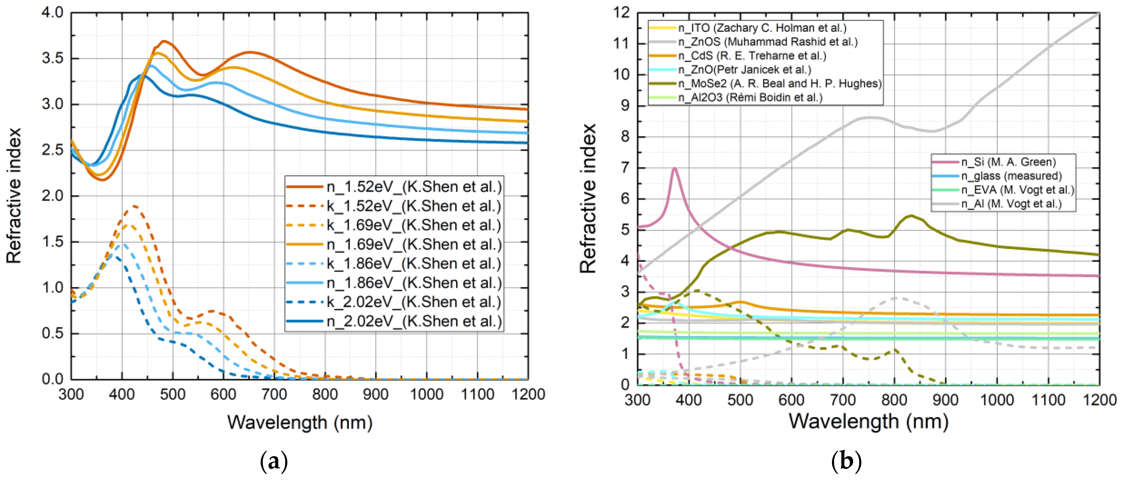
3.1. Data Used for the Simulations to Describe Materials
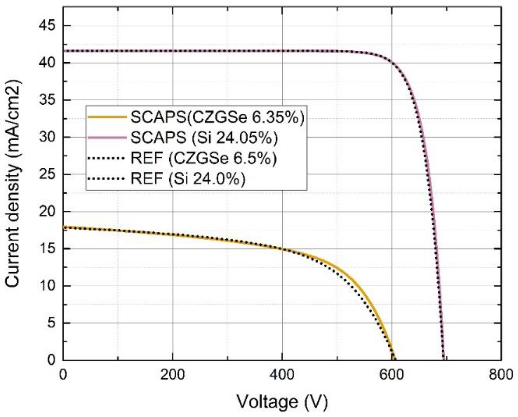
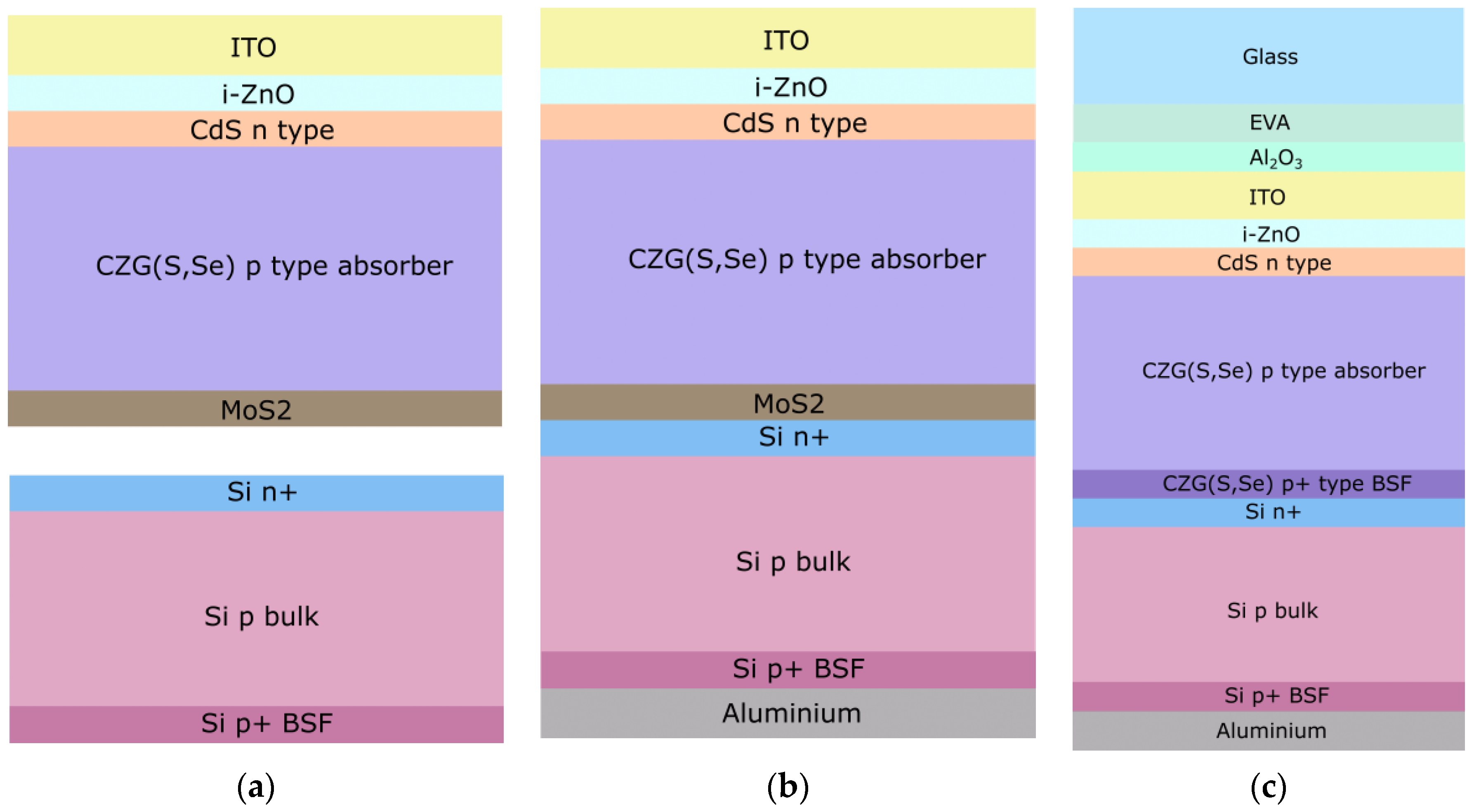
3.2. Reference Sub Cells for the CZG(S,Se)/Silicon Tandem Device
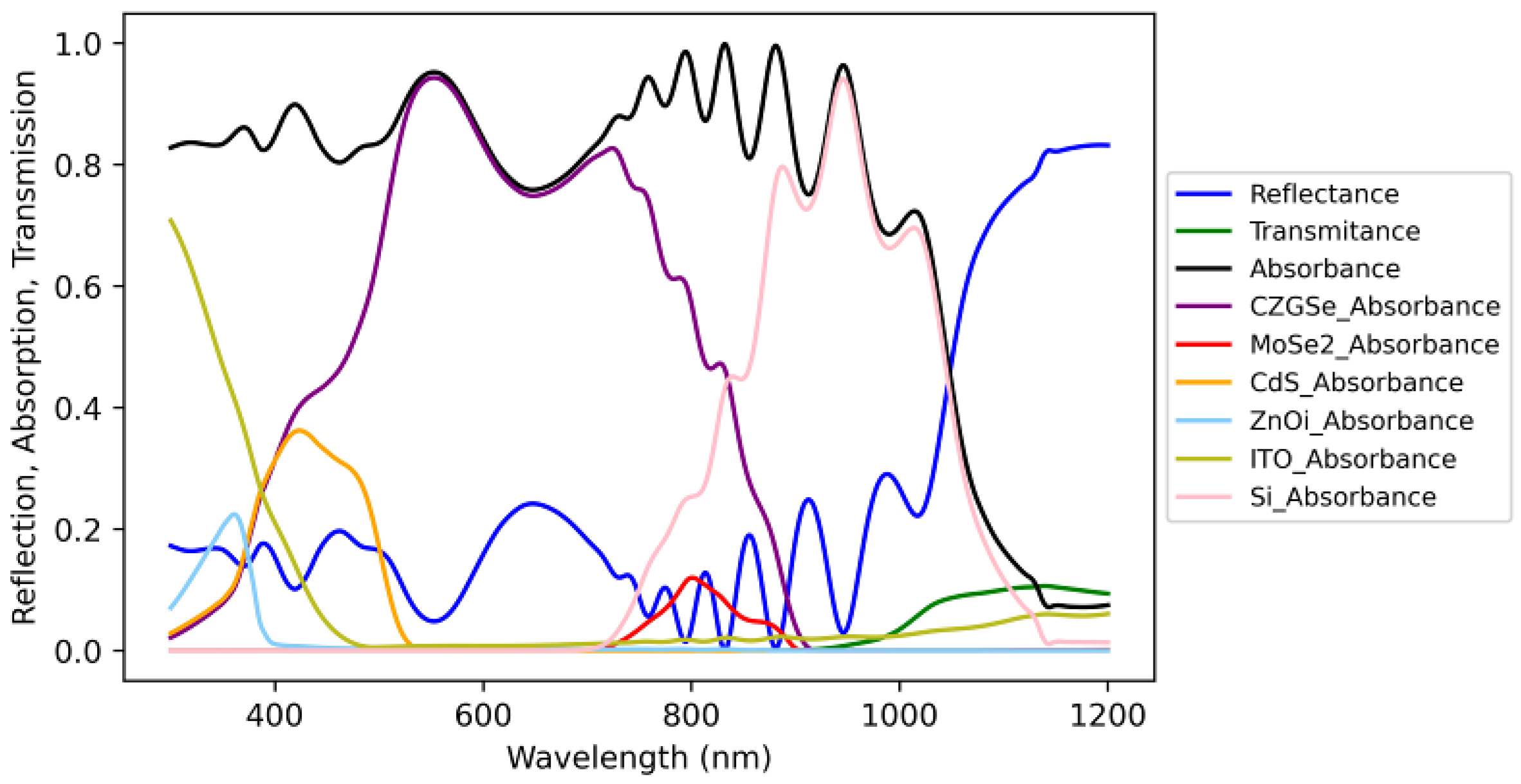
4. Results: Simulation Results Using Theoretical Refractive Index Data for Kesterite
- Encapsulation added (2 mm glass + 470 μm EVA);
- MoSe2 was removed to reduce parasitic absorption (due to the low bandgap of MoSe2) and the p+ back surface field (BSF) was added to the kesterite absorber;
- CdS was changed by ZnOS to reduce parasitic light absorption due to the low bandgap of CdS;
- CZGSe’s base doping increased from 1014 to 1016, according to S. Khelifi [14], and interface recombination velocity (at CdS/CZGSe interface) decreased from 105 to 103 cm/s;
- CZGSe’s effective carrier lifetime varied to observe its effect, and the requirements for obtaining an efficient tandem device;
- CZGSe thickness and band gap (by partial substitution of Se with S) were varied in order to see its effect and the requirements for obtaining an efficient tandem device;
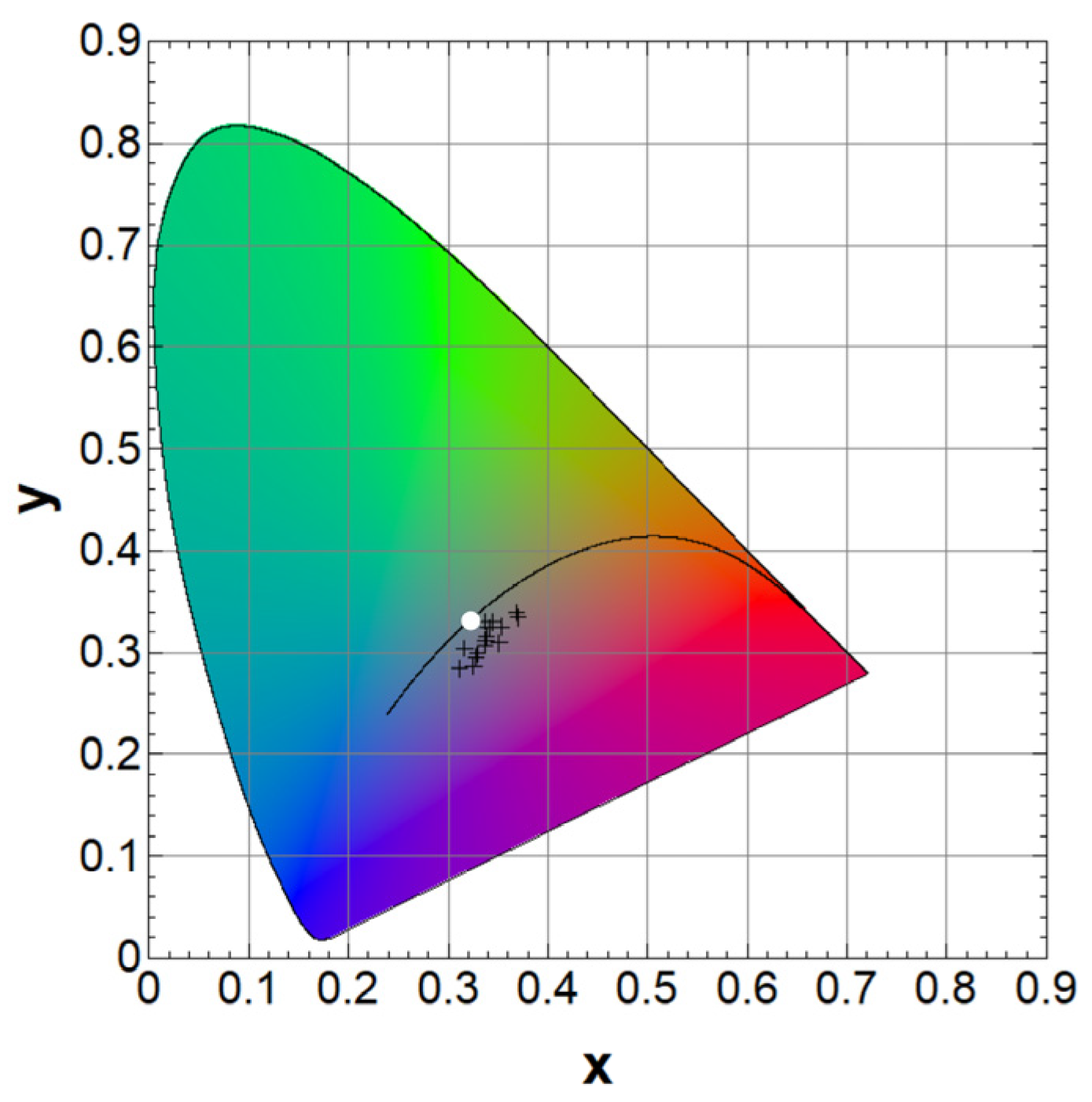
- An Al2O3 anti-reflective coating was added, and its thickness was optimized. The color effect on current matching and efficiency on the tandem device was observed.
4.1. REF Cells Connected in Series and Encapsulation Added
4.2. Mitigating Parasitic Loss and Carrier Recombination
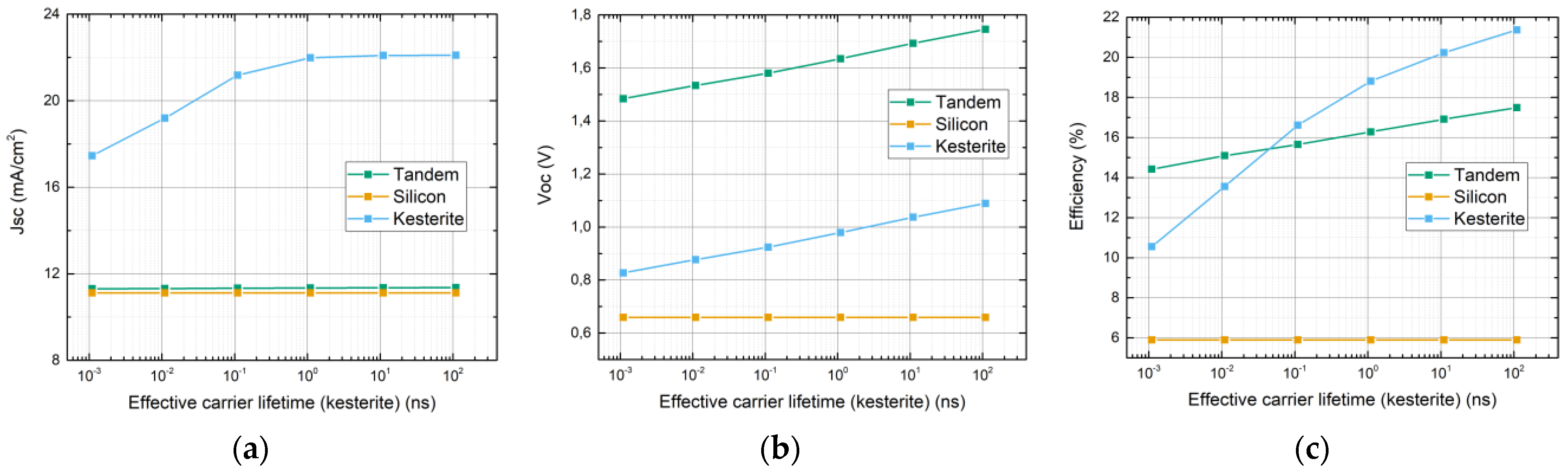
4.3. CZGSSe Crystal Quality Represented by Effective Carrier Lifetime
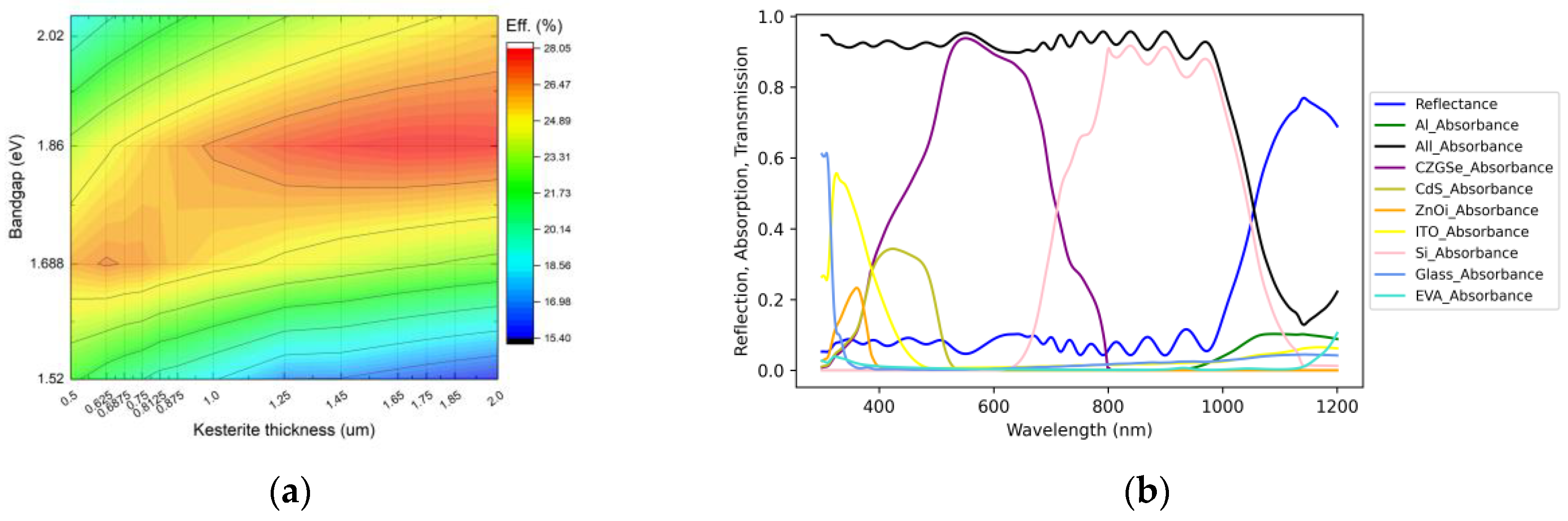
4.4. Effect of CZGSSe Thickness and Band Gap
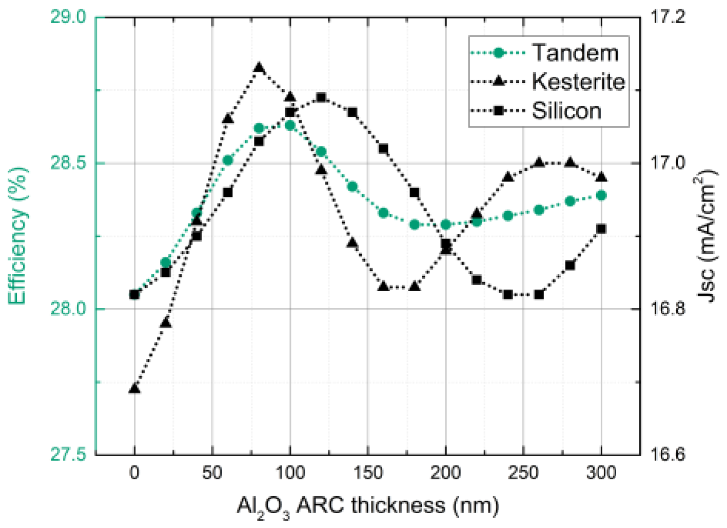
4.5. Al2O3 Anti-Reflective Coating Added and Its Thickness Optimized
5. Colorimetry and Tandem Viability for BIPV
6. Discussions
7. Conclusions
Author Contributions
Funding
Institutional Review Board Statement
Informed Consent Statement
Data Availability Statement
Conflicts of Interest
Appendix A
Appendix A.1. Calculations of Carrier Generation Profile
Appendix A.2. Calculation of Maximum Possible JSC and JSC Loss
Appendix B
Model for Effective Minority Carrier Lifetime and Interface Recombination Velocity
Appendix C
Additional Result Data

| Step | Reflectance | Glass | EVA | Al2O3 | ITO | ZnO-i | CdS | ZnOxS1−x | CZGSSe | MoSe2 | Si | Aluminum |
|---|---|---|---|---|---|---|---|---|---|---|---|---|
| 1 | 10.29 | - | - | - | 1.59 | 0.25 | 1.92 | - | 21.19 | 0.71 | 9.74 | 0.78 |
| 2 | 7.86 | 0.78 | 0.28 | - | 1.64 | 0.25 | 2.06 | - | 22.21 | 0.71 | 9.90 | 0.78 |
| 3 | 7.47 | 0.77 | 0.28 | - | 1.64 | 0.25 | 2.06 | - | 22.05 | - | 11.16 | 0.78 |
| 4 | 8.67 | 0.78 | 0.29 | - | 1.67 | 0.25 | - | 2.29 | 20.64 | - | 11.11 | 0.78 |
| 5 | 7.47 | 0.77 | 0.28 | - | 1.64 | 0.25 | 2.06 | - | 22.05 | - | 11.16 | 0.78 |
| 6 | 7.47 | 0.77 | 0.28 | - | 1.64 | 0.25 | 2.06 | - | 22.05 | - | 11.16 | 0.78 |
| 7 | 7.27 | 0.77 | 0.28 | - | 1.64 | 0.25 | 1.93 | - | 16.70 | - | 16.84 | 0.78 |
| 8 | 6.60 | 0.76 | 0.28 | 0.00 | 1.66 | 0.25 | 1.96 | - | 17.08 | - | 17.09 | 0.79 |

References
- Fawzy, S.; Osman, A.I.; Doran, J.; Rooney, D.W. Strategies for Mitigation of Climate Change: A Review. Environ. Chem. Lett. 2020, 18, 2069–2094. [Google Scholar] [CrossRef]
- Yoshikawa, K.; Kawasaki, H.; Yoshida, W.; Irie, T.; Konishi, K.; Nakano, K.; Uto, T.; Adachi, D.; Kanematsu, M.; Uzu, H.; et al. Silicon Heterojunction Solar Cell with Interdigitated Back Contacts for a Photoconversion Efficiency over 26%. Nat. Energy 2017, 2, 17032. [Google Scholar] [CrossRef]
- EPFL CSEM, EPFL Achieve 31.25% Efficiency for Tandem Perovskite-Silicon Solar Cell. Available online: https://www.pv-magazine.com/2022/07/07/csem-epfl-achieve-31-25-efficiency-for-tandem-perovskite-silicon-solar-cell/ (accessed on 3 September 2023).
- Green, M.A.; Dunlop, E.D.; Siefer, G.; Yoshita, M.; Kopidakis, N.; Bothe, K.; Hao, X. Solar Cell Efficiency Tables (Version 61). Prog. Photovolt. Res. Appl. 2023, 31, 3–16. [Google Scholar] [CrossRef]
- Oxford PV Oxford PV Sets New Solar Cell World Record. Available online: https://www.pv-magazine.com/2023/04/01/weekend-read-industry-and-researchers-in-tandem/ (accessed on 3 September 2023).
- Zhuang, J.; Wang, J.; Yan, F. Review on Chemical Stability of Lead Halide Perovskite Solar Cells; Springer Nature: Singapore, 2023; Volume 15, ISBN 4082002301046. [Google Scholar]
- The European Commission Communication from the Commission to the European ParliaMent. The Council, The European Economic and Social Committee and the Committee of the Regions on the 2017 List of Critical Raw Materials for the EU. Available online: https://eur-lex.europa.eu/legal-content/EN/ALL/?uri=COM:2017:0490:FIN (accessed on 25 May 2023).
- Schorr, S. Cation and Anion Mutations in Kesterites: A Way to Flexible Band Gap Energy Tuning. Sol. Energy Mater. Sol. Cells 2023, 249, 112044. [Google Scholar] [CrossRef]
- Zhou, J.; Xu, X.; Wu, H.; Wang, J.; Lou, L.; Yin, K.; Gong, Y.; Shi, J.; Luo, Y.; Li, D.; et al. Control of the Phase Evolution of Kesterite by Tuning of the Selenium Partial Pressure for Solar Cells with 13.8% Certified Efficiency. Nat. Energy 2023, 8, 526–535. [Google Scholar] [CrossRef]
- Wang, A.; He, M.; Green, M.A.; Sun, K.; Hao, X. A Critical Review on the Progress of Kesterite Solar Cells: Current Strategies and Insights. Adv. Energy Mater. 2023, 13, 2203046. [Google Scholar] [CrossRef]
- Giraldo, S.; Jehl, Z.; Placidi, M.; Izquierdo-Roca, V.; Pérez-Rodríguez, A.; Saucedo, E. Progress and Perspectives of Thin Film Kesterite Photovoltaic Technology: A Critical Review. Adv. Mater. 2019, 31, 1806692. [Google Scholar] [CrossRef]
- Mora-Herrera, D.; Pal, M.; Santos-Cruz, J. Theoretical Modelling and Device Structure Engineering of Kesterite Solar Cells to Boost the Conversion Efficiency over 20%. Sol. Energy 2021, 220, 316–330. [Google Scholar] [CrossRef]
- Jimenez-Arguijo, A.; Medaille, A.G.; Navarro-Güell, A.; Jimenez-Guerra, M.; Tiwari, K.J.; Placidi, M.; Mkehlane, M.S.; Iwuoha, E.; Perez-Rodriguez, A.; Saucedo, E.; et al. Setting the Baseline for the Modelling of Kesterite Solar Cells: The Case Study of Tandem Application. Sol. Energy Mater. Sol. Cells 2023, 251, 112109. [Google Scholar] [CrossRef]
- Khelifi, S.; Brammertz, G.; Choubrac, L.; Batuk, M.; Yang, S.; Meuris, M.; Barreau, N.; Hadermann, J.; Vrielinck, H.; Poelman, D.; et al. The Path towards Efficient Wide Band Gap Thin-Film Kesterite Solar Cells with Transparent Back Contact for Viable Tandem Application. Sol. Energy Mater. Sol. Cells 2021, 219, 110824. [Google Scholar] [CrossRef]
- Sivathanu, V.; Thangavel, R.; Lenka, T.R. Modeling and Performance Optimization of Two-Terminal Cu2ZnSnS4–Silicon Tandem Solar Cells. Int. J. Energy Res. 2021, 45, 10527–10537. [Google Scholar] [CrossRef]
- Vallisree, S.; Thangavel, R.; Lenka, T.R. Modelling, Simulation, Optimization of Si/ZnO and Si/ZnMgO Heterojunction Solar Cells. Mater. Res. Express 2019, 6, 025910. [Google Scholar] [CrossRef]
- Shen, K.; Jia, G.; Zhang, X.; Jiao, Z. The Electronic Structure, Elastic and Optical Properties of Cu2ZnGe(SexS1−x)4 Alloys: Density Functional Calculations. Mol. Phys. 2016, 114, 2948–2957. [Google Scholar] [CrossRef]
- Unold, T. Accelerating Research on Novel Photovoltaic Materials. Faraday Discuss. 2022, 239, 235–249. [Google Scholar] [CrossRef] [PubMed]
- Hille, S.L.; Curtius, H.C.; Wüstenhagen, R. Red Is the New Blue—The Role of Color, Building Integration and Country-of-Origin in Homeowners’ Preferences for Residential Photovoltaics. Energy Build. 2018, 162, 21–31. [Google Scholar] [CrossRef]
- Burgelman, M.; Decock, K.; Khelifi, S.; Abass, A. Advanced Electrical Simulation of Thin Film Solar Cells. Thin Solid Film 2013, 535, 296–301. [Google Scholar] [CrossRef]
- Byrnes, S.J. Multilayer Optical Calculations. arXiv 2016, arXiv:1603.02720. [Google Scholar]
- Macleod, H.A. Thin Film Optical Filters, 5th ed.; Brown, R.G.W., Pike, E.R., Eds.; CRC Press Taylor & Francis Group: Boca Raton, FL, USA, 2018; ISBN 9781138198241. [Google Scholar]
- Valiei, M.; Shaibani, P.M.; Abdizadeh, H.; Kolahdouz, M.; Asl Soleimani, E.; Poursafar, J. Design and Optimization of Single, Double and Multilayer Anti-Reflection Coatings on Planar and Textured Surface of Silicon Solar Cells. Mater. Today Commun. 2022, 32, 104144. [Google Scholar] [CrossRef]
- Haque, M.D.; Ali, M.H.; Rahman, M.F.; Islam, A.Z.M.T. Numerical Analysis for the Efficiency Enhancement of MoS2 Solar Cell: A Simulation Approach by SCAP-1D. Opt. Mater. 2022, 131, 112678. [Google Scholar] [CrossRef]
- Rashid, M.; Noor, N.A.; Sabir, B.; Ali, S.; Sajjad, M.; Hussain, F.; Khan, N.U.; Amin, B.; Khenata, R. Ab-Initio Study of Fundamental Properties of Ternary ZnO1−XSx Alloys by Using Special Quasi-Random Structures. Comput. Mater. Sci. 2014, 91, 285–291. [Google Scholar] [CrossRef]
- Jafarzadeh, F.; Aghili, H.; Nikbakht, H.; Javadpour, S. Design and Optimization of Highly Efficient Perovskite/Homojunction SnS Tandem Solar Cells Using SCAPS-1D. Sol. Energy 2022, 236, 195–205. [Google Scholar] [CrossRef]
- Holman, Z.C.; Filipič, M.; Descoeudres, A.; De Wolf, S.; Smole, F.; Topič, M.; Ballif, C. Infrared Light Management in High-Efficiency Silicon Heterojunction and Rear-Passivated Solar Cells. J. Appl. Phys. 2013, 113, 013107. [Google Scholar] [CrossRef]
- Yu, S.Y.; Hassan, M.A.; Johar, M.A.; Ryu, S.W. Optical and Structural Analysis of Zinc Oxysulfide Digital Alloys Grown by Atomic Layer Deposition. J. Korean Phys. Soc. 2018, 73, 649–655. [Google Scholar] [CrossRef]
- Treharne, R.E.; Seymour-Pierce, A.; Durose, K.; Hutchings, K.; Roncallo, S.; Lane, D. Optical Design and Fabrication of Fully Sputtered CdTe/CdS Solar Cells. J. Phys. Conf. Ser. 2011, 286, 012038. [Google Scholar] [CrossRef]
- Aguilar, O.; de Castro, S.; Godoy, M.P.F.; Rebello Sousa Dias, M. Optoelectronic Characterization of Zn1−xCdxO Thin Films as an Alternative to Photonic Crystals in Organic Solar Cells. Opt. Mater. Express 2019, 9, 3638. [Google Scholar] [CrossRef]
- Beal, A.R.; Hughes, H.P. Kramers-Kronig Analysis of the Reflectivity Spectra of 2H-MoS2, 2H-MoSe2 and 2H-MoTe2. J. Phys. C Solid State Phys. 1979, 12, 881. [Google Scholar] [CrossRef]
- Green, M.A. Improved Silicon Optical Parameters at 25 °C, 295 K and 300 K Including Temperature Coefficients. Prog. Photovolt. Res. Appl. 2022, 30, 164–179. [Google Scholar] [CrossRef]
- Vogt, M.R.; Holst, H.; Schulte-Huxel, H.; Blankemeyer, S.; Witteck, R.; Hinken, D.; Winter, M.; Min, B.; Schinke, C.; Ahrens, I.; et al. Optical Constants of UV Transparent EVA and the Impact on the PV Module Output Power under Realistic Irradiation. Energy Procedia 2016, 92, 523–530. [Google Scholar] [CrossRef]
- Boidin, R.; Halenkovič, T.; Nazabal, V.; Beneš, L.; Němec, P. Pulsed Laser Deposited Alumina Thin Films. Ceram. Int. 2016, 42, 1177–1182. [Google Scholar] [CrossRef]
- Palik, E.D. Handbook of Optical Constants of Solids; Elsevier Inc.: Amsterdam, The Netherlands, 2012; Volume 1, ISBN 9780080547213. [Google Scholar]
- Anefnaf, I.; Aazou, S.; Sánchez, Y.; Vidal-Fuentes, P.; Fonoll-Rubio, R.; Tiwari, K.J.; Giraldo, S.; Li-Kao, Z.J.; Andrade-Arvizu, J.; Guc, M.; et al. Insights on the Limiting Factors of Cu2ZnGeSe4 Based Solar Cells. Sol. Energy Mater. Sol. Cells 2021, 227, 111106. [Google Scholar] [CrossRef]
- Green, M.A.; Dunlop, E.D.; Hohl-Ebinger, J.; Yoshita, M.; Kopidakis, N.; Bothe, K.; Hinken, D.; Rauer, M.; Hao, X. Solar Cell Efficiency Tables (Version 60). Prog. Photovolt. Res. Appl. 2022, 30, 687–701. [Google Scholar] [CrossRef]
- Ballif, C.; Haug, F.J.; Boccard, M.; Verlinden, P.J.; Hahn, G. Status and Perspectives of Crystalline Silicon Photovoltaics in Research and Industry. Nat. Rev. Mater. 2022, 7, 597–616. [Google Scholar] [CrossRef]
- Lee, Y.S.; Gershon, T.; Gunawan, O.; Todorov, T.K.; Gokmen, T.; Virgus, Y.; Guha, S. Cu2ZnSnSe4 Thin-Film Solar Cells by Thermal Co-Evaporation with 11.6% Efficiency and Improved Minority Carrier Diffusion Length. Adv. Energy Mater. 2015, 5, 2–5. [Google Scholar] [CrossRef]
- Gokmen, T.; Gunawan, O.; Todorov, T.K.; Mitzi, D.B. Band Tailing and Efficiency Limitation in Kesterite Solar Cells. Appl. Phys. Lett. 2013, 103, 103506. [Google Scholar] [CrossRef]
- Repins, I.L.; Moutinho, H.; Choi, S.G.; Kanevce, A.; Kuciauskas, D.; Dippo, P.; Beall, C.L.; Carapella, J.; Dehart, C.; Huang, B.; et al. Indications of Short Minority-Carrier Lifetime in Kesterite Solar Cells. J. Appl. Phys. 2013, 114, 084507. [Google Scholar] [CrossRef]
- Zeng, L.; Li, M.; Chen, Y.; Shen, H. A Simplified Method to Modulate Colors on Industrial Multicrystalline Silicon Solar Cells with Reduced Current Losses. Sol. Energy 2014, 103, 343–349. [Google Scholar] [CrossRef]
- Rudzikas, M.; Šetkus, A.; Stange, M.; Ulbikas, J.; Ulyashin, A. Simple Interference Based Colorization of Si Based Solar Cells and Panels with ITO/SiNx:H Double Layer Antireflective Coatings. Sol. Energy 2020, 207, 218–227. [Google Scholar] [CrossRef]
- Tobías, I.; El Moussaoui, A.; Luque, A. Colored Solar Cells with Minimal Current Mismatch. IEEE Trans. Electron Devices 1999, 46, 1858–1865. [Google Scholar] [CrossRef]
- León, M.; Levcenko, S.; Serna, R.; Gurieva, G.; Nateprov, A.; Merino, J.M.; Friedrich, E.J.; Fillat, U.; Schorr, S.; Arushanov, E. Optical Constants of Cu2ZnGeS4 Bulk Crystals. J. Appl. Phys. 2010, 108, 093502. [Google Scholar] [CrossRef]
- León, M.; Levcenko, S.; Serna, R.; Nateprov, A.; Gurieva, G.; Merino, J.M.; Schorr, S.; Arushanov, E. Spectroscopic Ellipsometry Study of Cu2ZnGeSe4 and Cu2ZnSiSe4 Poly-Crystals. Mater. Chem. Phys. 2013, 141, 58–62. [Google Scholar] [CrossRef]
- Chen, S.; Gong, X.G.; Walsh, A.; Wei, S.H. Electronic Structure and Stability of Quaternary Chalcogenide Semiconductors Derived from Cation Cross-Substitution of II-VI and I-III-VI2 Compounds. Phys. Rev. B Condens. Matter Mater. Phys. 2009, 79, 165211. [Google Scholar] [CrossRef]
- Todorov, T.; Gunawan, O.; Guha, S. A Road towards 25% Efficiency and beyond: Perovskite Tandem Solar Cells. Mol. Syst. Des. Eng. 2016, 1, 370–376. [Google Scholar] [CrossRef]
- Luque, A.; Hegedus, S. Handbook of Photovoltaic Science and Engineering; John Wiley & Sons: Hoboken, NJ, USA, 2011; ISBN 9780470721698. [Google Scholar]
- NREL. Reference Air Mass 1.5 Spectra. Available online: https://www.nrel.gov/grid/solar-resource/assets/data/astmg173.xls (accessed on 3 September 2023).


| Parameter | MoSe2 [24] | CZGSe [14] | CdS [14] | ZnO0.2S0.8 [25] | ZnO [14] | ITO [26] | Si (Bulk) [13] |
|---|---|---|---|---|---|---|---|
| d (μm) | 0.02 | 1.45 | 0.050 | 0.050 | 0.050 | 0.200 | 200 |
| Eg (eV) | 1.29 | 1.5 | 2.4 | 3.07 [12] | 3.3 | 3.65 | 1.12 |
| χ (eV) | 4.2 | 4.41 ** | 4.2 | 4.3 [12] | 4.4 | 4.8 | 4.5 |
| ε (relative) | 13.6 | 6.950 [12] | 8.28 [12] | 9 | 7.8 [12] | 8.9 | 11.9 |
| μn (cm2/V∙s) | 100 | 100 | 100 | 100 | 100 | 10 | 150 |
| μp (cm2/V∙s) | 25 | 20 | 25 | 25 | 25 | 10 | 45 |
| Nd (cm−3) | - | - | 1017 | 3.93 × 10¹⁸ | 1018 | 1019 | - |
| Na (cm−3) | 2.25 × 10¹⁵ * | 1014 * | - | - | - | 3 × 10¹⁵ | |
| CB effective density of states (1/cm3) | 2.2 × 10¹⁸ | 1.9 × 10¹⁸ | 3.1 × 10¹⁸ | 2.2 × 10¹⁸ | 3.6 × 10¹⁸ | 5.2 × 10¹⁸ | 2.8 × 10¹⁹ |
| VB effective density of states (1/cm3) | 1.8 × 10¹⁹ | 1.5 × 10¹⁹ | 1.4 × 10¹⁹ | 1.8 × 10¹⁹ | 1.1 × 10¹⁹ | 1.8 × 10¹⁸ | 1.04 × 10¹⁹ |
| electron thermal velocity (cm/s) | 2.2 × 10⁷ | (2.7 × 10⁷) [12] | (2.3 × 10⁷) [12] | 107 | (2.2 × 10⁷) [12] | 107 | 107 |
| hole thermal velocity (cm/s) | 1.5 × 10⁷ | (1.3 × 10⁷) [12] | (1.4 × 10⁷) [12] | 107 | (1.5 × 10⁷) [12] | 107 | 107 |
| JSC, mA/cm2 | VOC, mV | Efficiency, % | FF, % | τ, s * | Source: | |
|---|---|---|---|---|---|---|
| REF CZGSe cell | 17.8 | 606 | 6.5 | 60 | ? ** | I. Anefnaf et al. [36] |
| My REF CZGSe cell SCAPS | 17.92 | 606 | 6.35 | 58.51 | 1.1 × 10⁻¹¹ | |
| REF silicon cell *** | 41.58 | 694 | 24.0 | 83.3 | ? ** | M. Green [37] |
| My REF silicon cell SCAPS | 41.50 | 694.3 | 23.97 | 83.2 | 1 × 10⁻³ **** |
| Step | CZGSSe | Silicon | Tandem | |||||||||
|---|---|---|---|---|---|---|---|---|---|---|---|---|
| VOC, V | JSC, mA/cm2 | Eff, % | FF, % | VOC, V | JSC, mA/cm2 | Eff, % | FF, % | VOC, V | JSC, mA/cm2 | Eff, % | FF, % | |
| 0 | 0.606 | 17.56 | 6.17 | 58.0 | 0.655 | 9.7 | 5.14 | 80.91 | 1.259 | 9.83 | 10.21 | 82.54 |
| 1 | 0.608 | 18.38 | 6.46 | 57.8 | 0.655 | 9.86 | 5.22 | 80.97 | 1.26 | 9.99 | 10.41 | 82.71 |
| 2 | 0.842 | 19.74 | 11.44 | 68.82 | 0.659 | 11.12 | 5.9 | 80.62 | 1.499 | 11.31 | 14.6 | 86.1 |
| 3 | 0.842 | 18.38 | 10.61 | 68.6 | 0.659 | 11.07 | 5.88 | 80.6 | 1.497 | 11.26 | 14.46 | 85.77 |
| 4 | 0.877 | 19.19 | 13.56 | 80.61 | 0.659 | 11.12 | 5.9 | 80.62 | 1.534 | 11.32 | 15.09 | 86.92 |
| 5 | 1.037 | 22.09 | 20.23 | 88.34 | 0.659 | 11.12 | 5.9 | 80.62 | 1.693 | 11.35 | 16.91 | 88.0 |
| 6 | 1.293 | 16.69 | 19.09 | 88.49 | 0.671 | 16.82 | 8.97 | 79.47 | 1.959 | 16.75 | 28.05 | 85.47 |
| 7 | 1.293 | 17.09 | 19.56 | 88.54 | 0.671 | 17.07 | 9.11 | 79.52 | 1.961 | 17.32 | 28.63 | 84.3 |
Disclaimer/Publisher’s Note: The statements, opinions and data contained in all publications are solely those of the individual author(s) and contributor(s) and not of MDPI and/or the editor(s). MDPI and/or the editor(s) disclaim responsibility for any injury to people or property resulting from any ideas, methods, instructions or products referred to in the content. |
© 2023 by the authors. Licensee MDPI, Basel, Switzerland. This article is an open access article distributed under the terms and conditions of the Creative Commons Attribution (CC BY) license (https://creativecommons.org/licenses/by/4.0/).
Share and Cite
Rudzikas, M.; Pakalka, S.; Donėlienė, J.; Šetkus, A. Exploring the Potential of Pure Germanium Kesterite for a 2T Kesterite/Silicon Tandem Solar Cell: A Simulation Study. Materials 2023, 16, 6107. https://doi.org/10.3390/ma16186107
Rudzikas M, Pakalka S, Donėlienė J, Šetkus A. Exploring the Potential of Pure Germanium Kesterite for a 2T Kesterite/Silicon Tandem Solar Cell: A Simulation Study. Materials. 2023; 16(18):6107. https://doi.org/10.3390/ma16186107
Chicago/Turabian StyleRudzikas, Matas, Saulius Pakalka, Jolanta Donėlienė, and Arūnas Šetkus. 2023. "Exploring the Potential of Pure Germanium Kesterite for a 2T Kesterite/Silicon Tandem Solar Cell: A Simulation Study" Materials 16, no. 18: 6107. https://doi.org/10.3390/ma16186107
APA StyleRudzikas, M., Pakalka, S., Donėlienė, J., & Šetkus, A. (2023). Exploring the Potential of Pure Germanium Kesterite for a 2T Kesterite/Silicon Tandem Solar Cell: A Simulation Study. Materials, 16(18), 6107. https://doi.org/10.3390/ma16186107