
Charge Trapping and Emission Properties in CAAC-IGZO Transistor: A First-Principles Calculations

 and
and 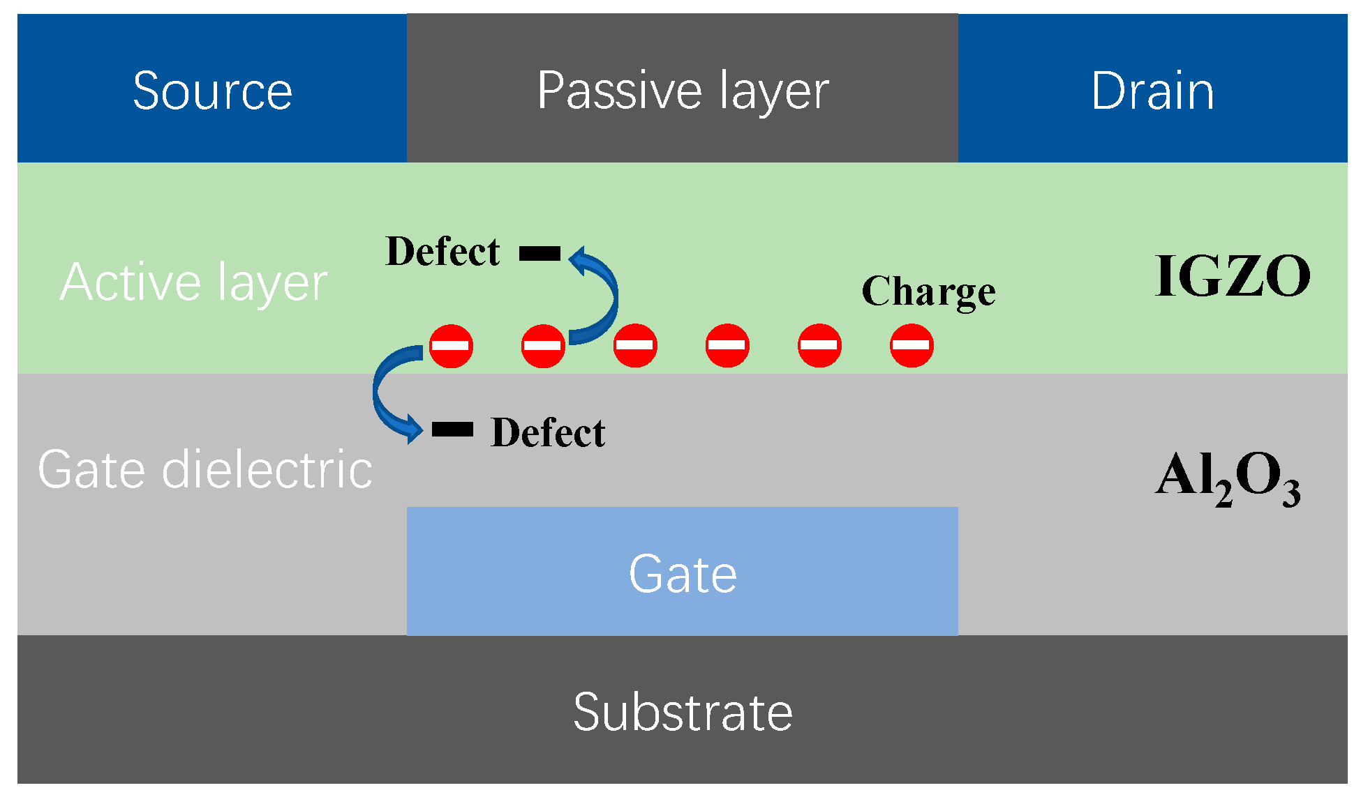
Abstract
1. Introduction
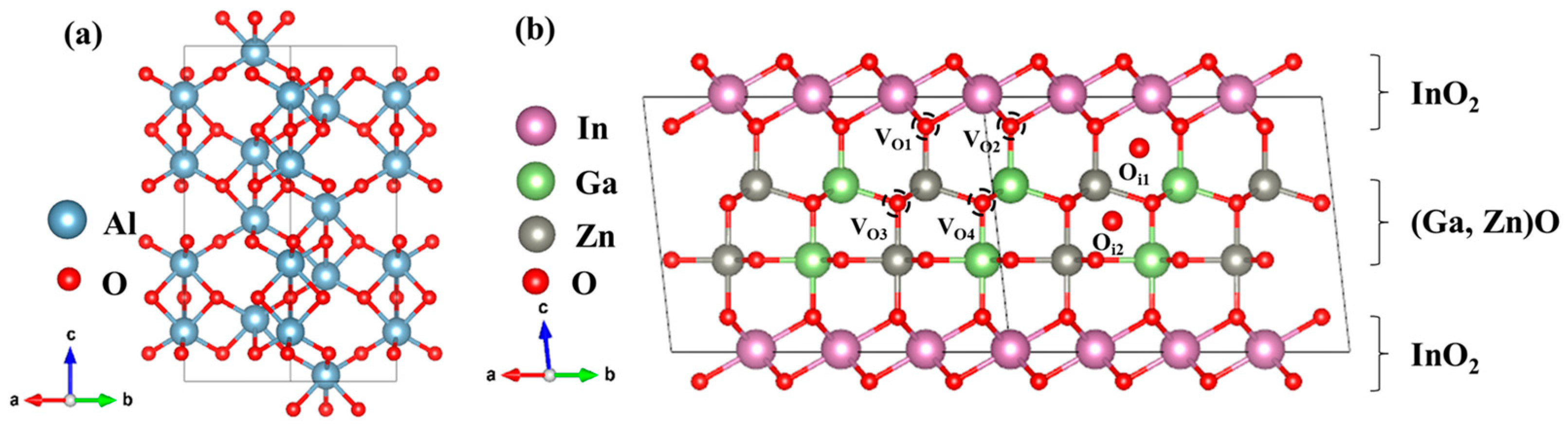
2. Computation Methodology
3. Result and Discussion
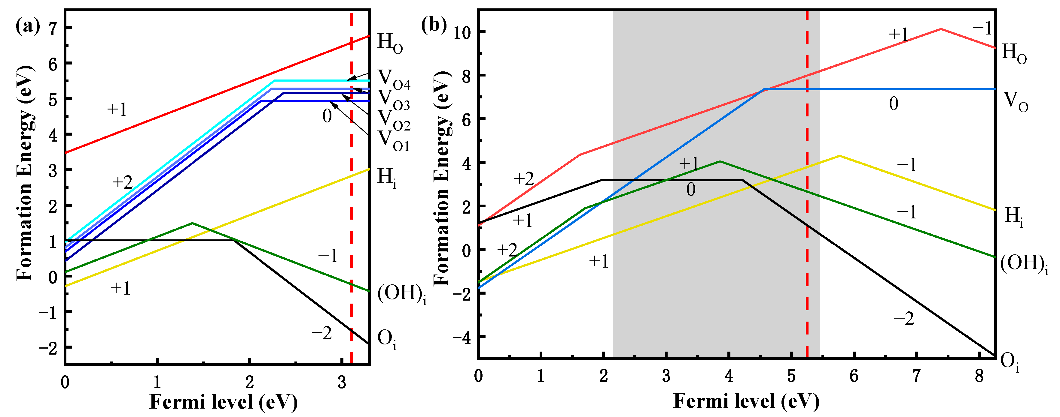
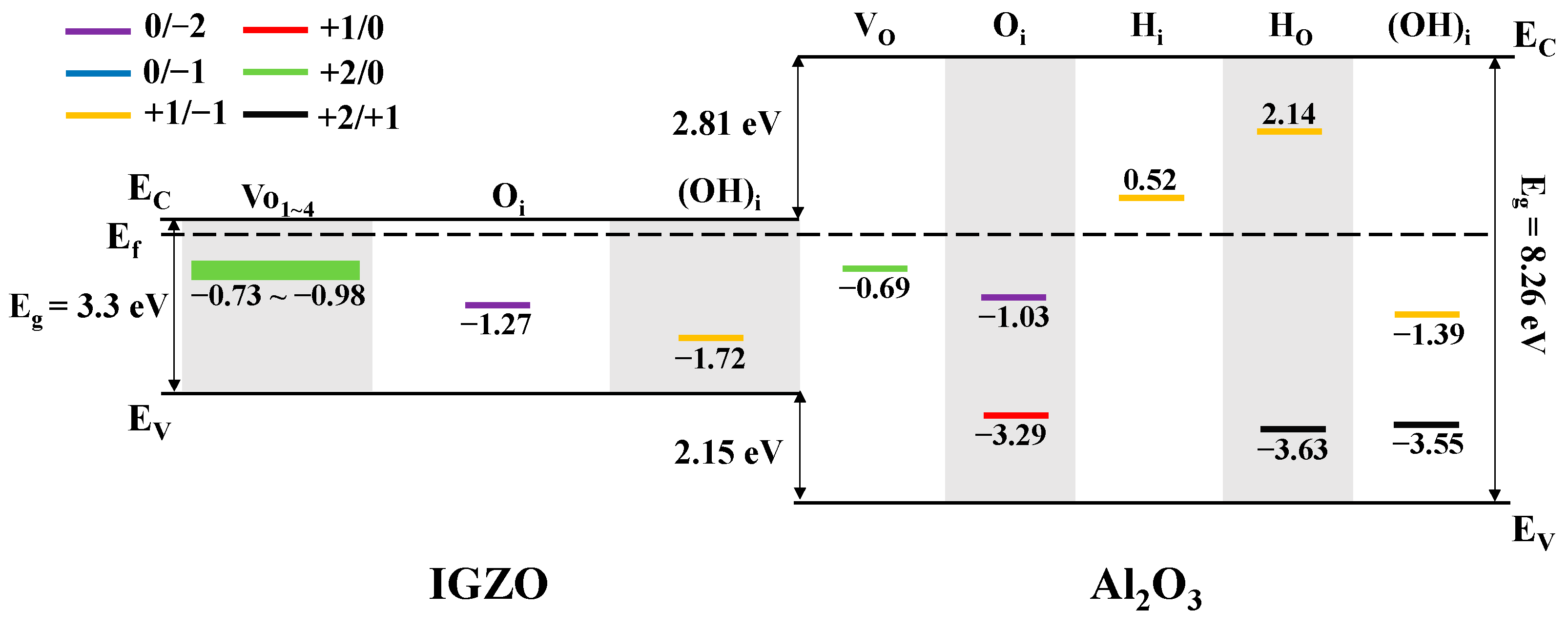
3.1. Formation Energy and Transition Level
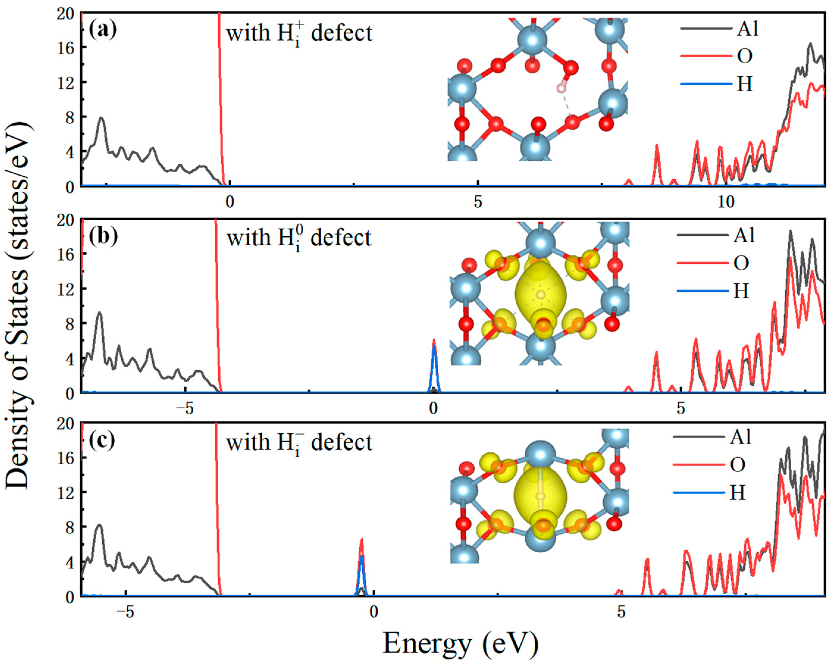
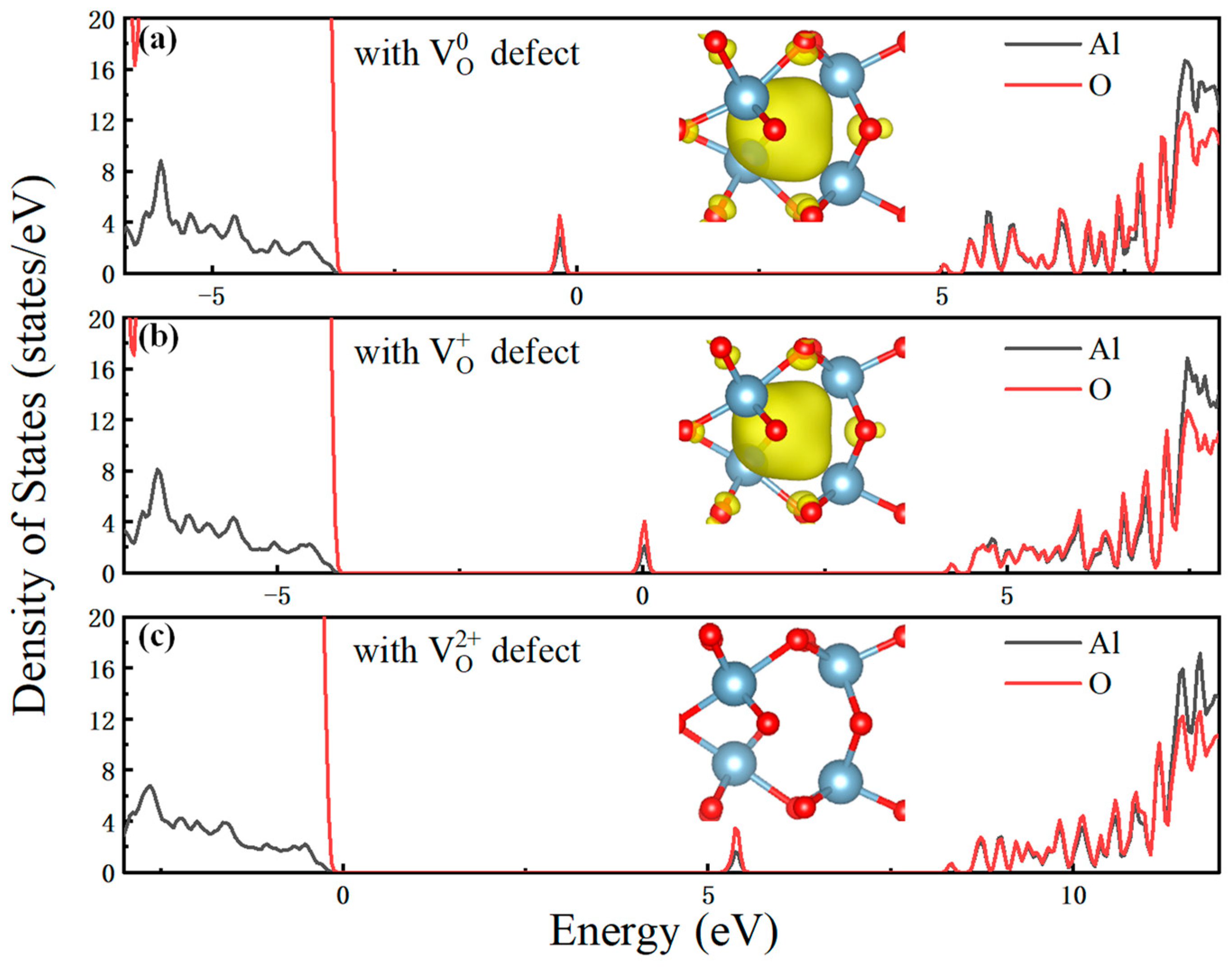
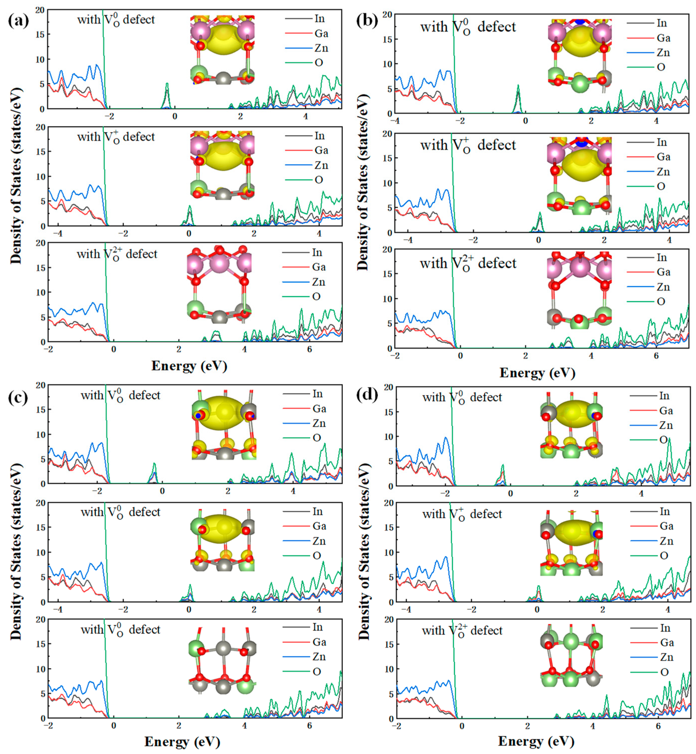
3.2. Electronic Properties of Charge Capture/Emission Process
3.3. Kinetics of Charge Capture/Emission Process
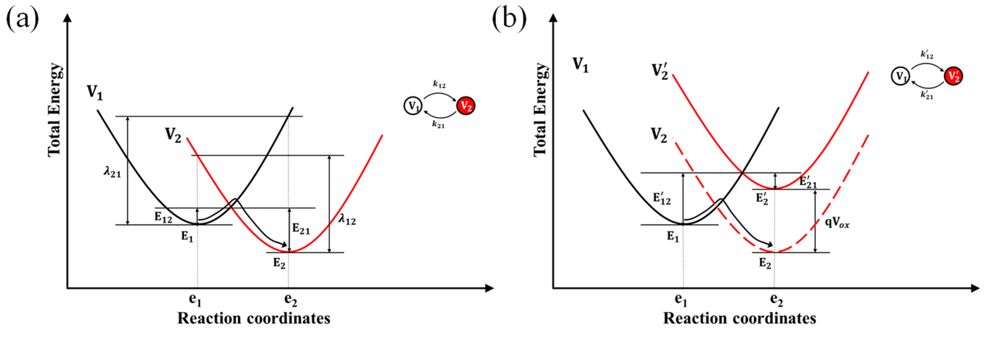
3.3.1. Nonradiative Multiphonon Transition Process
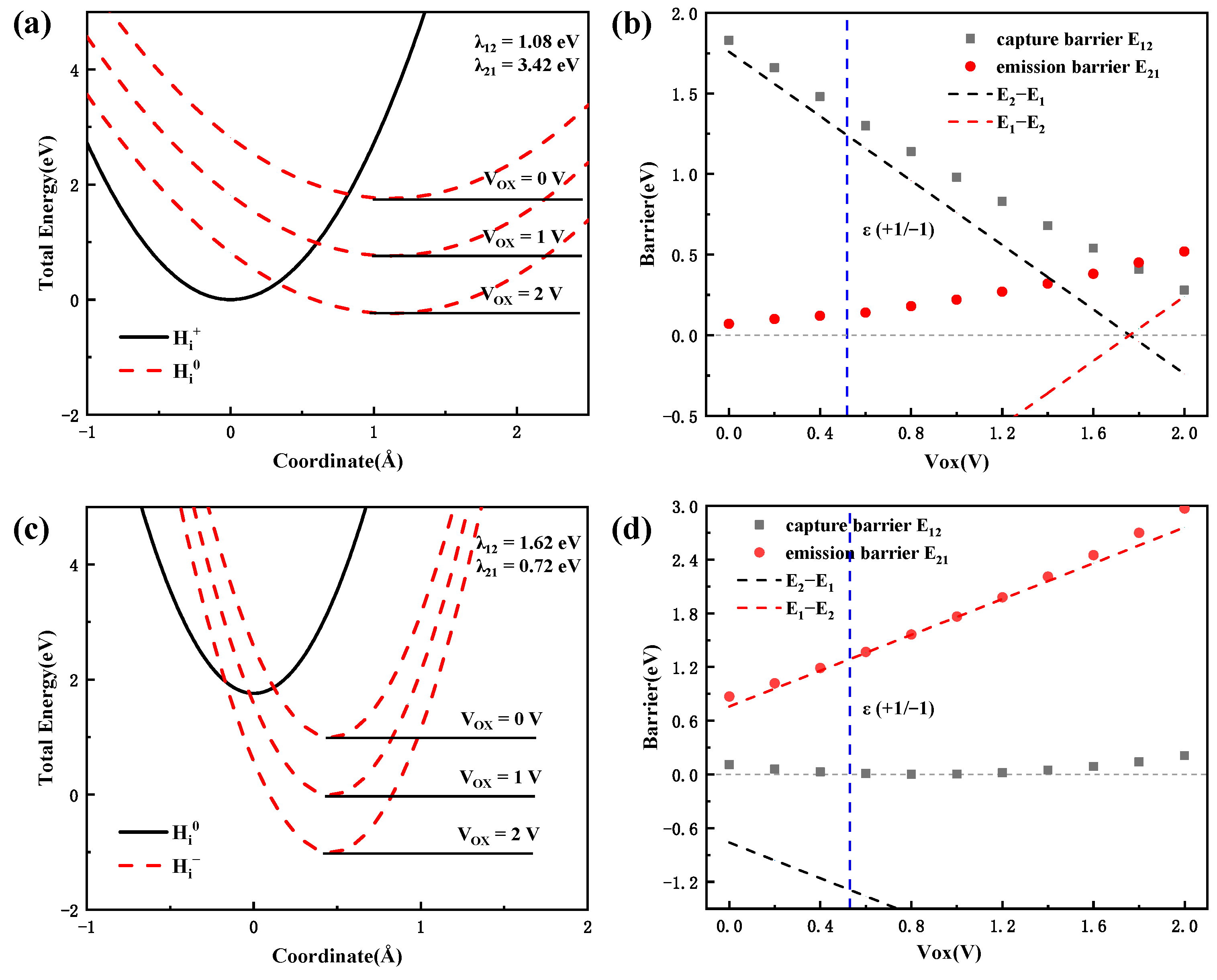
3.3.2. Charge Transition Process in Al2O3
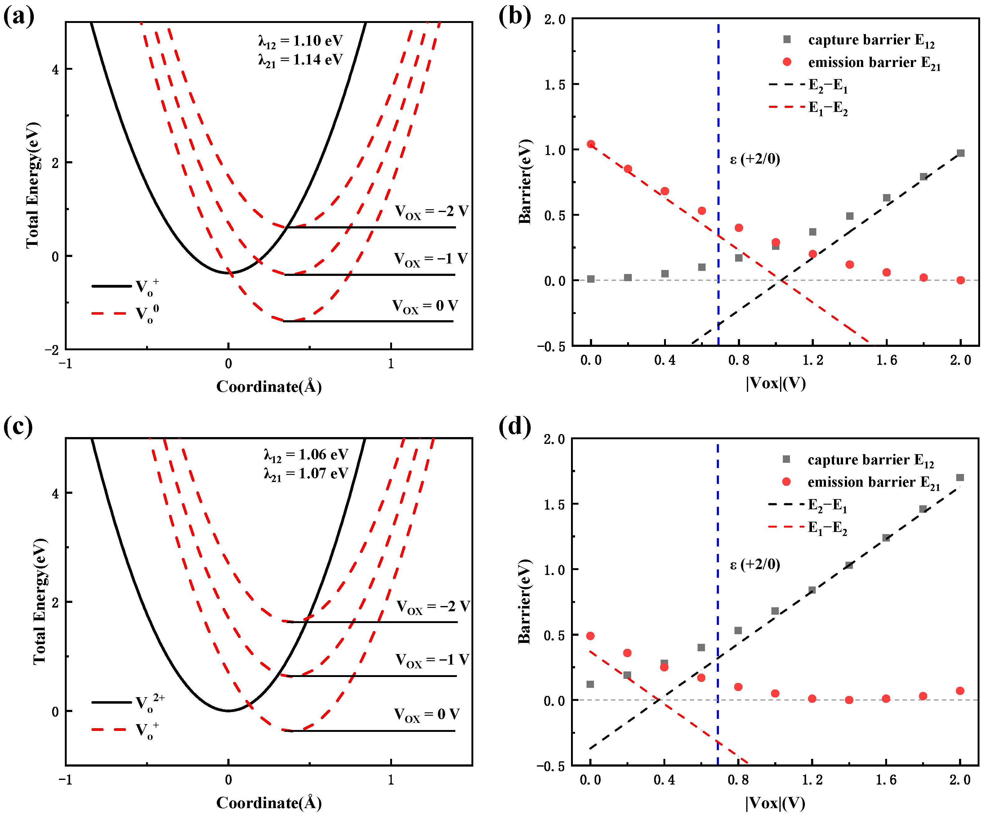
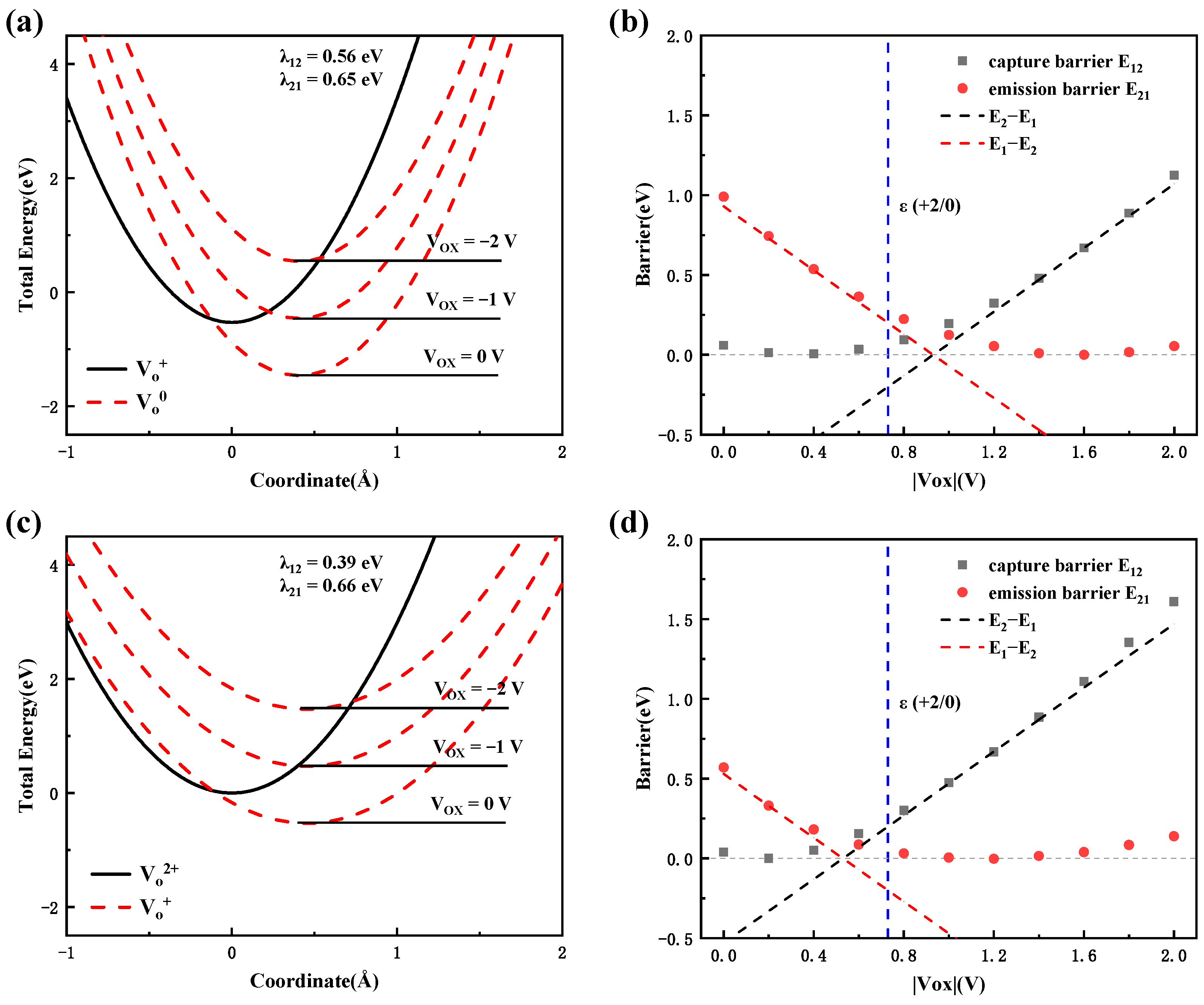
3.3.3. Charge Transition Process in CAAC-IGZO
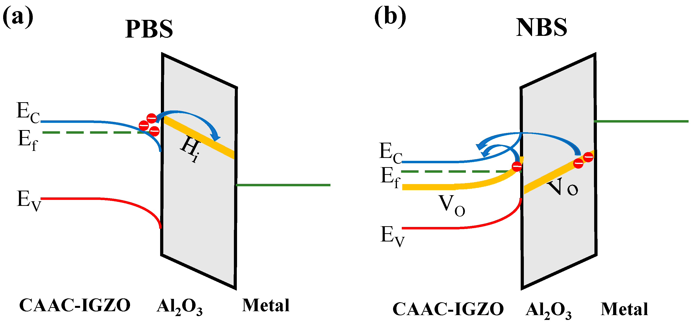
3.4. Instability Effects in IGZO Device Induced by Charge Capture/emission Process
4. Conclusions
Author Contributions
Funding
Institutional Review Board Statement
Informed Consent Statement
Data Availability Statement
Acknowledgments
Conflicts of Interest
References
- Nomura, K.; Ohta, H.; Takagi, A.; Kamiya, T.; Hirano, M.; Hosono, H. Room-temperature fabrication of transparent flexible thin-film transistors using amorphous oxide semiconductors. Nature 2004, 432, 488–492. [Google Scholar] [CrossRef] [PubMed]
- Kamiya, T.; Nomura, K.; Hosono, H. Present status of amorphous In-Ga-Zn-O thin-film transistors. Sci. Technol. Adv. Mater. 2010, 11, 044305. [Google Scholar] [CrossRef] [PubMed]
- Wager, J.F.; Yeh, B.; Hoffman, R.L.; Keszler, D.A. An amorphous oxide semiconductor thin-film transistor route to oxide electronics. Curr. Opin. Solid State Mater. Sci. 2014, 18, 53–61. [Google Scholar] [CrossRef]
- Jeong, J.K. The status and perspectives of metal oxide thin-film transistors for active matrix flexible displays. Semicond. Sci. Technol. 2011, 26, 034008. [Google Scholar] [CrossRef]
- Hsu, C.M.; Tzou, W.C.; Yang, C.F.; Liou, Y.J. Investigation of the High Mobility IGZO Thin Films by Using Co-Sputtering Method. Materials 2015, 8, 2769–2781. [Google Scholar] [CrossRef]
- Kato, K.; Shionoiri, Y.; Sekine, Y.; Furutani, K.; Hatano, T.; Aoki, T.; Sasaki, M.; Tomatsu, H.; Koyama, J.; Yamazaki, S. Evaluation of Off-State Current Characteristics of Transistor Using Oxide Semiconductor Material, Indium-Gallium-Zinc Oxide. Jpn. J. Appl. Phys. 2012, 51, 021201. [Google Scholar] [CrossRef]
- Oota, M.; Ando, Y.; Tsuda, K.; Koshida, T.; Oshita, S.; Suzuki, A.; Fukushima, K.; Nagatsuka, S.; Onuki, T.; Hodo, R.; et al. 3D-Stacked CAAC-In-Ga-Zn Oxide FETs with Gate Length of 72 nm. In Proceedings of the 65th IEEE Annual International Electron Devices Meeting (IEDM), San Francisco, CA, USA, 9–11 December 2019. [Google Scholar]
- Kunitake, H.; Ohshima, K.; Tsuda, K.; Matsumoto, N.; Sawai, H.; Yanagisawa, Y.; Saga, S.; Arasawa, R.; Seki, T.; Tokumaru, R.; et al. High thermal tolerance of 25-nm c-axis aligned crystalline In-Ga-Zn oxide FET. In Proceedings of the 64th IEEE Annual International Electron Devices Meeting (IEDM), San Francisco, CA, USA, 1–5 December 2018. [Google Scholar]
- Samanta, S.; Han, K.Z.; Sun, C.; Wang, C.K.; Thean, A.V.Y.; Gong, X. Amorphous IGZO TFTs featuring Extremely-Scaled Channel Thickness and 38 nm Channel Length: Achieving Record High G(m,max) of 125 µS/µm at V-DS of 1 V and I-ON ( ) of 350 µA/µm. In Proceedings of the IEEE Symposium on VLSI Technology and Circuits, Electr Network, Honolulu, HI, USA, 15–19 June 2020. [Google Scholar]
- Sheng, J.; Hong, T.; Lee, H.M.; Kim, K.; Sasase, M.; Kim, J.; Hosono, H.; Park, J.S. Amorphous IGZO TFT with High Mobility of similar to 70 cm(2)/(V s) via Vertical Dimension Control Using PEALD. ACS Appl. Mater. Interfaces 2019, 11, 40300–40309. [Google Scholar] [CrossRef]
- Saito, N.; Sawabe, T.; Kataoka, J.; Ueda, T.; Tezuka, T.; Ikeda, K. High mobility (>30 cm2V−1s−1) and low source/drain parasitic resistance In-Zn-O BEOL transistor with ultralow <10–20 A µm−1 off-state leakage current. Jpn. J. Appl. Phys. 2019, 58, SBBJ07. [Google Scholar] [CrossRef]
- Belmonte, A.; Oh, H.; Rassoul, N.; Donadio, G.L.; Mitard, J.; Dekkers, H.; Delhougne, R.; Subhechha, S.; Chasin, A.; van Setten, M.J.; et al. Capacitor-less, Long-Retention (>400 s) DRAM Cell Paving the Way towards Low-Power and High-Density Monolithic 3D DRAM. In Proceedings of the IEEE International Electron Devices Meeting (IEDM), Electr Network, San Francisco, CA, USA, 12–18 December 2020. [Google Scholar]
- Shunpei Yamazaki, M.F. Physics and Technology of Crystalline Oxide Semiconductor CAAC-IGZO: Application to LSI; Wiley Publishing: Hoboken, NJ, USA, 2016. [Google Scholar]
- Nomura, K.; Kamiya, T.; Kikuchi, Y.; Hirano, M.; Hosono, H. Comprehensive studies on the stabilities of a-In-Ga-Zn-O based thin film transistor by constant current stress. Thin Solid Films 2010, 518, 3012–3016. [Google Scholar] [CrossRef]
- Domen, K.; Miyase, T.; Abe, K.; Hosono, H.; Kamiya, T. Positive Gate Bias Instability Induced by Diffusion of Neutral Hydrogen in Amorphous In-Ga-Zn-O Thin-Film Transistor. IEEE Electron. Device Lett. 2014, 35, 832–834. [Google Scholar] [CrossRef]
- Jeong, J.K.; Yang, H.W.; Jeong, J.H.; Mo, Y.G.; Kim, H.D. Origin of threshold voltage instability in indium-gallium-zinc oxide thin film transistors. Appl. Phys. Lett. 2008, 93, 123508. [Google Scholar] [CrossRef]
- Cai, M.X.; Yao, R.H. Modeling and characterization of the low frequency noise behavior for amorphous InGaZnO thin film transistors in the subthreshold region. J. Appl. Phys. 2017, 122, 154503. [Google Scholar] [CrossRef]
- Kim, K.A.; Park, M.J.; Lee, W.H.; Yoon, S.M. Characterization of negative bias-illumination-stress stability for transparent top-gate In-Ga-Zn-O thin-film transistors with variations in the incorporated oxygen content. J. Appl. Phys. 2015, 118, 234504. [Google Scholar] [CrossRef]
- Martins, J.; Bahubalindruni, P.; Rovisco, A.; Kiazadeh, A.; Martins, R.; Fortunato, E.; Barquinha, P. Bias Stress and Temperature Impact on InGaZnO TFTs and Circuits. Materials 2017, 10, 680. [Google Scholar] [CrossRef] [PubMed]
- Kresse, G.; Furthmuller, J. Efficient iterative schemes for ab initio total-energy calculations using a plane-wave basis set. Phys. Rev. B 1996, 54, 11169–11186. [Google Scholar] [CrossRef]
- Blochl, P.E. Projector Augmented-Wave Method. Phys. Rev. B 1994, 50, 17953–17979. [Google Scholar] [CrossRef]
- Perdew, J.P.; Burke, K.; Wang, Y. Generalized gradient approximation for the exchange-correlation hole of a many-electron system. Phys. Rev. B 1996, 54, 16533–16539. [Google Scholar] [CrossRef]
- Heyd, J.; Scuseria, G.E.; Ernzerhof, M. Hybrid functionals based on a screened Coulomb potential. J. Chem. Phys. 2003, 118, 8207–8215. [Google Scholar] [CrossRef]
- Dudarev, S.L.; Botton, G.A.; Savrasov, S.Y.; Humphreys, C.J.; Sutton, A.P. Electron-energy-loss spectra and the structural stability of nickel oxide: An LSDA+U study. Phys. Rev. B 1998, 57, 1505–1509. [Google Scholar] [CrossRef]
- Choi, M.; Janotti, A.; Van de Walle, C.G. Native point defects and dangling bonds in alpha-Al2O3. J. Appl. Phys. 2013, 113, 044501. [Google Scholar] [CrossRef]
- Damour, H.; Schiferl, D.; Denner, W.; Schulz, H.; Holzapfel, W.B. High-Pressure Single-Crystal Structure Determinations for Ruby up to 90-Kbar Using An Automatic Diffractometer. J. Appl. Phys. 1978, 49, 4411–4416. [Google Scholar] [CrossRef]
- Kimizuka, N.; Mohri, T. Spinel, YbFe2O4, And Yb2Fe3O7 Types of Structures for Compounds in the In2O3 And Sc2O3-A2O3-Bo Systems A-Fe, Ga, Or Al-B-Mg, Mn, Fe, Ni, Cu, or Zn at Temperatures over 1000-Degrees-C. J. Solid State Chem. 1985, 60, 382–384. [Google Scholar] [CrossRef]
- Ishihara, N.; Tsubuku, M.; Nonaka, Y.; Watanabe, R.; Inoue, K.; Shishido, H.; Kato, K.; Yamazaki, S.; Japan Soc Appl, P. Optical Properties and Evaluation of Localized Level in Gap of In-Ga-Zn-O Thin Film. In Proceedings of the 19th International Workshop on Active-Matrix Flatpanel Displays and Devices (AM-FPD)—TFT Technologies and FPD Materials, Ryukoku Univ, Kyoto, Japan, 4–6 July 2012; pp. 143–146. [Google Scholar]
- Nakashima, M.; Oota, M.; Ishihara, N.; Nonaka, Y.; Hirohashi, T.; Takahashi, M.; Yamazaki, S.; Obonai, T.; Hosaka, Y.; Koezuka, J. Origin of major donor states in In-Ga-Zn oxide. J. Appl. Phys. 2014, 116, 213703. [Google Scholar] [CrossRef]
- Scofield, J.H.; Doerr, T.P.; Fleetwood, D.M. Correlation between Preirradiation 1/F Noise and Postirradiation Oxide-Trapped Charge in Mos-Transistors. IEEE Trans. Nucl. Sci. 1989, 36, 1946–1953. [Google Scholar] [CrossRef]
- de Meux, A.D.; Bhoolokam, A.; Pourtois, G.; Genoe, J.; Heremans, P. Oxygen vacancies effects in a-IGZO: Formation mechanisms, hysteresis, and negative bias stress effects. Phys. Status Solidi A-Appl. Mater. Sci. 2017, 214, 1600889. [Google Scholar] [CrossRef]
- Korner, W.; Urban, D.F.; Elsasser, C. Origin of subgap states in amorphous In-Ga-Zn-O. J. Appl. Phys. 2013, 114, 163704. [Google Scholar] [CrossRef]
- Chasin, A.; Franco, J.; Triantopoulos, K.; Dekkers, H.; Rassoul, N.; Belmonte, A.; Smets, Q.; Subhechha, S.; Claes, D.; van Setten, M.J.; et al. Understanding and modelling the PBTI reliability of thin-film IGZO transistors. In Proceedings of the IEEE International Electron Devices Meeting (IEDM), San Francisco, CA, USA, 11–16 December 2021. [Google Scholar]
- Velichko, R.; Magari, Y.; Furuta, M. Defect Passivation and Carrier Reduction Mechanisms in Hydrogen-Doped In-Ga-Zn-O (IGZO:H) Films upon Low-Temperature Annealing for Flexible Device Applications. Materials 2022, 15, 334. [Google Scholar] [CrossRef] [PubMed]
- Fan, C.L.; Shang, M.C.; Li, B.J.; Lin, Y.Z.; Wang, S.J.; Lee, W.D.; Hung, B.R. Teflon/SiO2 Bilayer Passivation for Improving the Electrical Reliability of Oxide TFTs Fabricated Using a New Two-Photomask Self-Alignment Process. Materials 2015, 8, 1704–1713. [Google Scholar] [CrossRef]
- Momma, K.; Izumi, F. VESTA: A three-dimensional visualization system for electronic and structural analysis. J. Appl. Crystallogr. 2008, 41, 653–658. [Google Scholar] [CrossRef]
- Van de Walle, C.G.; Neugebauer, J. First-principles calculations for defects and impurities: Applications to III-nitrides. J. Appl. Phys. 2004, 95, 3851–3879. [Google Scholar] [CrossRef]
- Zhang, S.B.; Northrup, J.E. Chemical-Potential Dependence of Defect Formation Energies in Gaas—Application to Ga Self-Diffusion. Phys. Rev. Lett. 1991, 67, 2339–2342. [Google Scholar] [CrossRef]
- Wei, S.H. Overcoming the doping bottleneck in semiconductors. Comput. Mater. Sci. 2004, 30, 337–348. [Google Scholar] [CrossRef]
- Kamiya, T.; Nomura, K.; Hosono, H. Origins of High Mobility and Low Operation Voltage of Amorphous Oxide TFTs: Electronic Structure, Electron Transport, Defects and Doping. J. Disp. Technol. 2009, 5, 273–288. [Google Scholar] [CrossRef]
- Zaki, S.E.; Basyooni, M.A.; Shaban, M.; Rabia, M.; Eker, Y.R.; Attia, G.F.; Yilmaz, M.; Ahmed, A.M. Role of oxygen vacancies in vanadium oxide and oxygen functional groups in graphene oxide for room temperature CO2 gas sensors. Sens. Actuators A-Phys. 2019, 294, 17–24. [Google Scholar] [CrossRef]
- Henry, C.H.; Lang, D.V. Nonradiative Capture and Recombination by Multiphonon Emission in Gaas and Gap. Phys. Rev. B 1977, 15, 989–1016. [Google Scholar] [CrossRef]
- Makramebeid, S.; Lannoo, M. Quantum Model for Phonon-Assisted Tunnel Ionization of Deep Levels in A Semiconductor. Phys. Rev. B 1982, 25, 6406–6424. [Google Scholar] [CrossRef]
- Grasser, T. Stochastic charge trapping in oxides: From random telegraph noise to bias temperature instabilities. Microelectron. Reliab. 2012, 52, 39–70. [Google Scholar] [CrossRef]
- Stoneham, A.M. Nonradiative-Transitions in Semiconductors. Rep. Prog. Phys. 1981, 44, 1251–1295. [Google Scholar] [CrossRef]
- Schenk, A.; Enderlein, R.; Suisky, D. Field-Dependent Emission Rate at Deep Centers in GAAS by Using a 2-Phonon Mode Model. Acta Phys. Pol. A 1986, 69, 813–816. [Google Scholar]
- Schanovsky, F.; Gos, W.; Grasser, T. Multiphonon hole trapping from first principles. J. Vac. Sci. Technol. B 2011, 29, 01A201. [Google Scholar] [CrossRef]
- Grasser, T. Bias Temperature Instability for Devices and Circuits. In The Capture/Emission Time Map Approach to the Bias Temperature Instability; Grasser, T., Ed.; Springer: New York, NY, USA, 2014; pp. 447–481. [Google Scholar]


Disclaimer/Publisher’s Note: The statements, opinions and data contained in all publications are solely those of the individual author(s) and contributor(s) and not of MDPI and/or the editor(s). MDPI and/or the editor(s) disclaim responsibility for any injury to people or property resulting from any ideas, methods, instructions or products referred to in the content. |
© 2023 by the authors. Licensee MDPI, Basel, Switzerland. This article is an open access article distributed under the terms and conditions of the Creative Commons Attribution (CC BY) license (https://creativecommons.org/licenses/by/4.0/).
Share and Cite
Wang, Z.; Lu, N.; Wang, J.; Geng, D.; Wang, L.; Yang, G. Charge Trapping and Emission Properties in CAAC-IGZO Transistor: A First-Principles Calculations. Materials 2023, 16, 2282. https://doi.org/10.3390/ma16062282
Wang Z, Lu N, Wang J, Geng D, Wang L, Yang G. Charge Trapping and Emission Properties in CAAC-IGZO Transistor: A First-Principles Calculations. Materials. 2023; 16(6):2282. https://doi.org/10.3390/ma16062282
Chicago/Turabian StyleWang, Ziqi, Nianduan Lu, Jiawei Wang, Di Geng, Lingfei Wang, and Guanhua Yang. 2023. "Charge Trapping and Emission Properties in CAAC-IGZO Transistor: A First-Principles Calculations" Materials 16, no. 6: 2282. https://doi.org/10.3390/ma16062282
APA StyleWang, Z., Lu, N., Wang, J., Geng, D., Wang, L., & Yang, G. (2023). Charge Trapping and Emission Properties in CAAC-IGZO Transistor: A First-Principles Calculations. Materials, 16(6), 2282. https://doi.org/10.3390/ma16062282