Abstract
A two-step femtosecond-pulsed laser deposition (fs-PLD) process is reported for the rapid development of uniform, poreless, crack-free, and well-adhering amorphous coatings of source materials with a high melting point. The first step comprises a high-rate raw deposition of the source material via fs-PLD, followed by a second step of scanning the raw sample with fs laser pulses of optimized fluence and scan parameters. The technique is applied to develop substoichiometric molybdenum oxide (MoOx, x < 3) coatings on mild steel. The thickness of the layer was ~4.25 μm with roughness around 0.27 μm. Comprehensive surface characterization reveals highly uniform and relatively moderate roughness coatings, implying the potential of these films as robust corrosion-resistant coats. Corrosion measurements in an aqueous NaCl environment revealed that the coated mild steel samples possess an average corrosion inhibition efficiency of around 95% relative to polished mild steel.
1. Introduction
Utilization of femtosecond lasers in material processing allows for rapid energy transfer into the material on femtosecond and picosecond time scales, which is extremely fast compared to the plasma expansion time that occurs in the nanosecond regime. This ultrafast energy transfer process leads to localized heating of the target material with a rapid rise in temperature and minimal dissipation or damage to the surrounding area [1]. The ultrashort pulse duration and high peak laser intensity combined with the rich manipulation parameters, such as the laser power and fluence, the spot size and focus, state of polarization, repetition rate, pulse width, pulse energy, scan speed, line spacing, etc., allow for the extensive exploitation of femtosecond lasers in fundamental as well as applied fields of research [2]. Femtosecond lasers are often employed in photo-emission spectroscopy [3], pumping optical parametric amplifiers [4], high harmonics generation [5], pump-probe experiments [6], terahertz generation [7], life and health sciences [8], and materials processing [9].
Materials processing using femtosecond lasers was first demonstrated in 1987 by Küper and Stuke [10], and Srinivasan et al. [11]. At present, femtosecond lasers are used for micro and nanoprocessing of materials for optics [12], electronics [13], optoelectronics [14], photonics [15], photovoltaics [16], photolithography [17], microchanneling [18], optofluidics [19], optomechanics [20], additive manufacturing [21], surface micro- and nanostructuring [22], glass welding [23], corrosion inhibition [24], and tissue engineering [25].
There have been extensive studies in the literature on femtosecond surface ablation, texturing, and surface treatment. Zhao et al. [26] investigated the surface reflectivity in correlation with the ablation mass removal of a polished poly-Mo target with fs laser pulses. They demonstrated that the surface reflectivity suffers a profound decline for the first few laser pulses applied at different fluence values. Kotsedi et al. [27] developed Mo thin films on corning glass, employing electron beam evaporation, and studied the fs laser surface structuring of these films with a manifestation of the change in color and selective photo-absorbing nature with an fs laser. In a separate study, Kotsedi et al. [28] deposited Mo thin films on glass with electron beam evaporation and subjected them to an fs laser in the air to develop molybdenum oxide nanorods on the surface. Cano-Lara et al. [29] sputter deposited Mo thin films on fused silica and irradiated the sample with low energy (nJ) and high repetition rate (MHz) fs laser pulses. They demonstrated that scanning with such pulses induces different crystalline phases along the surface and its vicinity. A comprehensive review on fs laser surface structuring is given by A.Y. Vorobyev and C. Guo [30].
There are several challenging areas where femtosecond lasers may be successfully employed, including perforation, drilling, and thin film-coating deposition [31,32]. Femtosecond lasers are generally the preferred choice for structuring surfaces [2]; however, thin film coatings with femtosecond laser-based deposition (fs-PLD) are a relatively new concept and needs to be exploited further.
Conventional thin film deposition techniques suffer from many limitations, and more advanced techniques are required for further advances in thin film deposition technology. For example, resistive thermal evaporators are not designed to evaporate refractory metals or high-temperature ceramics; and achieving thicker films with good adhesion remains challenging [33]. Sputter systems are generally meant for thin film deposition; however, when high powers are used to achieve reasonable deposition rates, melting of the surrounding holder accessories or cracking in the target material may occur. Moreover, targets of specified dimensions are required, and target consumption is uneven. Depending on the nature of the sample, switching between DC and RF sputtering could be necessary. Likewise, using high power can break the chemical bonds between the source atoms during sputtering, and thus stoichiometry becomes a concern in these cases. Working gas pressure also disturbs the deposition rate and may impact film quality [34]. One may opt for electron beam evaporation for thicker films since it supports higher deposition rates. However, the nature of the sample, its wettability, selecting the proper crucible, charge build-up, beam diversion, contamination of the chamber, risk of short-circuiting, especially when trying higher deposition rates, constant surveillance, and non-uniform source consumption, especially in the case of ceramics, are some of the major shortcomings [34]. For thicker coating deposition, plasma spray is one of the most versatile among the different thermal spray deposition techniques. However, bond coat strength and adhesion, porosity, voids, structure and composition, and unmelted particles still raise major concerns. Moreover, other impeding issues are damage to the substrate, process optimization, and materials wastage [35].
Compared to the many conventional and contemporary deposition techniques, a femtosecond-pulsed laser-based deposition (fs-PLD) technique can potentially deposit coatings of very high melting point solids, powders, or pellets with a high deposition rate. However, the limited literature available on the subject suggests that developing quality films has never been easy with fs-PLD and that some serious concerns need to be addressed [32,36,37,38,39]. The most common issue is the micro and nano-sized source particles [32,38,39] that exist in the fs-PLD deposited thin films, which could severely degrade the coating adhesion and uniformity. To improve adhesion, substrate heating can be carried out but, in many cases, at the cost of irreversible phase change and crystallization [38]. Film uniformity and smoothness generally cannot be fully addressed even after substrate heating. Reducing laser fluence may help reduce the particle size [32] but cannot satisfactorily address the adhesion and uniformity issues. Substrate roughening is another option to improve coating adhesion marginally, but it cannot help the ablated powder stick to the substrate [40]. The details of coating adhesion and thickness requirements for different applications have been detailed elsewhere [41].
In this work, we exploit the advantages of femtosecond laser in developing uniform, poreless, crack-free films of refractory metals such as molybdenum (Mo). We devise a two-step fs-PLD comprising rapidly depositing a raw coating on mild steel, followed by a high-speed point-by-point scan of the sample with low-power femtosecond laser pulses in the air. Considering the technological importance of Mo and its compounds [42], we demonstrate the development of well-adhering amorphous Mo oxide coatings by employing the two-step fs-PLD process, with fs laser as the sole processing tool. Coated mild steel (MS) was subjected to corrosion studies in aqueous sodium chloride (NaCl) environment to assess the quality and corrosion inhibition performance of the coating.
2. Experimental
The substrates were discs of mild steel of diameter~25 mm and thickness ~1.3 mm. The mild steel was ground with abrasive papers of different grit sizes, followed by polishing with a cloth and diamond paste. The source material was an Mo foil (99.9%, Sigma-Aldrich, Steinheim, Germany).
An active fiber systems’ Ytterbium-300 laser with 300 W total average power output was employed in the current study. The system, with an emission wavelength () centered at 1030 nm, was operated at different values of laser power, duration, and repetition rate.
The coating process was performed in two steps (see Figure 1). The fs-PLD step was performed in a rough vacuum environment. The working pressure was mbar or lower. One set of experiments was carried out with the substrate heated up to 200 °C and another without substrate heating. The mild steel substrates were heated with an unfocused 40 fs pulses of beam diameter 10 mm. Gaussian laser pulses of 240 fs pulse duration, 150 kHz repetition rate, and 3 W power were employed to deposit Mo. The laser beam was focused onto a spot size () of 70 to achieve 0.5 J/cm2 fluence on a rotating cylindrical disc with several layers of Mo foil wrapped around it. The deposition process was carried out at a rate of ~3.3 µm/min for 4 min. We name the sample prepared in this step as the as-deposited Mo/MS.
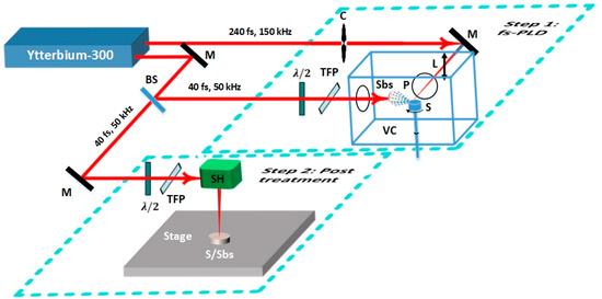
Figure 1.
Schematic diagram of the experimental setup: Step 1—femtosecond pulsed laser deposition of the source material, Step 2—post treatment of the sample in step 1 using scan head, Ytterbium-300—300 W ytterbium laser with 240 fs, 150 kHz and 40 fs, 50 kHz laser beams, C—Optical chopper, M—dielectric mirror, L—objective lens, VC—vacuum chamber, S—source material wrapped around a rotating cylindrical holder, P—plasma plume, Sbs—substrate, BS—beam splitter, —half wave plate, TFP—thin film polarizer, SH—scan head, S/Sbs—source material deposited over the substrate via fs-PLD, Stage—z-axis translation stage.
In the next step, the as-deposited Mo/MS sample was treated in air with 1.5 W, followed by 0.2 W laser power. The pulse duration was 40 fs and repetition rate was 50 kHz. For of 50 μm, the corresponding fluence values were 1.5 and 0.2 J/cm2, respectively. A scan head was employed to completely scan the sample surface. A parallel line scan of scan speed () 3325 mm/s and line spacing () (or 0.01 mm) was performed. The sample obtained after 1.5 J/cm2 treatment is named Mo-1.5/MS, whereas the sample obtained after 0.2 J/cm2 treatment of Mo-1.5/MS is termed as MoOx/MS.
For the purpose of structural comparison, polished MS without any coating was also laser-scanned with 1.5 J/cm2 followed by scanning with 0.2 J/cm2. The same pulse duration of 40 fs and repetition rate of 50 kHz were maintained.
The morphological and elemental studies were carried out with a TESCAN VEGA 3 LMU scanning electron microscope and an INCAx-act EDS detector from Oxford Instruments (Abingdon, UK). The 2D fast Fourier transforms (FFTs) were calculated from SEM micrographs with VegaTC 4.1.20.3 SEM software. The information about the chemical nature of the sample’s surface was acquired with a Renishaw inVia confocal Raman microscope (Wotton-under-Edge, UK) fitted with a 100× focusing lens. The excitation wavelength was 514 nm, and the power was 1.5 mW. For detailed crystallographic information and phase confirmation, X-ray diffraction analysis was conducted with an X’Pert3 Powder diffractometer from Panalytical (Malvern, UK) within a in the range. Topography and roughness measurements were acquired with hpAFM atomic force microscope from NANOMAGNETICS Instruments (Ankara, Turkey). The electrochemical measurements were performed with a CHI 660E electrochemical workstation of CH Instruments, Inc. (Austin, TX, USA). The open circuit potential () was let to stabilize in each case. Although the stability time was variable for each type of sample, before taking any measurements, it was ensured that there was a negligible change in with time. The scan rate was set to 0.001 V/s in the auto-sense mode. The voltage window was shifted relative to the for each sample.
3. Results and Discussion
Figure S1 presents camera images of the Mo/MS produced by the raw fs-PLD process (Figure S1a), the Mo-1.5/MS obtained after laser scanning of Mo/MS at 1.5 J/cm2 (Figure S1a), and MoOx/MS produced after laser-scanning the Mo-1.5/MS (Figure S1c) with 0.2 J/cm2. From the physical appearance, the Mo/MS is the darkest, hinting at the presence of rough light-scattering features on the surface responsible for reduced specular reflections [43]. Similarly, the Mo coat depicts a very low packing density and reduced adhesion with the MS substrate. The film can easily be washed off. With substrate heating, film adhesion improves marginally, but the structural non-uniformity still exists.
To improve the adhesion and uniformity of the Mo/MS coating, the constituent submicron particles in the Mo layer need to be fused together. Melting and resolidification of the Mo layer can mitigate the particles as well as improve adhesion. However, heating Mo to its melting point (i.e., 2623 °C) without damaging the substrate MS (with melting point = 1350–1530 °C) is impossible with conventional resistive heating techniques. In addition to Fe melting and diffusion into Mo, coating delamination and cracks formation at high temperatures is another concern. Therefore, selective heating of the top Mo layer to melt and oxidize Mo without damaging the substrate is inevitable. Femtosecond laser can impart very high peak power pulses (up to 7 GW) for very short durations and can instantly heat up Mo. Anticipating improvement in the quality of the top Mo layer, we proceeded to laser-scan Mo/MS.
After laser scanning Mo/MS at 1.5 J/cm2, the top Mo coat transformed into a slightly reflecting film. This demonstrates that the film has become much smoother and uniform compared to the as-deposited Mo/MS. Subsequent laser scanning at 0.2 J/cm2 transformed the topcoat into an almost transparent coating with the substrate visible through it. This change in color and transparency suggests that laser-induced physical and chemical changes have taken place on the sample surface.
SEM analysis was carried out to explore the associated morphological transformations. Figure 2 reveals that Mo/MS is actually composed of submicron particles ejected from the Mo source as ablation products. Since fs pulses have very high peak powers, such submicron ablation debris are expected [44], thus rendering very high deposition rates
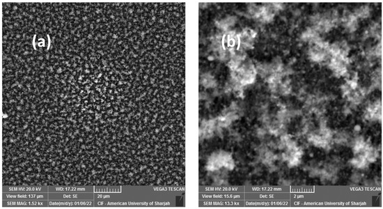
Figure 2.
SEM micrographs of the as-deposited Mo thin film over mild steel (Mo/MS) at view fields of (a) 137 and (b) 15.6 .
The surface morphology of the Mo-1.5/MS is quite different from that of Mo/MS. After the laser scan, the ablation debris are removed altogether, instead laser-induced periodic surface structures (LIPSS) with a period of around occupy the surface (Figure 3). Similarly, there are no deep ablation craters suggesting minimal ablation to have taken place.
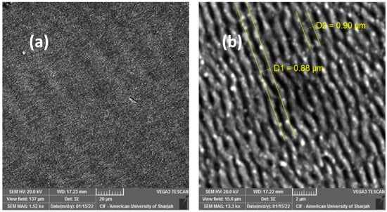
Figure 3.
SEM micrographs at (a) 1.5 kx and (b) 13.3 kx magnifications of Mo-1.5/MS obtained after laser-scanning the as-deposited Mo/MS with 40 fs pulses of 1.5 J/cm2 fluence and 50 kHz repetition rate.
Substoichiometric MoOx oxidizes at temperatures as low as 300 °C [45]. Similarly, Cuando-Espitia et al. [46] demonstrated that Mo thin films oxidize with fs laser treatment in air and at different oxygen partial pressures. To oxidize Mo-1.5/MS, the sample was laser-scanned eight times in ambient air with 0.2 J/cm2 pulses. As shown in Figure 4, the coating is uniform throughout, crack-free, and pore-free. Moreover, more uniform and finer LIPSS of periods covering the whole surface are observable. The scan with 1.5 J/cm2 was meant to melt the ablation debris so that they take the form of a uniform coat that strongly adheres to the MS substrate. The LIPSS that appeared due to the 1.5 J/cm2 treatment might have influenced the orientation and/or morphology of the subsequently appearing LIPSS due to the 0.2 J/cm2 treatment [47,48].
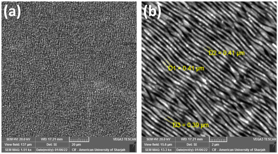
Figure 4.
SEM micrographs at (a) 1.5 kx and (b) 13.3 kx magnifications of MoOx/MS obtained after laser-scanning Mo-1.5/MS with 40 fs pulses of 0.2 J/cm2 fluence and 50 kHz repetition rate.
To analyze the periodicity and estimate the spatial period, 2D fast Fourier transforms (FFTs) of the SEM micrographs (Figure S4) of Mo-1.5/MS and MoOx/MS were acquired. Figure 5 details the corresponding FFTs. The period of the LIPSS observed on the Mo-1.5/MS is 0.86 . Since its more than half of the central laser wavelength, i.e., 1030 nm, we can categorize these as low spatial frequency LIPSS (LSFL) [49]. There are no other prominent periodic or quasi-periodic structures present on Mo-1.5/MS surface. On the other hand, the MoOx/MS depicts three different spatial periods correlatable with three distinct surface features. The most noticeable are the 0.41 LIPSS. Since the spatial period is less than half of the laser wavelength, we can categorize these as high spatial frequency LIPSS (HSFL) [49]. The other type of periodic surface features has an average spatial period close to 0.73 . These features are the remains of the LSFL which appeared on Mo/MS after 1.5 J/cm2 treatment. Their presence is somewhat overshadowed by the presence of HSFL in the corresponding SEM micrograph (Figure 4b) because multiple scans with 0.2 J/cm2 washed off the underlying LSFL almost completely. Similarly, the coinciding alignment directions of LSFL and HSFL as suggested in the FFT makes LSFL even less obvious in the SEM micrograph. The last among these features depicts a spatial period of around 1.7 . These features are identified in the SEM micrographs as the bigger wavy features aligned perpendicular to both LSFL and HSFL (Figure 4b) and Figure S4b). Since well-developed quasi-periodic grooves have a spatial period of 2–4 times that of the laser wavelength [50], and usually require multiple number of pulses (multiple scans in this case) [51,52], we believe that these features are grooves rudiments. It is known that reducing pulse fluence [53,54] and/or increasing the number of pulses [55] can result in the emergence of HSFL, therefore, HSFL found on MoOx/MS may either be due to the reduced pulse fluence (0.2 J/cm2) or increased number of scans (9 scans with line spacing), or both.
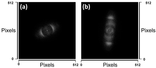
Figure 5.
2D Fourier transform of (a) Mo-1.5/MS and (b) MoOx/MS micrographs shown in Figure S4. The view field in either case is 48.1 .
The topography analysis of the coatings depicts average roughness (Ra) and root mean square roughness (Rq) of around 0.27 and 0.33 , respectively (Figure S5). Similarly, the thickness of the as-deposited Mo/MS was measured to be around (Figure S6a,b), which compressed to (Figure 6a,b) upon fs laser treatment. The reduction in thickness is indicative of the more compactness of the film. This is because the sequential 1.5 J/cm2 and 0.2 J/cm2 post-deposition scans fused the ablation debris of the as-deposited Mo/MS sample.
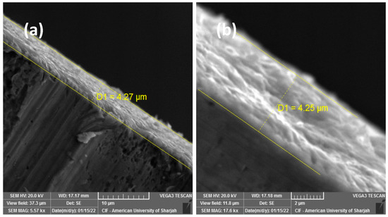
Figure 6.
Cross section of the MoOx deposited over mild steel observed at (a) 5.57 k× and (b) 17.6 k× magnifications.
The cross section of MoOx/MS was prepared after grinding it with abrasive papers without using any lubricant. The signature of the harsh grinding process is visible on the steel substrate, but we could not identify any huge chunks of MoOx removed during the grinding process, hinting at the amorphous nature of MoOx layer. Despite such a rigid grinding process, the film was found fully intact with the substrate and did not delaminate at all, suggesting its good adhesion with the substrate. We observed the cross section at different locations, but the film was found well intact with the substrate, with no observed delamination. The improved adhesion is most probably due to the Mo–Fe alloy system formation at the interface. The heated Mo in contact with the underlying Fe can easily fuse Fe. As a result, the energetic Fe from the substrate can also marginally diffuse into the top MoOx. The strong adhesion of the coat with the substrate suggests that the fs-laser induced instantaneous melting and solidification actually resulted in a strong Mo–Fe bond coat to hold the top MoOx well-adhered to the underlying MS. Though the laser pulse can excite the underlying MS through conduction or convection, it is not probable that the laser penetrates down to directly energize the MS substrate.
The effective penetration depth depends on the material as well as the laser pulse parameters. The ablation threshold of the precursor Mo is around 0.11–0.15 J/cm2 [26,56,57,58]. The average penetration depth of Mo was estimated to be around 16.5 nm for 6 fs pulses of fluence 0.15 J/cm2 [26]. Similarly, a penetration depth of 6 nm was reported for 500 fs pulses of fluence 0.3 J/cm2. The same study reported a penetration depth of around 18 nm for 1.5 J/cm2 fluence [56]. Interestingly, low-level ablation off the Mo surface persists even if the fluence was reduced to ¼ the ablation threshold (0.11 J/cm2) of Mo [29]. For the photoformed MoOx, the average threshold is around 0.6 J/cm2 for 8 ps pulses of 1064 nm [59], which is expected to decrease as the pulse duration decreases. This is because longer pulses have lower peak powers [60] and are associated with higher thermal diffusion, and deeper thermal propagation into the sample, therefore requiring relatively more energy than shorter pulses for ablation [59,60,61]. Nonetheless, the ablation threshold is expected to change with each scan due to the laser-induced compositional, morphological, structural, and optical changes associated with each scan [47]. Hence, in our study, it can be inferred that ablation takes place for both the 0.2 J/cm2 and 1.5 J/cm2 scans; however, for each pulse the ablation rate is of the order of a few nanometers [56]. For 50 μm spot size and 50 kHz repetition rate, a scan speed of 3325 mm/s gave a spot overlap rate of -33%, which is analogous to 16 μm separation between adjacent spots. The 16 μm separation ensured that each pulse hit the same spot only once per line scan. These measures ensured that the laser could not penetrate deep to hit the substrate. The film thickness and morphology are other indicators of the fact that the ablation rate was negligible for the laser to penetrate through the topcoat and hit the substrate. The loosely packed as-deposited 12 thick film was reduced to thick compact film after complete treatment. The uniform coverage of the sample with LIPSS and the absence of ablation craters are further evidence that the applied laser parameters (i.e., pulse duration (40 fs), the pule fluence (0.2–1.5 J/cm2), and the scan speed of 3325 mm/s) were optimum for inducing melting without causing excessive ablation.
Figure S2 depicts a mild steel surface structured with the same laser pulse and scan parameters as employed for MoOx/MS [56]. If the laser could penetrate into depths of the order of (which is MoOx thickness) or beyond, features similar to that of Figure S2 would have been observed. The structures for mild steel are due to higher ablation rate experienced at the same laser and scan settings.
We used confocal Raman microscopy to analyze the chemical nature of the sample’s surface. As shown in Figure 7, oxides of Mo were detected along the surface of the precursor Mo sheet, the as-deposited Mo/MS, and the fully treated MoOx/MS. We could trace different modes of vibrations in the 200–1000 cm−1 range related to different Mo oxide structures. Although Mo oxide exists in many polymorphic forms, the most stable orthorhombic structure of edge-sharing MoO6 octahedra was identified from the bands around 996 cm−1, 820 cm−1, 663 cm−1, 339 cm−1, and 285 cm−1 [62,63,64].
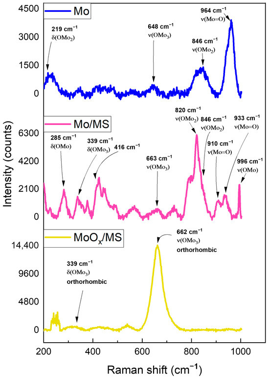
Figure 7.
Raman spectra of the molybdenum source (Mo), as-deposited molybdenum (Mo/MS), and fully treated molybdenum to obtain molybdenum oxide (MoOx/MS).
Mo generally prefers to stay in a body-centered cubic (BCC) structure, and it typically crystallizes into a BCC structure upon solidification. In some cases, it deposits as face-centered cubic (FCC) as well [65]. FCC and BCC metals have only acoustic phonons and no optical phonons, which are not detectable with Raman spectroscopy. Therefore, we do not see first-order Mo signals in any Raman spectra [66].
For the fully treated MoOx/MS, the preferred vibration mode determined is the three coordinated-edge OMo3 stretching and bending vibrations at 662 cm−1 and 339 cm−1, respectively. These bands signify the presence of a stable orthorhombic structure along the surface [64].
Although MoOx/MS was prepared in the air, there was no signature of any significant nitrides content on the surface. This is predominantly due to the reduced laser fluence (i.e., 1.5 J/cm2 and 0.2 J/cm2) used in the post-treatment process. Since each nitrogen molecule is composed of N atoms bonded by a very strong triple bond that requires 945 kJ mol−1 to break it [67], relatively small excitations are inefficient at producing significant quantities of nitrides. In comparison, each oxygen molecule is constituted of oxygen atoms bonded by a double bond between them, and breaking it requires an energy of 498 kJ mol−1. Likewise, the ionization potential of nitrogen into N3− equals 47.44 eV and is much higher than that of O to ionize it into O2− that is 35.11 eV. For these reasons, the free energy of formation is less negative for nitrides than that of similar oxides [68]. This is why we can only identify oxides but no nitrides in MoOx/MS.
The XRD patterns shown in Figure S7 suggest that there is no long-range order is MoOx/MS, though orthorhombic Mo oxide was confirmed from Raman analysis. Similarly, there is no crystalline Mo left in the sample either. The 1.5 J/cm2 treated sample is also fully amorphous. The Mo peak could only be observed in Mo/MS at 40.6, which indicates the preferred (110) texture of cubic Mo [69]. The amorphicity of the post-treated samples is attributed to the short excitation time associated with ultrashort pulses. The localized sudden heating and cooling do not render sufficient time for gradual relaxation. Similarly, O, which attaches to Mo during the laser-scanning process, does not find sufficient time to produce MoOx of large crystallite size.
The resultant film properties are a function of the fluence employed. Likewise, both physical and chemical properties of the film are subject to change with each scan. The number of successive scans play an essential role in shaping these properties. Since the sample was scanned at two different fluence values, i.e., at 1.5 J/cm2, followed by 8 times scanning at 0.2 J/cm2, different intrinsic film properties are anticipated for the two fluence regimes.
Among the fluence-dependent properties are chemical, structural, optical, and morphological characteristics of the topcoat. Due to the higher accumulated fluence, the fully treated i.e., 1.5 J/cm2 followed by 0.2 J/cm2 scanned sample (MoOx/MS) is more oxidized than the1.5 J/cm2 scanned sample (Mo-1.5/MS). This is due to the laser-induced oxygen plasma reacting with the topcoat and oxidizing it. Oxygen diffusion due to thermal and concentration gradients as well as melt hydrodynamic movement are associated phenomena for enhanced oxidation at higher accumulated fluence [70]. The O content in the interior of the MoOx layer may not be the same as that at the exterior surface. Actually, the O content may decrease as we traverse down towards the substrate. The microstructure and crystallinity are also affected by the instantaneous melting and solidification due to ultrafast laser-matter interaction. Usually amorphous/nanocrystalline films are obtained after short laser–matter interaction. The crystallinity has been evidenced to improve with increasing accumulated fluence [70]. This is because higher accumulated fluence induces more reactive oxygen species [71], which not only enhance the MoOx content but also improve the crystallinity of the topcoat [72,73]. Similarly, the high transparency of MoOx/MS relative to Mo-1.5/MS is due to the enhanced MoOx content that improved the overall transparency of MoOx/MS [74]. Among the morphological transformations, the most appealing morphological change was the appearance of HSFL and quasi-periodic grooves along with LSFL on the fully treated MoOx/MS. Changes in the ablation threshold of the topcoat due to compositional, morphological, structural, and optical changes associated with each scan are also inevitable [47].
As mentioned previously, although Mo and its compounds are used for many technological applications, we are more interested in determining the quality of the coating. As an application example, MoOx/MS was tested for corrosion inhibition in a simulated 3.5 wt% aqueous NaCl environment. The performance was evaluated in terms of corrosion inhibition efficiency (), which was, in turn calculated using the relation given below.
Here, and represent the corrosion current densities measured for the polished and MoOx coated mild steel, respectively. The average improvement recorded relative to polished MS was 94.83% (Figure 8 and Table 1). The average value was calculated by testing and averaging 5 MoOx/MS samples. The precursor pristine Mo had an average of % in an aqueous NaCl environment. Since MoOx/MS is substoichiometric and the oxygen content is less saturated, any oxygen vacancy will leave behind a Mo-dangling bond [75]. These dangling bonds and the higher surface area due to the laser-induced surface structures are believed to be the reasons for the lower relative to pristine Mo. The of MoOx/MS samples could be further improved by decreasing the surface area and fully oxygenating the sample.
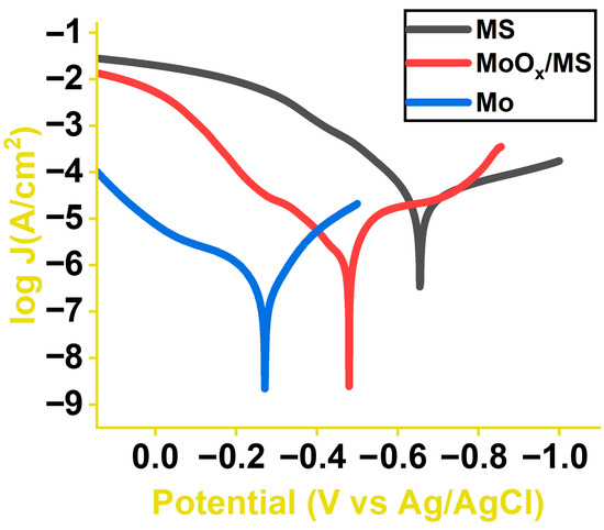
Figure 8.
Tafel plots of mild steel, molybdenum oxide deposited over mild steel, and molybdenum foil obtained in 3.5 wt% aqueous NaCl solution.

Table 1.
Polarization resistance and corrosion current calculated from Tafel extrapolation and compared.
4. Conclusions
A thin film deposition technology solely based on fs laser was introduced for depositing amorphous coatings of relatively high melting point materials (in this case, Mo). Despite the very high deposition rates achievable with this technique, the films are uniform, crack-free, pore-free, and well-adhering to the substrate. The method can be employed to achieve superb adhesion without substrate heating or roughening and with no bond coats required. The method comprises a very raw coating of the source material being deposited in a vacuum chamber employing a high-rate femtosecond pulsed laser deposition (fs-PLD), followed by thoroughly scanning the raw sample to transform it into a high-quality coating. As a manifestation of the technique, a raw Mo film of around 12 thickness was deposited from a rotating molybdenum source in a vacuum chamber at 0.5 J/cm2. To obtain a good quality substoichiometric molybdenum oxide layer from the raw deposited Mo, it was further scanned thoroughly, first with 1.5 J/cm2 and then with 0.2 J/cm2 pulse fluence, while maintaining a scan rate and line spacing of 3325 mm/s and 10 , respectively. The substoichiometric molybdenum oxide’s corrosion inhibition efficiency () was analyzed in a 3.5 wt% aqueous NaCl environment. Compared to polished mild steel, an average corrosion inhibition efficiency of 94.83% was achieved.
Supplementary Materials
The following supporting information can be downloaded at: https://www.mdpi.com/1996-1944/16/3/909/s1.
Author Contributions
Conceptualization, A.S.A.; Methodology, A.A., P.P., T.N. and S.A.; Formal analysis, A.A.; Investigation, A.A., P.P., T.I. and M.K.; Resources, A.S.A.; Writing—review & editing, A.A., P.P. and A.S.A.; Supervision, A.S.A.; Project administration, A.S.A. All authors have read and agreed to the published version of the manuscript.
Funding
This research was funded by the American University of Sharjah, United Arab Emirates under FRG grant # FRG19-L-S61.
Informed Consent Statement
Not applicable.
Data Availability Statement
Data underlying the results presented in this paper are not publicly available at this time but may be obtained from the authors upon reasonable request.
Acknowledgments
We thank Hussain Alawadhi from the University of Sharjah for help with the Raman measurements.
Conflicts of Interest
The authors declare no conflict of interest.
Correction Statement
This article has been republished with a minor correction to the reference [35]. This change does not affect the scientific content of the article.
References
- Bai, S.; Liu, J.; Yang, P.; Huang, H.; Yang, L.-M. Femtosecond fiber laser additive manufacturing of tungsten. Laser 3d Manuf. III 2016, 9738, 96–105. [Google Scholar] [CrossRef]
- Sugioka, K.; Cheng, Y. Ultrafast lasers—Reliable tools for advanced materials processing. Light. Sci. Appl. 2014, 3, e149. [Google Scholar] [CrossRef]
- Vaida, M.E.; Gleitsmann, T.; Tchitnga, R.; Bernhardt, T.M. Femtosecond-Laser Photoemission Spectroscopy of Mo(100) Covered by Ultrathin MgO(100) Films of Variable Thickness. J. Phys. Chem. C 2009, 113, 10264–10268. [Google Scholar] [CrossRef]
- Cerullo, G.; De Silvestri, S. Ultrafast optical parametric amplifiers. Rev. Sci. Instrum. 2003, 74, 1–18. [Google Scholar] [CrossRef]
- Fuchs, S.; Wünsche, M.; Nathanael, J.; Abel, J.J.; Rödel, C.; Biedermann, J.; Reinhard, J.; Hübner, U.; Paulus, G.G. Optical coherence tomography with nanoscale axial resolution using a laser-driven high-harmonic source. Optica 2017, 4, 903–906. [Google Scholar] [CrossRef]
- Shah, J. Ultrafast Spectroscopy of Semiconductors and Semiconductor Nanostructures; Springer: Berlin, Germany, 1999; p. 115. [Google Scholar] [CrossRef]
- Buldt, J.; Mueller, M.; Stark, H.; Jauregui, C.; Limpert, J. Fiber laser-driven gas plasma-based generation of THz radiation with 50-mW average power. Appl. Phys. B Laser Opt. 2019, 126, 1–5. [Google Scholar] [CrossRef]
- Roberts, H.W.; Day, A.; O’Brart, D.P.S. Femtosecond laser–assisted cataract surgery: A review. Eur. J. Ophthalmol. 2019, 30, 417–429. [Google Scholar] [CrossRef]
- Ahmad, S.; Egilmez, M.; Iqbal, M.; Ibrahim, T.; Khamis, M.; Alnaser, A.S. Pulsed Laser Deposited Zeolite Coatings on Femtosecond Laser-Nanostructured Steel Meshes for Durable Superhydrophilic/Oleophobic Functionalities. Front. Chem. 2021, 9, 1027. [Google Scholar] [CrossRef]
- Stuke, M. Femtosecond uv excimer laser ablation. Appl. Phys. B Laser Opt. 1987, 44, 199–204. [Google Scholar] [CrossRef]
- Srinivasan, R.; Sutcliffe, E.; Braren, B. Ablation and etching of polymethylmethacrylate by very short (160 fs) ultraviolet (308 nm) laser pulses. Appl. Phys. Lett. 1987, 51, 1285–1287. [Google Scholar] [CrossRef]
- Davis, K.M.; Miura, K.; Sugimoto, N.; Hirao, K. Writing waveguides in glass with a femtosecond laser. Opt. Lett. 1996, 21, 1729–1731. [Google Scholar] [CrossRef] [PubMed]
- Son, Y.; Yeo, J.; Moon, H.; Lim, T.W.; Hong, S.; Nam, K.H.; Yoo, S.; Grigoropoulos, C.P.; Yang, D.-Y.; Ko, S.H. Nanoscale Electronics: Digital Fabrication by Direct Femtosecond Laser Processing of Metal Nanoparticles. Adv. Mater. 2011, 23, 3176–3181. [Google Scholar] [CrossRef] [PubMed]
- Carey, J.E., III. Femtosecond-Laser Microstructuring of Silicon for Novel Optoelectronic Devices. Ph.D. Thesis, Harvard University, Cambridge, MA, USA, 2004. Available online: https://ui.adsabs.harvard.edu/abs/2004PhDT.......164C/abstract (accessed on 20 December 2022).
- Della Valle, G.; Osellame, R.; LaPorta, P. Micromachining of photonic devices by femtosecond laser pulses. J. Opt. A Pure Appl. Opt. 2008, 11, 013001. [Google Scholar] [CrossRef]
- Halbwax, M.; Sarnet, T.; Delaporte, P.; Sentis, M.; Etienne, H.; Torregrosa, F.; Vervisch, V.; Perichaud, I.; Martinuzzi, S. Micro and nano-structuration of silicon by femtosecond laser: Application to silicon photovoltaic cells fabrication. Thin Solid Films 2008, 516, 6791–6795. [Google Scholar] [CrossRef]
- Chai, N.; Liu, Y.; Yue, Y.; Wei, P.; Wang, X.; Zhao, J.; Zhang, Q.; Huang, F.; Zeng, Z.; Gan, Z.; et al. 3D nonlinear photolithography of Tin oxide ceramics via femtosecond laser. Sci. China Mater. 2021, 64, 1477–1484. [Google Scholar] [CrossRef]
- Cheng, Y.; Sugioka, K.; Midorikawa, K.; Masuda, M.; Toyoda, K.; Kawachi, M.; Shihoyama, K. Control of the cross-sectional shape of a hollow microchannel embedded in photostructurable glass by use of a femtosecond laser. Opt. Lett. 2003, 28, 55–57. [Google Scholar] [CrossRef]
- Sugioka, K.; Cheng, Y. Femtosecond laser processing for optofluidic fabrication. Lab A Chip 2012, 12, 3576–3589. [Google Scholar] [CrossRef] [PubMed]
- Wang, K.; Zhang, B.; Xie, W.; Liu, S.; Wei, X.; Cai, Z.; Gu, M.; Tao, Y.; Yang, T.; Zhang, C.; et al. Coupling Among Carriers and Phonons in Femtosecond Laser Pulses Excited SrRuO3: A Promising Candidate for Optomechanical and Optoelectronic Applications. ACS Appl. Nano Mater. 2019, 2, 3882–3888. [Google Scholar] [CrossRef]
- Kaligar, A.B.; Kumar, H.A.; Ali, A.; Abuzaid, W.; Egilmez, M.; Alkhader, M.; Abed, F.; Alnaser, A.S. Femtosecond Laser-Based Additive Manufacturing: Current Status and Perspectives. Quantum Beam Sci. 2022, 6, 5. [Google Scholar] [CrossRef]
- Lu, J.; Huang, T.; Liu, Z.; Zhang, X.; Xiao, R. Long-term wettability of titanium surfaces by combined femtosecond laser micro/nano structuring and chemical treatments. Appl. Surf. Sci. 2018, 459, 257–262. [Google Scholar] [CrossRef]
- Tamaki, T.; Watanabe, W.; Nishii, J.; Itoh, K. Welding of Transparent Materials Using Femtosecond Laser Pulses. Jpn. J. Appl. Phys. 2005, 44, L687. [Google Scholar] [CrossRef]
- Ahmad, S.; Ahmad, W.; Abu Baker, A.; Egilmez, M.; Abuzaid, W.; Orhan, M.F.; Ibrahim, T.; Khamis, M.; Alnaser, A.S. Enhancement of the corrosion resistance of mild steel with femtosecond laser- nanostructuring and CrCoNi medium entropy alloy coating. Appl. Surf. Sci. Adv. 2022, 12. [Google Scholar] [CrossRef]
- Lim, Y.C.; Johnson, J.; Fei, Z.; Wu, Y.; Farson, D.F.; Lannutti, J.J.; Choi, H.W.; Lee, L.J. Micropatterning and characterization of electrospun poly(ε-caprolactone)/gelatin nanofiber tissue scaffolds by femtosecond laser ablation for tissue engineering applications. Biotechnol. Bioeng. 2010, 108, 116–126. [Google Scholar] [CrossRef]
- Zhao, D.; Gierse, N.; Wegner, J.; Pretzler, G.; Oelmann, J.; Brezinsek, S.; Liang, Y.; Neubauer, O.; Rasinski, M.; Linsmeier, C.; et al. Ablation mass features in multi-pulses femtosecond laser ablate molybdenum target. Nucl. Instrum. Methods Phys. Res. Sect. B Beam Interact. Mater. Atoms 2018, 418, 54–59. [Google Scholar] [CrossRef]
- Kotsedi, L.; Mthunzi, P.; Nuru, Z.; Eaton, S.; Sechoghela, P.; Mongwaketsi, N.; Ramponi, R.; Maaza, M. Femtosecond laser surface structuring of molybdenum thin films. Appl. Surf. Sci. 2015, 353, 1334–1341. [Google Scholar] [CrossRef]
- Kotsedi, L.; Kaviyarasu, K.; Fuku, X.; Eaton, S.; Amara, E.; Bireche, F.; Ramponi, R.; Maaza, M. Two temperature approach to femtosecond laser oxidation of molybdenum and morphological study. Appl. Surf. Sci. 2017, 421, 213–219. [Google Scholar] [CrossRef]
- Cano-Lara, M.; Camacho-López, S.; Esparza-García, A.; Camacho-López, M. Laser-induced molybdenum oxide formation by low energy (nJ)–high repetition rate (MHz) femtosecond pulses. Opt. Mater. 2011, 33, 1648–1653. [Google Scholar] [CrossRef]
- Vorobyev, A.Y.; Guo, C. Direct femtosecond laser surface nano/microstructuring and its applications. Laser Photonics Rev. 2013, 7, 385–407. [Google Scholar] [CrossRef]
- Ganin, D.; Lapshin, K.; Obidin, A.; Vartapetov, S. Single-pulse perforation of thin transparent dielectrics by femtosecond lasers. Appl. Phys. A 2017, 123, 1–7. [Google Scholar] [CrossRef]
- Murray, M.; Jose, G.; Richards, B.; Jha, A. Femtosecond pulsed laser deposition of silicon thin films. Nanoscale Res. Lett. 2013, 8, 272. [Google Scholar] [CrossRef]
- Wasa, K.; Kitabatake, M.; Adachi, H. Thin Film Processes. In Thin Film Materials Technology; Elsevier: Amsterdam, The Netherlands, 2004; pp. 17–69. [Google Scholar] [CrossRef]
- Frey, H.; Khan, H.R. Handbook of Thin-Film Technology. In Handbook of Thin-Film Technology; Springer: Berlin, Germany, 2015; pp. 1–379. [Google Scholar] [CrossRef]
- Vencl, A. Optimisation of the deposition parameters of thick atmospheric plasma spray coatings. J. Balk. Tribol. Assoc. 2012, 18, 405–414. [Google Scholar]
- Chkalov, R.V.; Chkalova, D.G. Pulsed Laser Deposition of Thin-Film Coatings in an Electrostatic Field. Defect Diffus. Forum 2021, 410, 753–757. [Google Scholar] [CrossRef]
- Chkalov, R.V.; Chkalova, D.G. Collection of Laser Ablation Products by Means of an Electrostatic Field. Defect Diffus. Forum 2021, 410, 748–752. [Google Scholar] [CrossRef]
- Kumi-Barimah, E.; Penhale-Jones, R.; Salimian, A.; Upadhyaya, H.; Hasnath, A.; Jose, G. Phase evolution, morphological, optical and electrical properties of femtosecond pulsed laser deposited TiO2 thin films. Sci. Rep. 2020, 10, 1–12. [Google Scholar] [CrossRef] [PubMed]
- Okoshi, M.; Higashikawa, K.; Hanabusa, M. Pulsed laser deposition of ZnO thin films using a femtosecond laser. Appl. Surf. Sci. 2000, 154–155, 424–427. [Google Scholar] [CrossRef]
- Varacalle, D.J.; Guillen, D.; Deason, D.M.; Rhodaberger, W.; Sampson, E. Effect of Grit-Blasting on Substrate Roughness and Coating Adhesion. J. Therm. Spray Technol. 2006, 15, 348–355. [Google Scholar] [CrossRef]
- El-Shabasy, M. Perspective of adhesion of thin films. Period. Polytech. Electr. Eng. (Arch.) 1981, 25, 123–134. [Google Scholar]
- Lunk, H.-J.; Hartl, H. Discovery, properties and applications of molybdenum and its compounds. Chemtexts 2017, 3, 13. [Google Scholar] [CrossRef]
- Thirunaukkarasu, K.; Taher, A.; Chaudhary, N.; Rajput, V.K.; Naik, C.A.; Gautam, J.P.; Naraharisetty, S.R.G. Mechanically and thermally stable thin sheets of broadband antireflection surfaces fabricated by femtosecond lasers. Opt. Laser Technol. 2022, 150, 107935. [Google Scholar] [CrossRef]
- Sanz, M.; Walczak, M.; de Nalda, R.; Oujja, M.; Marco, J.F.; Rodriguez, J.; Izquierdo, J.G.; Bañares, L.; Castillejo, M. Femtosecond pulsed laser deposition of nanostructured TiO2 films. Appl. Surf. Sci. 2008, 255, 5206–5210. [Google Scholar] [CrossRef]
- Kihlborg, L. Studies on molybdenum oxides. Acta. Chem. Scand 1959, 13, 962. Available online: http://actachemscand.org/pdf/acta_vol_13_p0954-0962.pdf (accessed on 20 December 2022). [CrossRef]
- Cuando-Espitia, N.; Redenius, J.; Mensink, K.; Camacho-López, M.; Camacho-López, S.; Aguilar, G. Influence of oxygen pressure on the fs laser-induced oxidation of molybdenum thin films. Opt. Mater. Express 2018, 8, 581–596. [Google Scholar] [CrossRef]
- Girolami, M.; Bellucci, A.; Mastellone, M.; Orlando, S.; Valentini, V.; Montereali, R.; Vincenti, M.; Polini, R.; Trucchi, D.M. Optical characterization of double-nanotextured black diamond films. Carbon 2018, 138, 384–389. [Google Scholar] [CrossRef]
- Prada-Rodrigo, J.; Rodríguez-Beltrán, R.I.; Ezquerra, T.A.; Moreno, P.; Rebollar, E. Influence of film thickness and substrate roughness on the formation of laser induced periodic surface structures in poly(ethylene terephthalate) films deposited over gold substrates. Opt. Laser Technol. 2023, 159, 109007. [Google Scholar] [CrossRef]
- Bonse, J.; Gräf, S. Maxwell Meets Marangoni—A Review of Theories on Laser-Induced Periodic Surface Structures. Laser Photon- Rev. 2020, 14, 2000215. [Google Scholar] [CrossRef]
- He, S.; Nivas, J.J.; Anoop, K.; Vecchione, A.; Hu, M.; Bruzzese, R.; Amoruso, S. Surface structures induced by ultrashort laser pulses: Formation mechanisms of ripples and grooves. Appl. Surf. Sci. 2015, 353, 1214–1222. [Google Scholar] [CrossRef]
- He, S.; Nivas, J.J.; Vecchione, A.; Hu, M.; Amoruso, S. On the generation of grooves on crystalline silicon irradiated by femtosecond laser pulses. Opt. Express 2016, 24, 3238–3247. [Google Scholar] [CrossRef]
- Nivas, J.; Amoruso, S. Generation of Supra-Wavelength Grooves in Femtosecond Laser Surface Structuring of Silicon. Nanomaterials 2021, 11, 174. [Google Scholar] [CrossRef]
- Shi, X.; Xu, X. Laser fluence dependence of ripple formation on fused silica by femtosecond laser irradiation. Appl. Phys. A 2019, 125, 256. [Google Scholar] [CrossRef]
- Abere, M.J.; Zhong, M.; Krüger, J.; Bonse, J. Ultrafast laser-induced morphological transformations. MRS Bull. 2016, 41, 969–974. [Google Scholar] [CrossRef]
- Lin, X.; Li, X.; Zhang, Y.; Xie, C.; Liu, K.; Zhou, Q. Periodic structures on germanium induced by high repetition rate femtosecond laser. Opt. Laser Technol. 2017, 101, 291–297. [Google Scholar] [CrossRef]
- Preuss, S.; Demchuk, A.; Stuke, M. Sub-picosecond UV laser ablation of metals. Appl. Phys. A 1995, 61, 33–37. [Google Scholar] [CrossRef][Green Version]
- Shirk, M.D.; Molian, P.A. A review of ultrashort pulsed laser ablation of materials. J. Laser Appl. 1998, 10, 18–28. [Google Scholar] [CrossRef]
- Hermann, J.; Benfarah, M.; Coustillier, G.; Bruneau, S.; Axente, E.; Guillemoles, J.-F.; Sentis, M.; Alloncle, P.; Itina, T. Selective ablation of thin films with short and ultrashort laser pulses. Appl. Surf. Sci. 2006, 252, 4814–4818. [Google Scholar] [CrossRef]
- Munoz-Garcia, C.; Canteli, D.; Lauzurica, S.; Morales, M.; Molpeceres, C.; Ros, E.; Ortega, P.; López-González, J.; Voz, C. Influence of wavelength and pulse duration on the selective laser ablation of WOx, VOx and MoOx thin films. Surf. Interfaces 2021, 28, 101613. [Google Scholar] [CrossRef]
- Backus, S.; Durfee, C.G.; Murnane, M.M.; Kapteyn, H. High power ultrafast lasers. Rev. Sci. Instrum. 1998, 69, 1207–1223. [Google Scholar] [CrossRef]
- Chichkov, B.N.; Momma, C.; Nolte, S.; von Alvensleben, F.; Tünnermann, A. Femtosecond, picosecond and nanosecond laser ablation of solids. Appl. Phys. A Mater. Sci. Process 1996, 63, 109–115. [Google Scholar] [CrossRef]
- Aleksandrov, L.; Komatsu, T.; Iordanova, R.; Dimitriev, Y. Structure study of MoO3–ZnO–B2O3 glasses by Raman spectroscopy and formation of α-ZnMoO4 nanocrystals. Opt. Mater. 2011, 33, 839–845. [Google Scholar] [CrossRef]
- Velvarská, R.; Tišler, Z.; Raichlová, V.; Hidalgo-Herrador, J.M. Raman Spectroscopy as Molybdenum and Tungsten Content Analysis Tool for Mesoporous Silica and Beta Zeolite Catalysts. Molecules 2020, 25, 4918. [Google Scholar] [CrossRef]
- Chae, B.; Jung, Y.M.; Wu, X.; Bin Kim, S. Characterization of a series of sodium molybdate structures by two-dimensional Raman correlation analysis. J. Raman Spectrosc. 2003, 34, 451–458. [Google Scholar] [CrossRef]
- Das, R.; Deo, M.; Mukherjee, J.; Rao, M.R. Strain induced FCC to BCC structural change in sputtered molybdenum thin films. Surf. Coat. Technol. 2018, 353, 292–299. [Google Scholar] [CrossRef]
- Creighton, J.; Withnall, R. The Raman spectrum of gallium metal. Chem. Phys. Lett. 2000, 326, 311–313. [Google Scholar] [CrossRef]
- Geng, C.; Li, J.; Weiske, T.; Schwarz, H. Complete cleavage of the N≡N triple bond by Ta2N+ via degenerate ligand exchange at ambient temperature: A perfect catalytic cycle. Proc. Natl. Acad. Sci. USA 2019, 116, 21416–21420. [Google Scholar] [CrossRef] [PubMed]
- Lide, D.R. CRC Handbook of Chemistry and Physics: A Ready-Reference Book of Chemical and Phyical Data; CRC Press: Boca Raton, FL, USA, 1990. [Google Scholar]
- Dongil, A.B.; Conesa, J.M.; Pastor-Pérez, L.; Sepúlveda-Escribano, A.; Guerrero-Ruiz, A.; Rodríguez-Ramos, I. Carbothermally generated copper–molybdenum carbide supported on graphite for the CO2 hydrogenation to methanol. Catal. Sci. Technol. 2021, 11, 4051–4059. [Google Scholar] [CrossRef]
- Ali, A.; Piatkowski, P.A.; Alawadhi, H.; Alnaser, A.S. Reducing the Cut-In Voltage of a Silicon Carbide/p-Silicon Heterojunction Diode Using Femtosecond Laser Ablation. ACS Appl. Electron. Mater. 2022, 4, 6076–6086. [Google Scholar] [CrossRef]
- Zhang, S.; Wang, X.; He, M.; Jiang, Y.; Zhang, B.; Hang, W.; Huang, B. Laser-induced plasma temperature. Spectrochim. Acta Part B At. Spectrosc. 2014, 97, 13–33. [Google Scholar] [CrossRef]
- Sun, X.; Ehrhardt, M.; Lotnyk, A.; Lorenz, P.; Thelander, E.; Gerlach, J.W.; Smausz, T.; Decker, U.; Rauschenbach, B. Crystallization of Ge2Sb2Te5 thin films by nano- and femtosecond single laser pulse irradiation. Sci. Rep. 2016, 6, 28246. [Google Scholar] [CrossRef] [PubMed]
- Jang, J.; Oh, J.Y.; Kim, S.K.; Choi, Y.J.; Yoon, S.Y.; Kim, C.O. Electric-field-enhanced crystallization of amorphous silicon. Nature 1998, 395, 481–483. [Google Scholar] [CrossRef]
- Oh, M.S.; Yang, B.S.; Lee, J.H.; Oh, S.H.; Lee, U.S.; Kim, Y.J.; Kim, H.J.; Huh, M.S. Improvement of electrical and optical properties of molybdenum oxide thin films by ultralow pressure sputtering method. J. Vac. Sci. Technol. A 2012, 30, 031501. [Google Scholar] [CrossRef]
- Kc, S.; Longo, R.C.; Addou, R.; Wallace, R.M.; Cho, K. Electronic properties of MoS2/MoOx interfaces: Implications in Tunnel Field Effect Transistors and Hole Contacts. Sci. Rep. 2016, 6, 33562. [Google Scholar] [CrossRef]


Disclaimer/Publisher’s Note: The statements, opinions and data contained in all publications are solely those of the individual author(s) and contributor(s) and not of MDPI and/or the editor(s). MDPI and/or the editor(s) disclaim responsibility for any injury to people or property resulting from any ideas, methods, instructions or products referred to in the content. |
© 2023 by the authors. Licensee MDPI, Basel, Switzerland. This article is an open access article distributed under the terms and conditions of the Creative Commons Attribution (CC BY) license (https://creativecommons.org/licenses/by/4.0/).