
Improving the p-Type CuCrO2 Thin Film’s Electrical and Optical Properties
 ,
,  ,
,
Abstract
1. Introduction
2. Materials and Methods
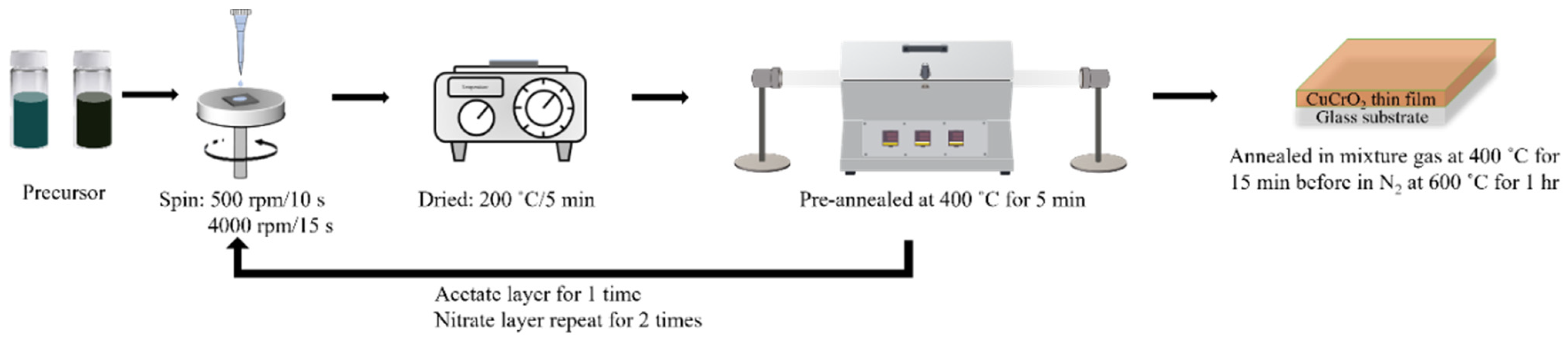
2.1. Preparation of CuCrO2 Solution
2.2. Preparation of CuCrO2 Thin Films by Spin Coating
2.3. Characterization of CuCrO2 Thin Films by Spin Coating
3. Results
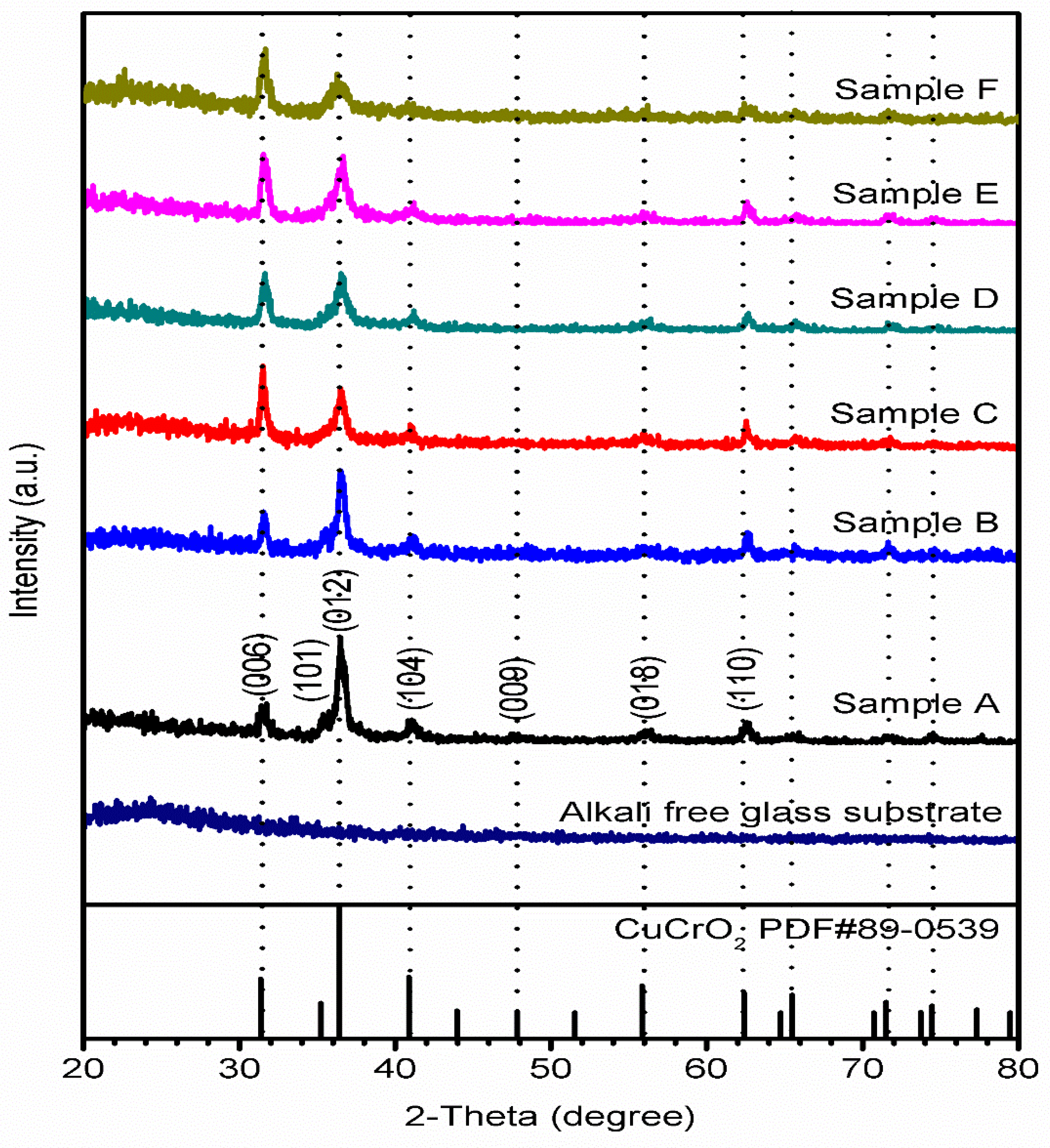
3.1. XRD Analysis
3.2. SEM Studies
3.3. UV-Vis Analysis
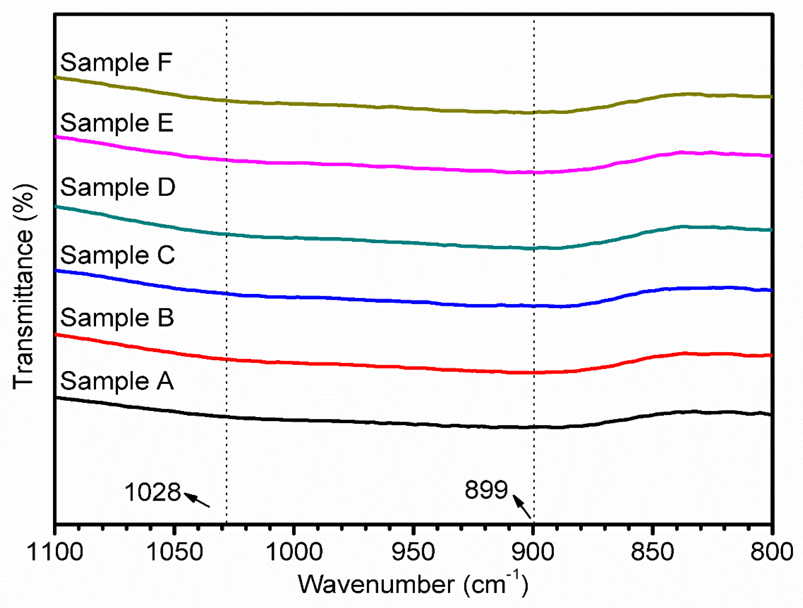
3.4. FT-IR Analysis
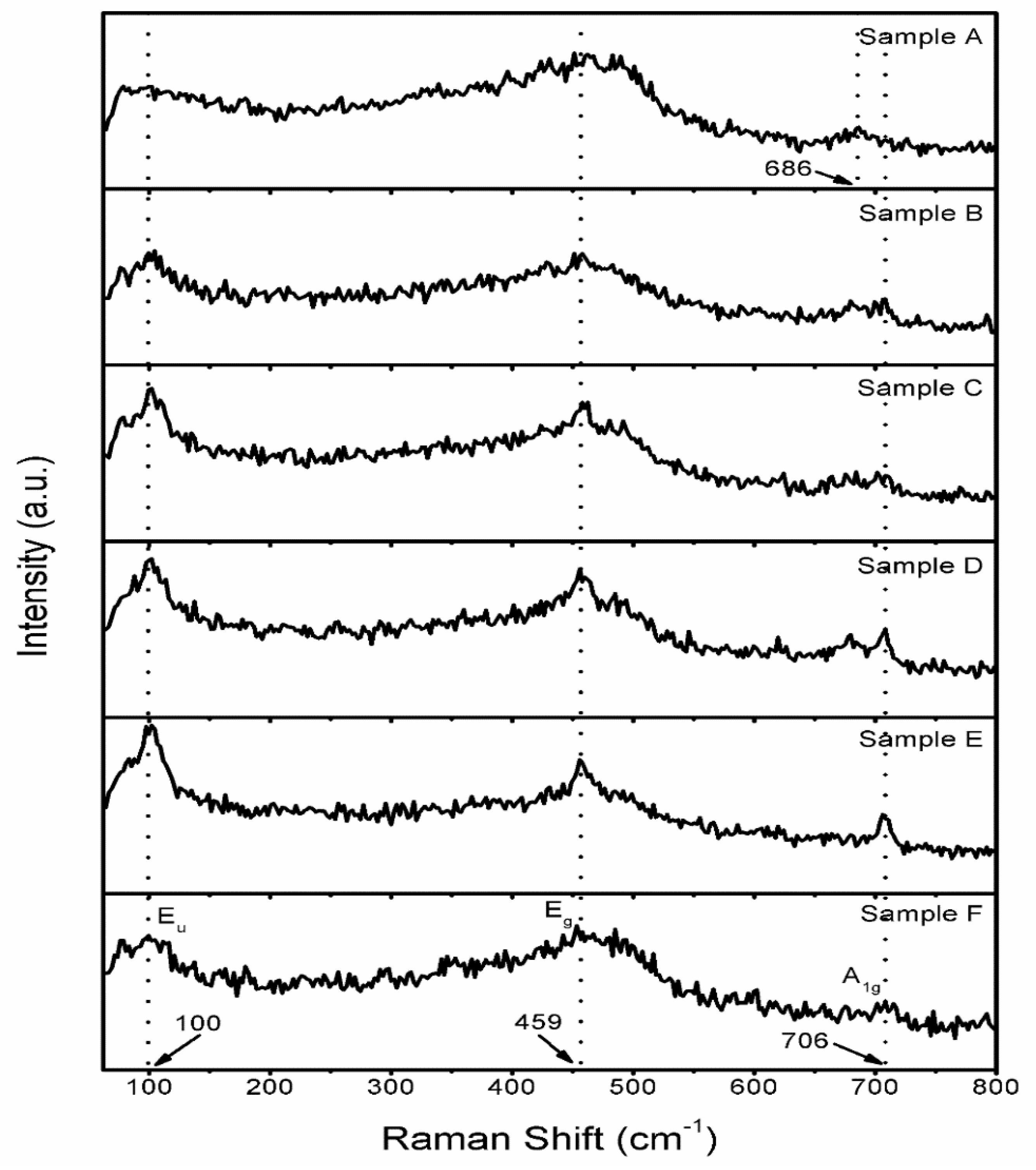
3.5. Raman Studies
4. Electrical Properties and Figure of Merit (FOM)
5. Conclusions
Author Contributions
Funding
Institutional Review Board Statement
Informed Consent Statement
Data Availability Statement
Conflicts of Interest
References
- Abdelwahab, H.M.; Ratep, A.; Elsoud, A.A.; Boshta, M.; Osman, M.B.S. Influences of annealing temperature on sprayed CuFeO2 thin films. Results Phys. 2018, 9, 1112–1115. [Google Scholar] [CrossRef]
- Sarkar, D.K.; Mahmud Hasan, A.K.; Mottakin, M.; Selvanathan, V.; Sobayel, K.; Islam, M.A.; Muhammad, G.; Aminuzzaman, M.; Shahiduzzaman, M.; Sopian, K.; et al. Lead free efficient perovskite solar cell device Optimization and defect study using Mg doped CuCrO2 as HTL and WO3 as ETL. Sol. Energy 2022, 243, 215–224. [Google Scholar] [CrossRef]
- Bottiglieri, L.; Resende, J.; Weber, M.; Chaix-Pluchery, O.; Jiménez, C.; Deschanvres, J. Out of stoichiometry CuCrO2 films as a promising p-type TCO for transparent electronics. Mater. Adv. 2021, 2, 4721–4732. [Google Scholar] [CrossRef]
- Sun, S.; Xu, M.; Zhang, Y.; Liu, R.; Wang, X.; Zhang, L.; Fang, Y.; Wang, P. Study of molybdenum oxide optimized hole carrier transport in perovskite solar cells. Org. Electron. 2022, 113, 106697. [Google Scholar] [CrossRef]
- Moreira, M.; Afonso, J.; Crepelliere, J.; Lenoble, D.; Lunca-Popa, P. A review on the p-type transparent Cu–Cr–O delafossite materials. J. Mater. Sci. 2022, 57, 3114–3142. [Google Scholar] [CrossRef]
- Zhamatuofu, B.; Chen, S.-C.; Lin, S.-S.; Shi, Q.; Lu, Y.-B.; Song, S.-M.; Sun, H. Review in optoelectronic properties of p-type CuCrO2 transparent conductive films. Surf. Interfaces 2021, 22, 100824. [Google Scholar]
- Renuka, H.; Garudapalli, A.; Raman, T.S.A.; Venkataraman, B.H.; Ramaswamy, K.; Raju, K.C.J.; Goel, S.; Kundu, S. Enhanced photovoltaic response in ferroelectric Ti-doped BFO heterojunction through interface engineering for building integrated applications. Sol. Energy 2021, 225, 863–874. [Google Scholar] [CrossRef]
- Dunlap-Shohl, W.A.; Daunis, T.B.; Wang, X.; Wang, J.; Zhang, B.; Barrera, D.; Yan, Y.; Hsu, J.W.P.; Mitzi, D.B. Room-temperature fabrication of a delafossite CuCrO2 hole transport layer for perovskite solar cells. J. Mater. Chem. A Mater 2018, 6, 469–477. [Google Scholar] [CrossRef]
- Dordor, P.; Chaminade, J.P.; Wichainchai, A.; Marquestaut, E.; Doumerc, J.P.; Pouchard, M.; Hagenmuller, P.; Ammar, A. Crystal growth and electrical properties of CuFeO2 single crystals. J. Solid State Chem. 1988, 75, 105–112. [Google Scholar] [CrossRef]
- Harada, T. Thin-film growth and application prospects of metallic delafossites. In Materials Today Advances; Elsevier Ltd.: Amsterdam, The Netherlands, 2021; Volume 11. [Google Scholar] [CrossRef]
- Poienar, M.; Hardy, V.; Kundys, B.; Singh, K.; Maignan, A.; Damay, F.; Martin, C. Revisiting the properties of delafossite CuCrO2: A single crystal study. J. Solid State Chem. 2012, 185, 56–61. [Google Scholar] [CrossRef]
- Narro-Ríos, J.S.; Garduño-Wilches, I.; Alarcón-Flores, G.; Ruiz-Rojas, C.; Gómez-Lizárraga, K.; Aguilar-Frutis, M. Spray pyrolysis synthesis of a semi-transparent p-CuCrO2/n-ZnO heterojunction: Structural, optical, and electrical properties. Phys. B Condens. Matter 2022, 624, 413426. [Google Scholar] [CrossRef]
- Van Hoang, D.; Pham, A.; Baba, T.; Nguyen, T.; Le, T.; Ung, T.; Hong, J.; Bae, J.; Park, H.; Park, S.; et al. New record high thermoelectric ZT of delafossite-based CuCrO2 thin films obtained by simultaneously reducing electrical resistivity and thermal conductivity via heavy doping with controlled residual stress. Appl. Surf. Sci. 2022, 583, 152526. [Google Scholar] [CrossRef]
- Lin, S.H.; Yeh, R.; Chu, C.; Yu, R.S. Effects of Mg doping on structural and optoelectronic properties of p-type semiconductor CuCrO2 thin films. Mater Sci. Semicond. Process. 2022, 139, 106346. [Google Scholar] [CrossRef]
- Milisavljevic, I.; Wu, Y. Tb-doped β-(AlxGa1-x)2O3 epitaxial films on c-sapphire substrates fabricated via a spin-coating method. J. Alloys Compd. 2022, 928, 167208. [Google Scholar] [CrossRef]
- Yu, C.L.; Sakthinathan, S.; Lu, M.-T.; Yu, S.-T.; Kuo, C.-Y.; You, Y.-F.; Chiu, T.-W. CuAlO2/AlN double-layer thin film prepared by the spin coating approach. Thin Solid Film. 2022, 753, 139260. [Google Scholar] [CrossRef]
- Benrezgua, E.; Sakthinathan, S.; Lu, M.-T.; Yu, S.-T.; Kuo, C.-Y.; You, Y.-F.; Chiu, T.-W. Synthesis and properties of copper doped zinc oxide thin films by sol-gel, spin coating and dipping: A characterization review. J. Mol. Struct. 2022, 1267, 139260. [Google Scholar] [CrossRef]
- Cho, A.; Banu, S.; Cho, Y.; Ahn, S.; Yun, J.; Cho, J.S. The effect of metal-chelate complex in Cu2SnS3 thin film solar cells and their characteristics, photovoltaic performance, and defect analysis. Sol. Energy 2019, 185, 131–145. [Google Scholar] [CrossRef]
- Yu, M.; Liang, M.; Liu, J.; Li, S.; Xue, B.; Zhao, H. Effect of chelating agent acetylacetone on corrosion protection properties of silane-zirconium sol-gel coatings. Appl. Surf. Sci. 2016, 363, 229–239. [Google Scholar] [CrossRef]
- Marin, O.; Tirado, M.; Budini, N.; Mosquera, E.; Figueroa, C.; Comedi, D. Photoluminescence from c-axis oriented ZnO films synthesized by sol-gel with diethanolamine as chelating agent. Mater Sci. Semicond. Process. 2016, 56, 59–65. [Google Scholar] [CrossRef]
- Singh, A.; Mehrotra, R.C. Novel heterometallic alkoxide coordination systems of polyols (glycols, di- and tri-ethanolamines) derived from the corresponding homometallic moieties. Coord. Chem. Rev. 2004, 248, 101–118. [Google Scholar] [CrossRef]
- Camacho-Ríos, M.L.; Cristóbal-García, J.D.; Lardizabal-Gutiérrez, D.; Estrada-Guel, I.; Herrera-Pérez, G.; Piñón-Espitia, M.; Martínez-Sánchez, R. The influence of chelating agents on cerium oxide decorated on graphite synthesized by the hydrothermal route. Ceram Int. 2020, 46, 18791–18799. [Google Scholar] [CrossRef]
- Wang, P.; Pan, X.; Wang, N.; Zheng, S.; Zhang, T.; Liu, Y.; Wang, Y.; Wang, F.; Zhu, G.; Wang, J.; et al. Epitaxy and bonding of peelable ZnO film on graphene/ZnO substrate. J. Alloys Compd. 2022, 928, 167129. [Google Scholar] [CrossRef]
- Ohno, K.; Okada, T.; Kawashima, T.; Washio, K. Effect of forming gas annealing on improvement in crystal orientation of solid-phase calcined CuCrO2 thin film. Thin Solid Film. 2020, 714, 138386. [Google Scholar] [CrossRef]
- Mergen, Ö.B.; Arda, E. Determination of Optical Band Gap Energies of CS/MWCNT Bio-nanocomposites by Tauc and ASF Methods. Synth. Met. 2020, 269, 116539. [Google Scholar] [CrossRef]
- Yu, R.S.; Hu, D.H. Formation and characterization of p-type semiconductor CuCrO2 thin films prepared by a sol-gel method. Ceram Int. 2015, 41, 9383–9391. [Google Scholar] [CrossRef]
- Wang, Y.; Gu, Y.; Wang, T.; Shi, W. Structural, optical and electrical properties of Mg-doped CuCrO2 thin films by sol-gel processing. J. Alloys Compd. 2011, 509, 5897–5902. [Google Scholar] [CrossRef]
- Zeng, H.; Yang, Y.; Lin, Z.; Liang, X.; Yuan, S.; Chen, G.; Sun, L. The effect of B2O3 on the luminescent properties of Eu ion-doped aluminoborosilicate glasses. J. Non-Cryst. Solids 2011, 357, 2328–2331. [Google Scholar] [CrossRef]
- Kuzmin, K.L.; Gutnikov, S.; Zhukovskaya, E.; Lazoryak, B.I. Basaltic glass fibers with advanced mechanical properties. J. Non. Cryst. Solids 2017, 476, 144–150. [Google Scholar] [CrossRef]
- Gui, H.; Li, C.; Lin, C.; Zhang, Q.; Luo, Z.; Han, L.; Liu, J.; Liu, T.; Lu, A. Glass forming, crystallization, and physical properties of MgO-Al2O3-SiO2-B2O3 glass-ceramics modified by ZnO replacing MgO. J. Eur. Ceram. Soc. 2019, 39, 1397–1410. [Google Scholar] [CrossRef]
- Xiong, D.; Xu, Z.; Zeng, X.; Zhang, W.; Chen, W.; Xu, X.; Wanga, M.; Cheng, Y.-B. Hydrothermal synthesis of ultrasmall CuCrO2 nanocrystal alternatives to NiO nanoparticles in efficient p-type dye-sensitized solar cells. J. Mater. Chem. 2012, 22, 24760–24768. [Google Scholar] [CrossRef]
- Hao, X.; Luo, Z.; Hu, X.; Song, J.; Tang, Y.; Lu, A. Effect of replacement of B2O3 by ZnO on preparation and properties of transparent cordierite-based glass-ceramics. J. Non. Cryst. Solids. 2016, 432, 265–270. [Google Scholar] [CrossRef]
- Lin, X.; Huang, Q.; Liu, L.; Zhang, Y.; Ning, T.; Lu, A.; Jiang, Y. Analysis of unconventional boron-aluminum anomaly induced by mixed alkaline earth effect in glass substrate. Mater. Chem. Phys. 2022, 282, 125973. [Google Scholar] [CrossRef]
- Monteiro, J.F.H.L.; Siqueira, E.; Vallis, D.; de Andrade, E.; Barcote, M.; Jurelo, A.R. Raman spectroscopy of (Fe,Li)-doped delafossite oxide CuCrO2. Vib Spectrosc 2018, 98, 77–81. [Google Scholar] [CrossRef]
- Lee, E.H.; Kim, E.; Akhtar, M.; Ameen, S. Delafossite CuCrO2 nanoparticles as possible electrode material for electrochemical supercapacitor. Ceram Int. 2022, 48, 16667–16676. [Google Scholar] [CrossRef]
- Pellicer-Porres, J.; Segura, A.; Martínez, E.; Saitta, A.M.; Polian, A.; Chervin, J.C.; Canny, B. Vibrational properties of delafossite CuGaO2 at ambient and high pressures. Phys. Rev. B Condens. Matter Mater. Phys. 2005, 72, 139902. [Google Scholar] [CrossRef]
- Pellicer-Porres, J.; Martínez-García, D.; Segura, A.; Rodríguez-Hernández, P.; Muñoz, A.; Chervin, J.C.; Garro, N.; Kim, D. Pressure and temperature dependence of the lattice dynamics of CuAlO2 investigated by Raman scattering experiments and ab initio calculations. Phys. Rev. B Condens. Matter Mater. Phys. 2006, 74, 184301. [Google Scholar] [CrossRef]
- Han, M.; Wang, J.; Deng, Q.; Wang, J.; Li, W.; Zhang, P.; Li, C.; Hu, Z. Effect of annealing temperature on structural, optoelectronic properties and interband transitions of CuCrO2 nanocrystalline films prepared by the sol-gel method. J. Alloys Compd. 2015, 647, 1028–1034. [Google Scholar] [CrossRef]
- Sanam, P.K.J.; Shah, M.; Pradyumnan, P.P. The enhancement of NIR transparency due to annealing and Mg-doping in CuCrO2 thin films. Mater Lett. 2023, 330, 133295. [Google Scholar] [CrossRef]
- Jiang, J.; Yang, D.; Wang, Y.; Guo, X.; Yassine, M.; Huang, W.; Xu, T.; Wang, S.; Huang, H.; Ouyang, F.; et al. Identifying the crystal orientation of epitaxially grown MoO2 nanoflakes on c-sapphire. Appl. Surf. Sci. 2022, 606, 154983. [Google Scholar] [CrossRef]
- Barnabé, A.; Thimont, Y.; Lalanne, M.; Presmanes, L.; Tailhades, P. P-Type conducting transparent characteristics of delafossite Mg-doped CuCrO2 thin films prepared by RF-sputtering. J. Mater. Chem. C 2015, 3, 6012–6024. [Google Scholar] [CrossRef]
- Sinnarasa, I.; Thimont, Y.; Presmanes, L.; Bonningue, C.; Barnabé, A.; Tailhades, P. Influence of thickness and microstructure on thermoelectric properties of Mg-doped CuCrO2 delafossite thin films deposited by RF-magnetron sputtering. Appl. Surf. Sci. 2018, 455, 244–250. [Google Scholar] [CrossRef]
- Veron, F.; Pasquet, I.; Thimont, Y.; Barnabé, A.; Tailhades, P. Improved performance of transparent p-type conductors CuCrO2: Mg delafossite thin films through easy and low-cost laser annealing. Mater. Lett. 2022, 313, 131795. [Google Scholar] [CrossRef]


| Sample | Precursor Aging Time |
|---|---|
| A | No chelating agent added |
| B | 0 min |
| C | 30 min |
| D | 1 h |
| E | 2 h |
| F | 4 h |
| Sample | Thin Film Thickness |
|---|---|
| A | 142 nm |
| B | 120 nm |
| C | 122 nm |
| D | 111 nm |
| E | 139 nm |
| F | 112 nm |
| Sample | Transmittance (%) | Band Gap (eV) |
|---|---|---|
| A | 72.6 | 2.78 |
| B | 69.8 | 2.81 |
| C | 73.8 | 2.82 |
| D | 70.5 | 2.91 |
| E | 71.4 | 2.79 |
| F | 65.0 | 2.82 |
| Sample | Thickness (nm) | Sheet Resistance (Ω/cm2) | Resistivity (Ω cm) | Carrier Concentration (cm−3) | FOM (Ω−1) |
|---|---|---|---|---|---|
| A | 142 | 4.9 × 10⁷ | 7.01 | 1.12 × 10¹⁷ | 8.24 × 10⁻⁶ |
| B | 120 | 8.2 × 10⁷ | 9.90 | 8.25 × 10¹⁷ | 3.33 × 10⁻⁶ |
| C | 122 | 1.0 × 10⁸ | 12.54 | 6.05 × 10¹⁹ | 4.66 × 10⁻⁶ |
| D | 111 | 3.7 × 10⁷ | 4.10 | 1.37 × 10¹⁸ | 8.21 × 10⁻⁶ |
| E | 139 | 1.7 × 10⁷ | 2.42 | 1.64 × 10²⁰ | 1.98 × 10⁻⁵ |
| F | 112 | 3.1 × 10⁶ | 0.35 | 1.93 × 10¹⁸ | 4.32 × 10⁻⁵ |
| Technique | Transmittance (%) | Resistivity (Ω cm) | Carrier Concentration (cm−3) | FOM (Ω−1) | Reference |
|---|---|---|---|---|---|
| Sol–gel | 71.4 | 2.42 | 1.64 × 10²⁰ | 1.98 × 10⁻⁵ | Sample E |
| Sol–gel | 65.0 | 0.35 | 1.93 × 10¹⁸ | 4.32 × 10⁻⁵ | Sample F |
| RF-Sputtering | ~63 | ~3 | 1.18× 10²¹ | 1.5 × 10⁻⁷ | [41] |
| DC-MS | - | 20 | - | 6.6 × 10⁻⁷ | [13] |
| AA-MOCVD | 52 | - | - | 1.4 × 10⁻⁶ | [42] |
| RF-CS | ~40 | 0.917 | 3.91 × 10²⁰ | 2.07 × 10⁻⁷ | [43] |
Disclaimer/Publisher’s Note: The statements, opinions and data contained in all publications are solely those of the individual author(s) and contributor(s) and not of MDPI and/or the editor(s). MDPI and/or the editor(s) disclaim responsibility for any injury to people or property resulting from any ideas, methods, instructions or products referred to in the content. |
© 2023 by the authors. Licensee MDPI, Basel, Switzerland. This article is an open access article distributed under the terms and conditions of the Creative Commons Attribution (CC BY) license (https://creativecommons.org/licenses/by/4.0/).
Share and Cite
Jiang, J.; You, Y.-F.; Vasu, D.; Chen, S.-C.; Chiu, T.-W.; Prashanth, G.; Chen, P.C. Improving the p-Type CuCrO2 Thin Film’s Electrical and Optical Properties. Materials 2023, 16, 1000. https://doi.org/10.3390/ma16031000
Jiang J, You Y-F, Vasu D, Chen S-C, Chiu T-W, Prashanth G, Chen PC. Improving the p-Type CuCrO2 Thin Film’s Electrical and Optical Properties. Materials. 2023; 16(3):1000. https://doi.org/10.3390/ma16031000
Chicago/Turabian StyleJiang, Jiaxin, Yu-Feng You, Dhanapal Vasu, Sheng-Chi Chen, Te-Wei Chiu, Gopi Prashanth, and Po Chou Chen. 2023. "Improving the p-Type CuCrO2 Thin Film’s Electrical and Optical Properties" Materials 16, no. 3: 1000. https://doi.org/10.3390/ma16031000
APA StyleJiang, J., You, Y.-F., Vasu, D., Chen, S.-C., Chiu, T.-W., Prashanth, G., & Chen, P. C. (2023). Improving the p-Type CuCrO2 Thin Film’s Electrical and Optical Properties. Materials, 16(3), 1000. https://doi.org/10.3390/ma16031000