


Area-Selective Atomic Layer Deposition of ZnO on Si\SiO2 Modified with Tris(dimethylamino)methylsilane

 , , , , and
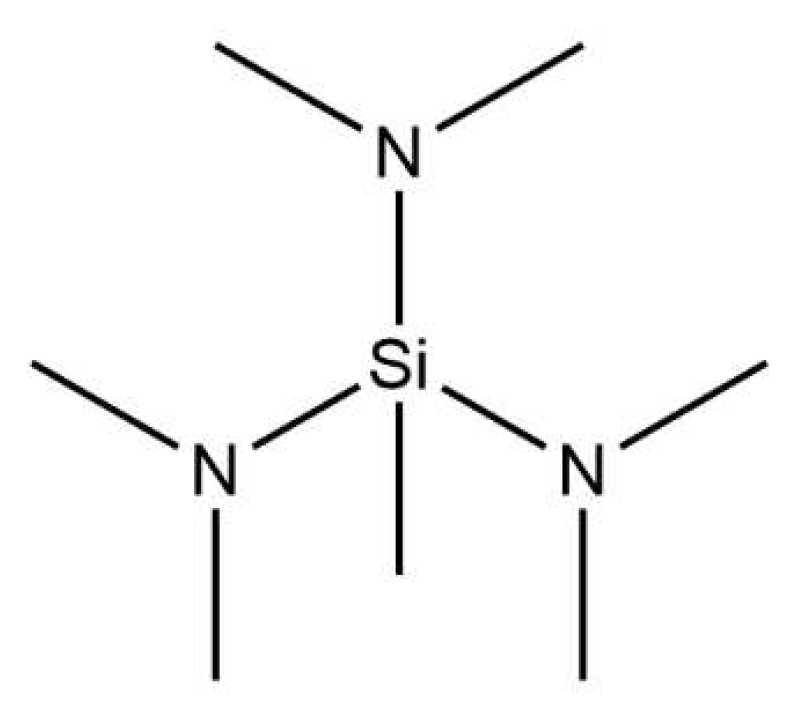
Abstract
1. Introduction
2. Experimental Section
2.1. Materials
2.2. TDMAMS Deposition on Silicon Wafers
2.3. Atomic Layer Deposition (ALD) of ZnO on Passivated Silicon (Si\SiO2)
2.4. Ex Situ Spectroscopic Ellipsometry (SE)
2.5. In Situ Multi-Wavelength Ellipsometry
2.6. X-ray Photoelectron Spectroscopy (XPS)
2.7. High-Sensitivity/Low-Energy Ion Scattering (HS-LEIS)
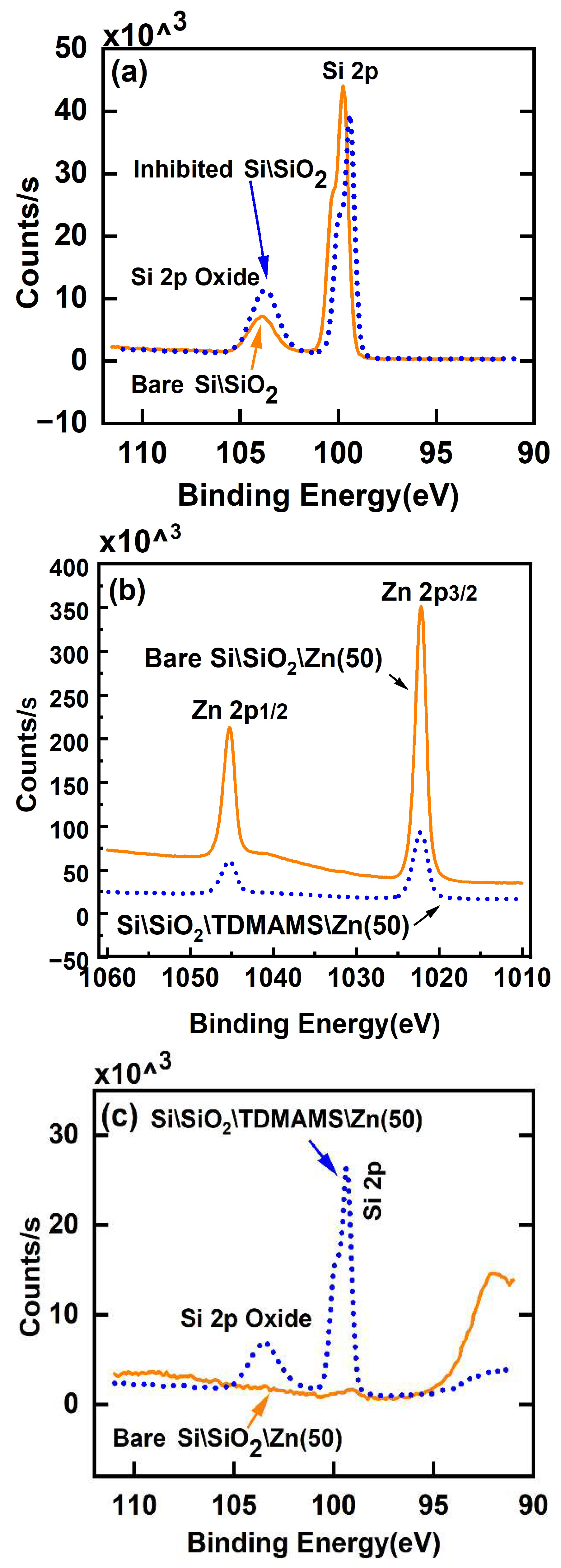
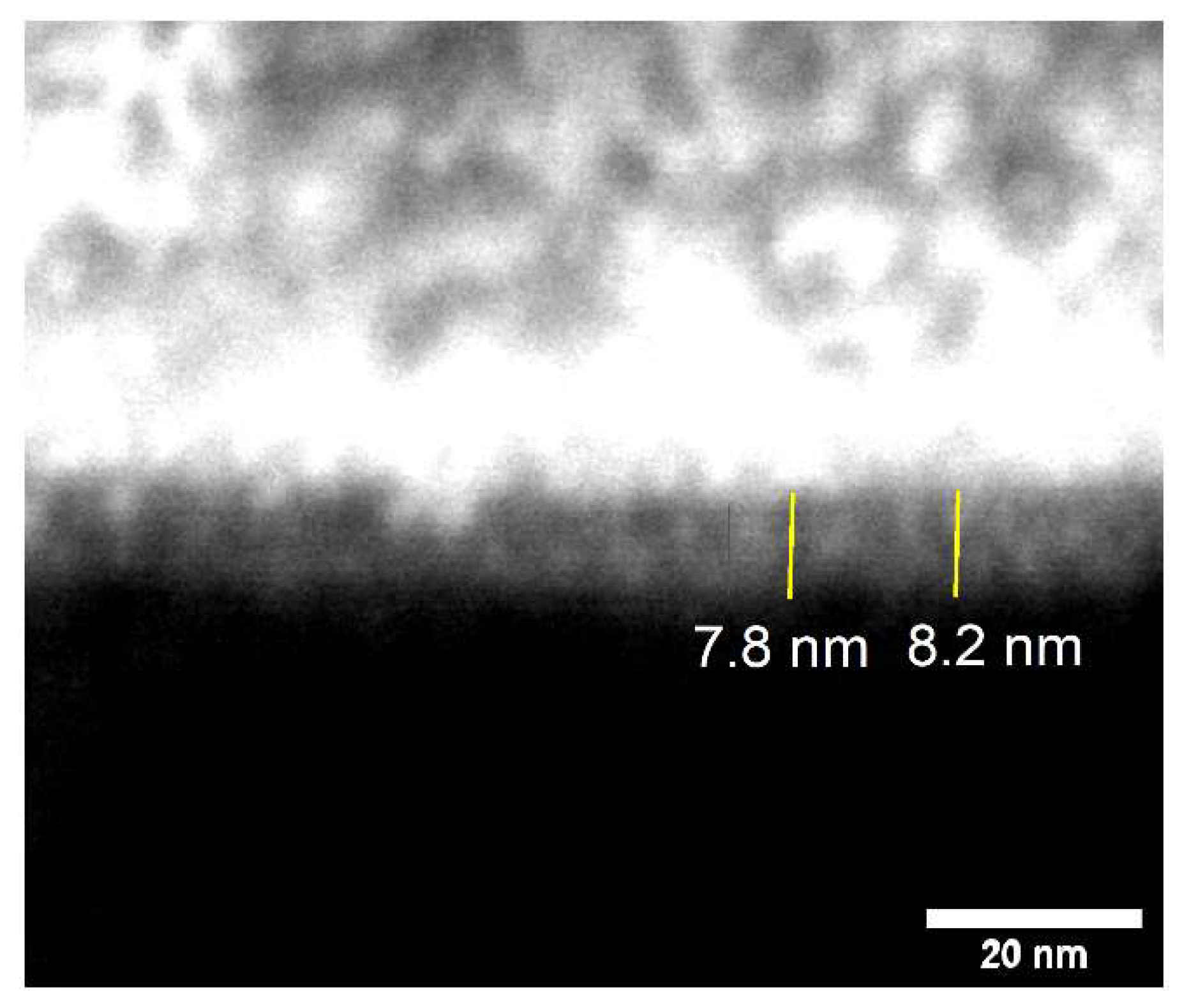
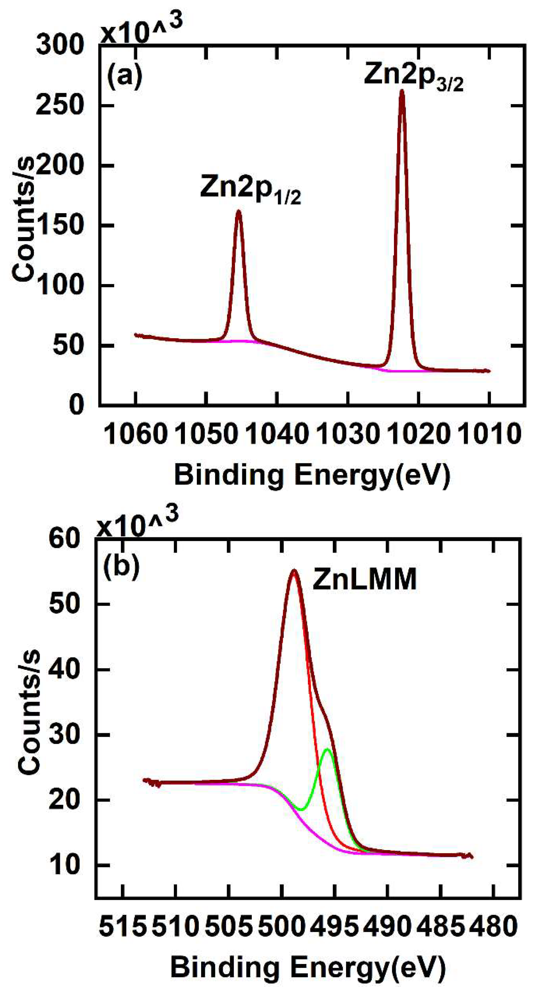
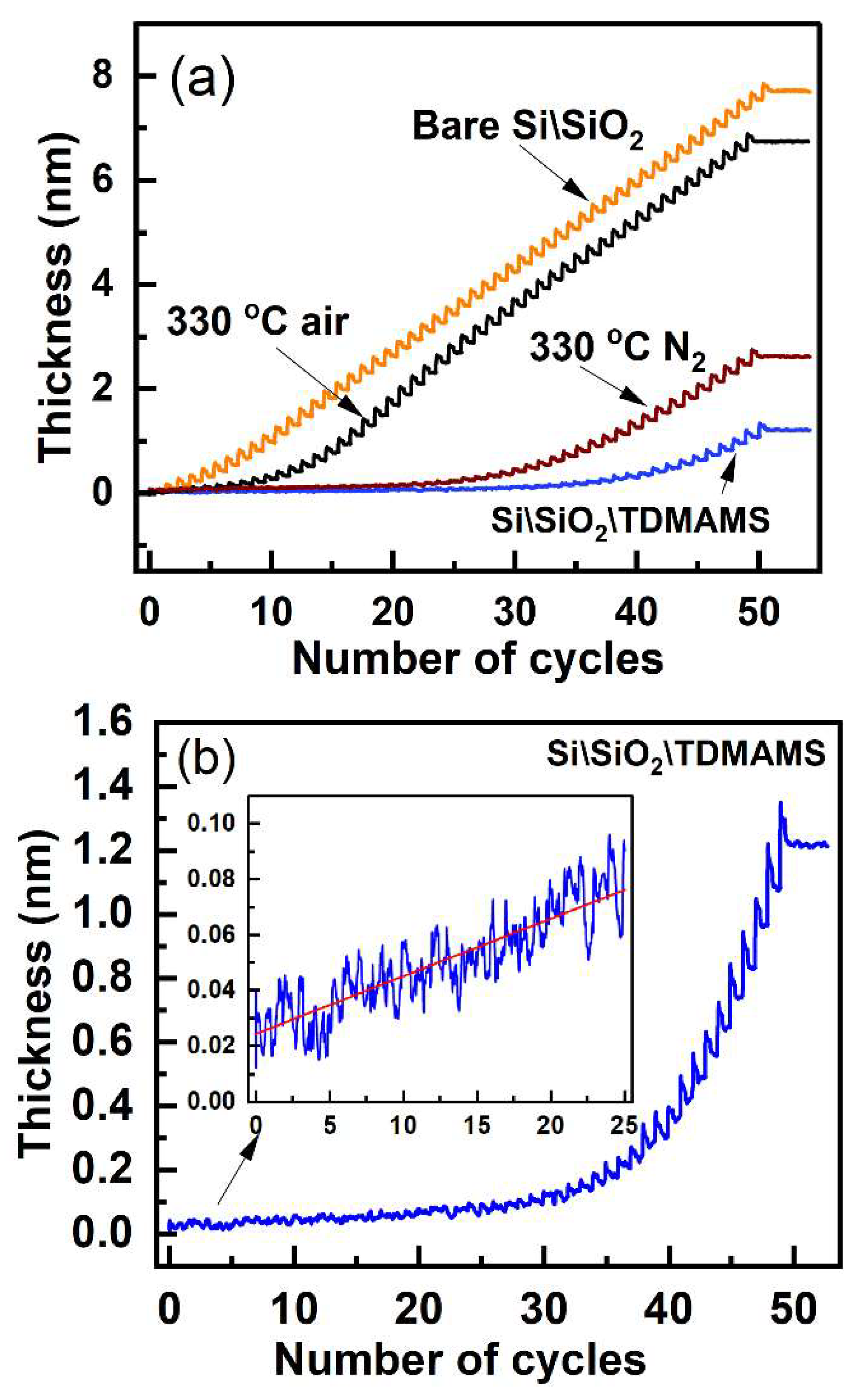
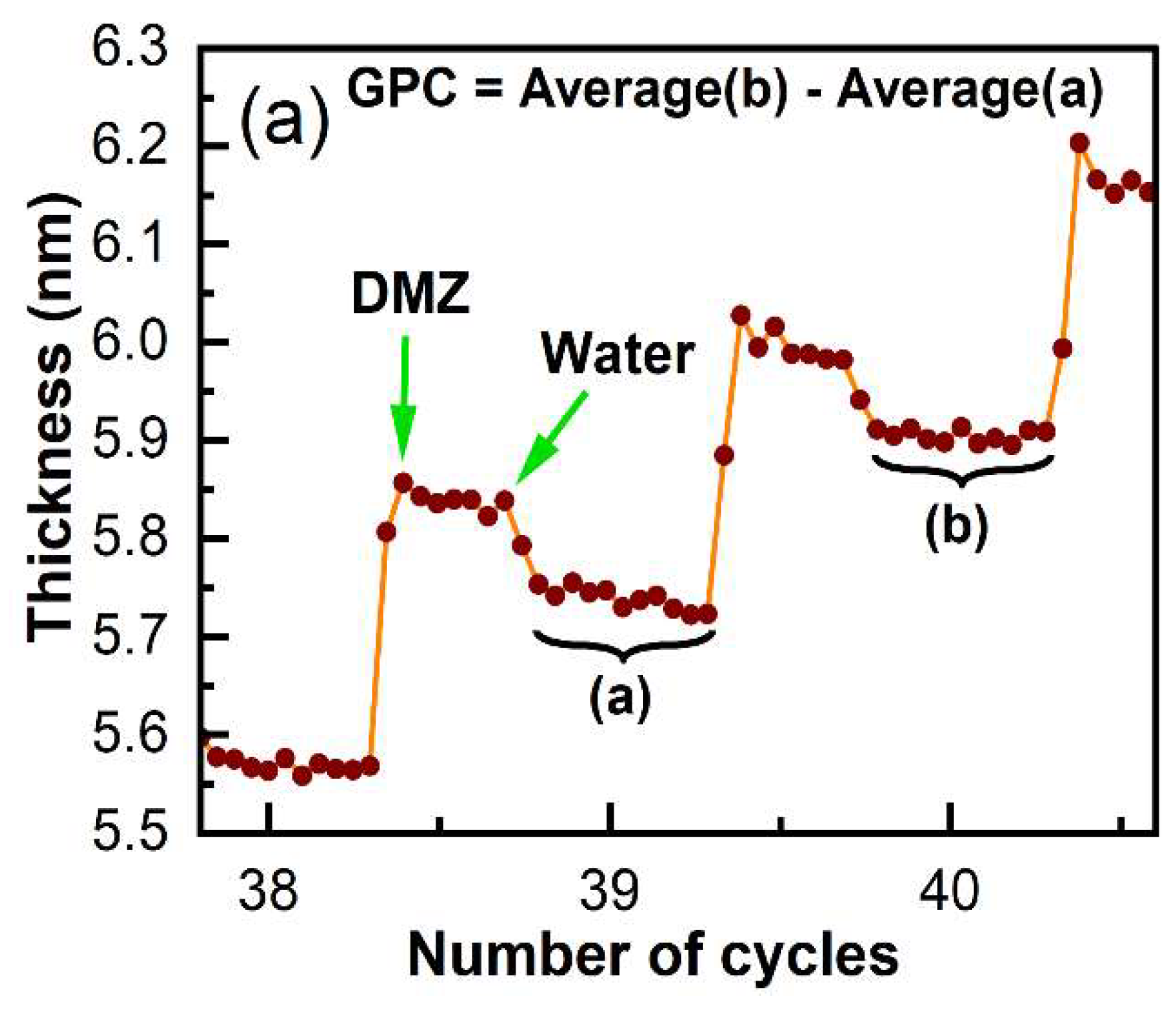
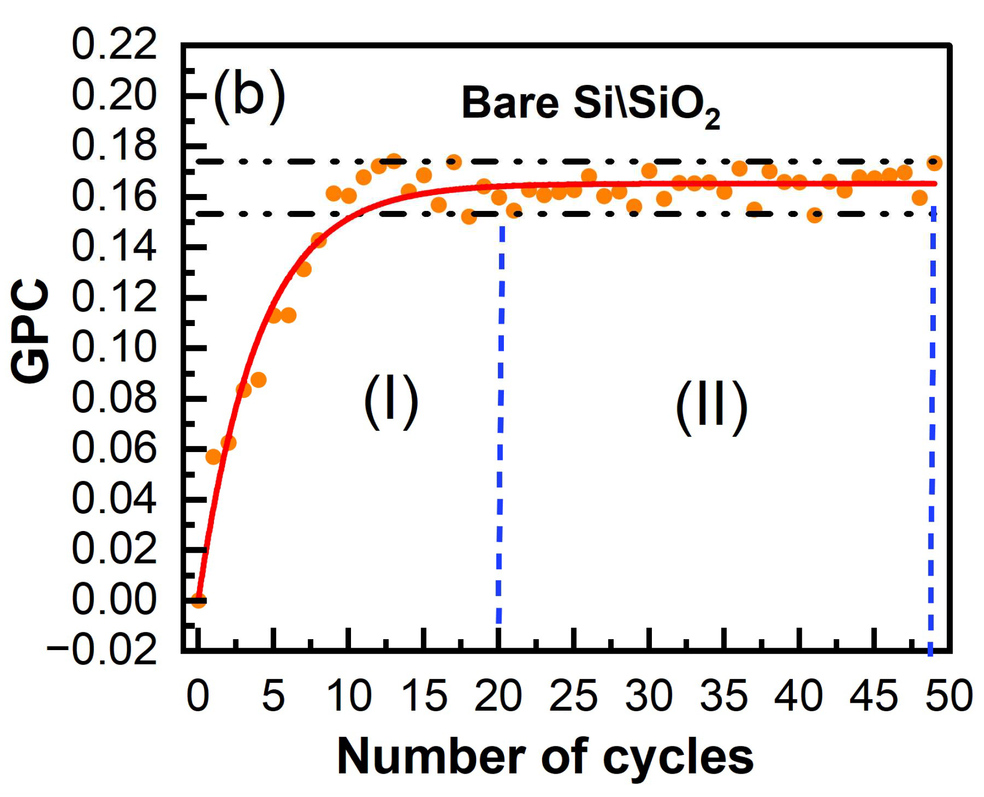
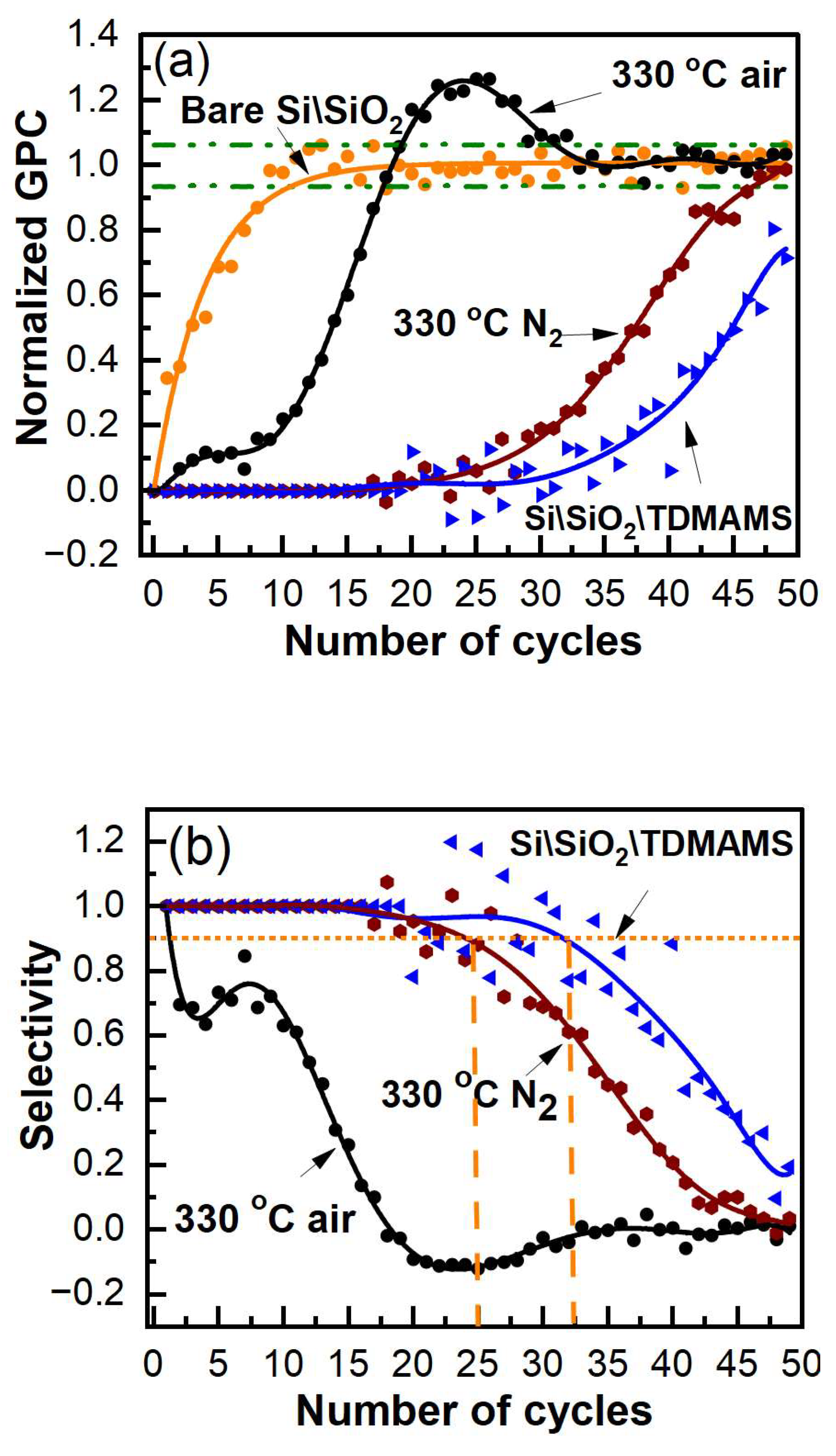
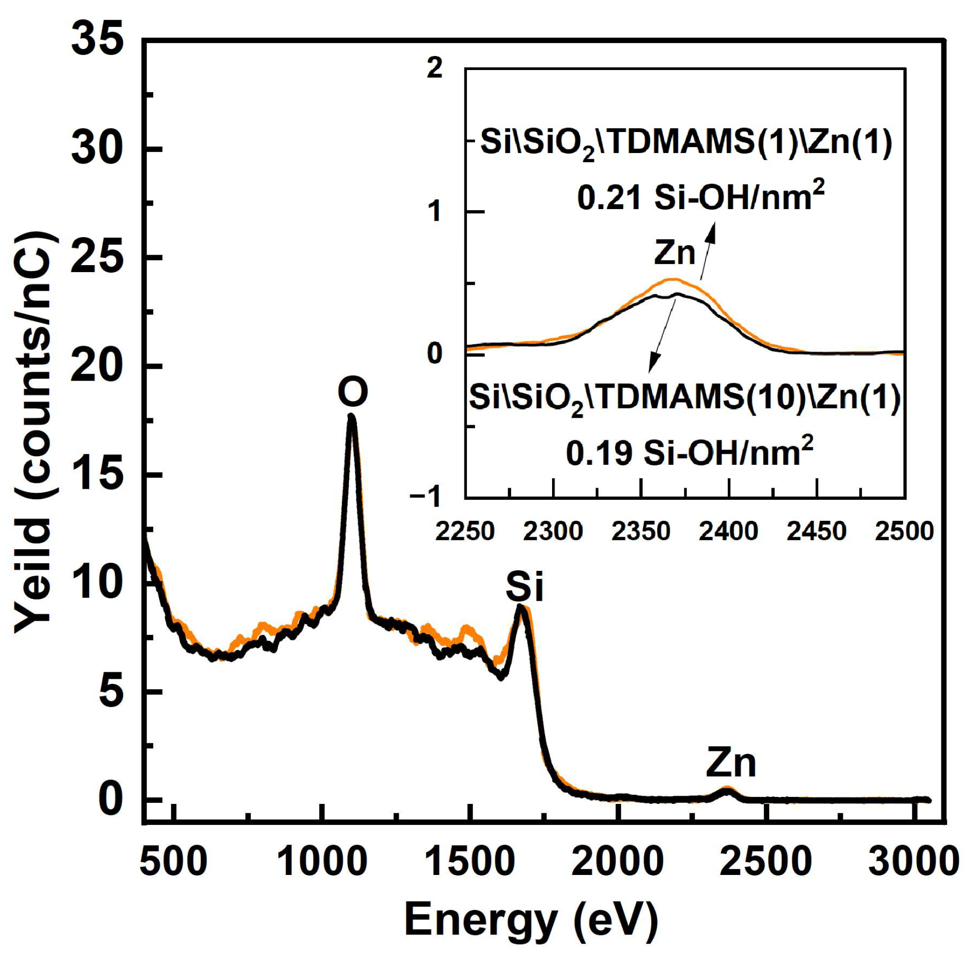
3. Results and Discussion

4. Conclusions
Author Contributions
Funding
Institutional Review Board Statement
Informed Consent Statement
Data Availability Statement
Conflicts of Interest
References
- Puurunen, R.L. A Short History of Atomic Layer Deposition: Tuomo Suntola’s Atomic Layer Epitaxy. Chem. Vap. Depos. 2014, 20, 332–344. [Google Scholar] [CrossRef]
- Kääriäinen, T.; Cameron, D.; Kääriäinen, M.-L.; Sherman, A. Atomic Layer Deposition: Principles, Characteristics, and Nanotechnology Applications; John Wiley & Sons: Hoboken, NJ, USA, 2013. [Google Scholar]
- Mackus, A.J.M.; Merkx, M.J.M.; Kessels, W.M.M. From the Bottom-Up: Toward Area-Selective Atomic Layer Deposition with High Selectivity. Chem. Mater. 2019, 31, 2–12. [Google Scholar] [CrossRef]
- Parsons, G.N.; Clark, R.D. Area-Selective Deposition: Fundamentals, Applications, and Future Outlook. Chem. Mater. 2020, 32, 4920–4953. [Google Scholar] [CrossRef]
- Mameli, A.; Karasulu, B.; Verheijen, M.A.; Mackus, A.J.M.; Kessels, W.M.M.; Roozeboom, F. (Invited) Area-Selective Atomic Layer Deposition: Role of Surface Chemistry. ECS Trans. 2017, 80, 39. [Google Scholar] [CrossRef]
- Chen, R.; Bent, S.F. Chemistry for Positive Pattern Transfer Using Area-Selective Atomic Layer Deposition. Adv. Mater. 2006, 18, 1086–1090. [Google Scholar] [CrossRef]
- Mackus, A.J.M. Approaches and Opportunities for Area-Selective Atomic Layer Deposition. In 2018 International Symposium on VLSI Technology, Systems and Application (VLSI-TSA); IEEE: New York, NY, USA, 2018; pp. 1–2. [Google Scholar] [CrossRef]
- Mameli, A.; Karasulu, B.; Verheijen, M.A.; Barcones, B.; Macco, B.; Mackus, A.J.M.; Kessels, W.M.M.E.; Roozeboom, F. Area-Selective Atomic Layer Deposition of ZnO by Area Activation Using Electron Beam-Induced Deposition. Chem. Mater. 2019, 31, 1250–1257. [Google Scholar] [CrossRef]
- Weber, M.J.; Mackus, A.J.M.; Verheijen, M.A.; van der Marel, C.; Kessels, W.M.M. Supported Core/Shell Bimetallic Nanoparticles Synthesis by Atomic Layer Deposition. Chem. Mater. 2012, 24, 2973–2977. [Google Scholar] [CrossRef]
- Mackus, A.J.M.; Mulders, J.J.L.; Van De Sanden, M.C.M.; Kessels, W.M.M. Local Deposition of High-Purity Pt Nanostructures by Combining Electron Beam Induced Deposition and Atomic Layer Deposition; American Institute of Physics: College Park, MD, USA, 2010. [Google Scholar]
- Chang, C.-W.; Hsu, H.-H.; Hsu, C.-S.; Chen, J.-T. Achieving Area-Selective Atomic Layer Deposition with Fluorinated Self-Assembled Monolayers. J. Mater. Chem. C 2021, 9, 14589–14595. [Google Scholar] [CrossRef]
- Xu, W.; Haeve, M.G.N.; Lemaire, P.C.; Sharma, K.; Hausmann, D.M.; Agarwal, S. Functionalization of the SiO2 Surface with Aminosilanes to Enable Area-Selective Atomic Layer Deposition of Al2O3. Langmuir 2022, 38, 652–660. [Google Scholar] [CrossRef]
- Moeini, B.; Joshua, W.P.; Avval, T.G.; Jacobsen, C.; Brongersma, H.H.; Prusa, S.; Bábík, P.; Vaníčková, E.; Argyle, M.D.; Strohmeier, B.R.; et al. Controlling the Surface Silanol Density in Capillary Columns and Planar Silicon via the Self-Limiting Gas-Phase Deposition of Tris(dimethylamino)Methylsilane, and Quantification of Surface Silanols after Silanization by Low Energy Ion Scattering. 2023. Submitted. [Google Scholar]
- Patel, D.I.; Major, G.H.; Jacobsen, C.; Shah, D.; Strohmeier, B.R.; Shollenberger, D.; Bell, D.S.; Argyle, M.D.; Linford, M.R. Flow-Through Atmospheric Pressure-Atomic Layer Deposition Reactor for Thin-Film Deposition in Capillary Columns. Anal. Chem. 2022, 94, 7483–7491. [Google Scholar] [CrossRef]
- Tonezzer, M.; Dang, T.T.L.; Bazzanella, N.; Nguyen, V.H.; Iannotta, S. Comparative Gas-Sensing Performance of 1D and 2D ZnO Nanostructures. Sens. Actuators B Chem. 2015, 220, 1152–1160. [Google Scholar] [CrossRef]
- Ding, M.; Guo, Z.; Zhou, L.; Fang, X.; Zhang, L.; Zeng, L.; Xie, L.; Zhao, H. One-Dimensional Zinc Oxide Nanomaterials for Application in High-Performance Advanced Optoelectronic Devices. Crystals 2018, 8, 223. [Google Scholar] [CrossRef]
- Sushma, C.; Girish Kumar, S. Advancements in the Zinc Oxide Nanomaterials for Efficient Photocatalysis. Chem. Pap. 2017, 71, 2023–2042. [Google Scholar] [CrossRef]
- Ellmer, K.; Klein, A.; Rech, B. Transparent Conductive Zinc Oxide: Basics and Applications in Thin Film Solar Cells; Springer: Berlin/Heidelberg, Germany, 2007. [Google Scholar]
- Hirao, T.; Furuta, M.; Furuta, H.; Matsuda, T.; Hiramatsu, T.; Hokari, H.; Yoshida, M.; Ishii, H.; Kakegawa, M. Novel Top-gate Zinc Oxide Thin-film Transistors (ZnO TFTs) for AMLCDs. J. Soc. Inf. Disp. 2007, 15, 17–22. [Google Scholar] [CrossRef]
- Guziewicz, E.; Krajewski, T.A.; Przezdziecka, E.; Korona, K.P.; Czechowski, N.; Klopotowski, L.; Terziyska, P. Zinc Oxide Grown by Atomic Layer Deposition: From Heavily n-Type to p-Type Material. Phys. Status Solidi 2020, 257, 1900472. [Google Scholar] [CrossRef]
- Chen, M.-C.; Chang, T.-C.; Tsai, C.-T.; Huang, S.-Y.; Chen, S.-C.; Hu, C.-W.; Sze, S.M.; Tsai, M.-J. Influence of Electrode Material on the Resistive Memory Switching Property of Indium Gallium Zinc Oxide Thin Films. Appl. Phys. Lett. 2010, 96, 262110. [Google Scholar] [CrossRef]
- Parsons, G.N. Functional Model for Analysis of ALD Nucleation and Quantification of Area-Selective Deposition. J. Vac. Sci. Technol. A 2019, 37, 20911. [Google Scholar] [CrossRef]
- Gladfelter, W.L. Selective Metalization by Chemical Vapor Deposition. Chem. Mater. 1993, 5, 1372–1388. [Google Scholar] [CrossRef]
- Longo, R.C.; McDonnell, S.; Dick, D.; Wallace, R.M.; Chabal, Y.J.; Owen, J.H.G.; Ballard, J.B.; Randall, J.N.; Cho, K. Selectivity of Metal Oxide Atomic Layer Deposition on Hydrogen Terminated and Oxidized Si(001)-(2 × 1) Surface. J. Vac. Sci. Technol. B 2014, 32, 03D112. [Google Scholar] [CrossRef]
- Hilfiker, J.N. 5-In Situ Spectroscopic Ellipsometry (SE) for Characterization of Thin Film Growth. In Woodhead Publishing Series in Electronic and Optical Materials; Woodhead Publishing: Cambridge, UK, 2011; pp. 99–151. [Google Scholar] [CrossRef]
- Maynard, H.L.; Layadi, N.; Lee, J.T.C. Plasma Etching of Submicron Devices: In Situ Monitoring and Control by Multi-Wavelength Ellipsometry. Thin Solid Film. 1998, 313–314, 398–405. [Google Scholar] [CrossRef]
- Fang, L.; Li, H.; Ma, X.; Song, Q.; Chen, R. Optical Properties of Ultrathin ZnO Films Fabricated by Atomic Layer Deposition. Appl. Surf. Sci. 2020, 527, 146818. [Google Scholar] [CrossRef]
- Tompkins, H.G. A User’s Guide to Ellipsometry; Courier Corporation: North Chelmsford, MA, USA, 2006. [Google Scholar]
- Jensen, D.S.; Kanyal, S.S.; Madaan, N.; Vail, M.A.; Dadson, A.E.; Engelhard, M.H.; Linford, M.R. Silicon (100)/SiO2 by XPS. Surf. Sci. Spectra 2013, 20, 36–42. [Google Scholar] [CrossRef]
- Biesinger, M.C.; Lau, L.W.M.; Gerson, A.R.; Smart, R.S.C. Resolving Surface Chemical States in XPS Analysis of First Row Transition Metals, Oxides and Hydroxides: Sc, Ti, V, Cu and Zn. Appl. Surf. Sci. 2010, 257, 887–898. [Google Scholar] [CrossRef]
- Wagner, C.D. Chemical Shifts of Auger Lines, and the Auger Parameter. Faraday Discuss. Chem. Soc. 1975, 60, 291–300. [Google Scholar] [CrossRef]
- Wagner, C.D.; Joshi, A. The Auger Parameter, Its Utility and Advantages: A Review. J. Electron Spectros. Relat. Phenom. 1988, 47, 283–313. [Google Scholar] [CrossRef]
- Gaarenstroom, S.W.; Winograd, N. Initial and Final State Effects in the ESCA Spectra of Cadmium and Silver Oxides. J. Chem. Phys. 2008, 67, 3500–3506. [Google Scholar] [CrossRef]
- Ortega, S.; Halicek, M.; Fabelo, H.; Callico, G.M.; Fei, B. Hyperspectral and Multispectral Imaging in Digital and Computational Pathology: A Systematic Review [Invited]. Biomed. Opt. Express 2020, 11, 3195–3233. [Google Scholar] [CrossRef] [PubMed]
- Fairley, N.; Fernandez, V.; Richard-Plouet, M.; Guillot-Deudon, C.; Walton, J.; Smith, E.; Flahaut, D.; Greiner, M.; Biesinger, M.; Tougaard, S.; et al. Systematic and Collaborative Approach to Problem Solving Using X-Ray Photoelectron Spectroscopy. Appl. Surf. Sci. Adv. 2021, 5, 100112. [Google Scholar] [CrossRef]
- Hesse, R.; Streubel, P.; Szargan, R. Product or Sum: Comparative Tests of Voigt, and Product or Sum of Gaussian and Lorentzian Functions in the Fitting of Synthetic Voigt-Based X-Ray Photoelectron Spectra. Surf. Interface Anal. 2007, 39, 381–391. [Google Scholar] [CrossRef]
- Dake, L.S.; Baer, D.R.; Zachara, J.M. Auger Parameter Measurements of Zinc Compounds Relevant to Zinc Transport in the Environment. Surf. Interface Anal. 1989, 14, 71–75. [Google Scholar] [CrossRef]
- Collins, T.J. ImageJ for Microscopy. Biotechniques 2007, 43, S25–S30. [Google Scholar] [CrossRef] [PubMed]


Disclaimer/Publisher’s Note: The statements, opinions and data contained in all publications are solely those of the individual author(s) and contributor(s) and not of MDPI and/or the editor(s). MDPI and/or the editor(s) disclaim responsibility for any injury to people or property resulting from any ideas, methods, instructions or products referred to in the content. |
© 2023 by the authors. Licensee MDPI, Basel, Switzerland. This article is an open access article distributed under the terms and conditions of the Creative Commons Attribution (CC BY) license (https://creativecommons.org/licenses/by/4.0/).
Share and Cite
Moeini, B.; Avval, T.G.; Brongersma, H.H.; Průša, S.; Bábík, P.; Vaníčková, E.; Strohmeier, B.R.; Bell, D.S.; Eggett, D.; George, S.M.; et al. Area-Selective Atomic Layer Deposition of ZnO on Si\SiO2 Modified with Tris(dimethylamino)methylsilane. Materials 2023, 16, 4688. https://doi.org/10.3390/ma16134688
Moeini B, Avval TG, Brongersma HH, Průša S, Bábík P, Vaníčková E, Strohmeier BR, Bell DS, Eggett D, George SM, et al. Area-Selective Atomic Layer Deposition of ZnO on Si\SiO2 Modified with Tris(dimethylamino)methylsilane. Materials. 2023; 16(13):4688. https://doi.org/10.3390/ma16134688
Chicago/Turabian StyleMoeini, Behnam, Tahereh G. Avval, Hidde H. Brongersma, Stanislav Průša, Pavel Bábík, Elena Vaníčková, Brian R. Strohmeier, David S. Bell, Dennis Eggett, Steven M. George, and et al. 2023. "Area-Selective Atomic Layer Deposition of ZnO on Si\SiO2 Modified with Tris(dimethylamino)methylsilane" Materials 16, no. 13: 4688. https://doi.org/10.3390/ma16134688
APA StyleMoeini, B., Avval, T. G., Brongersma, H. H., Průša, S., Bábík, P., Vaníčková, E., Strohmeier, B. R., Bell, D. S., Eggett, D., George, S. M., & Linford, M. R. (2023). Area-Selective Atomic Layer Deposition of ZnO on Si\SiO2 Modified with Tris(dimethylamino)methylsilane. Materials, 16(13), 4688. https://doi.org/10.3390/ma16134688