


Investigation of the Performance of Perovskite Solar Cells with ZnO-Covered PC61BM Electron Transport Layer


Abstract
1. Introduction
2. Materials and Methods
2.1. Materials
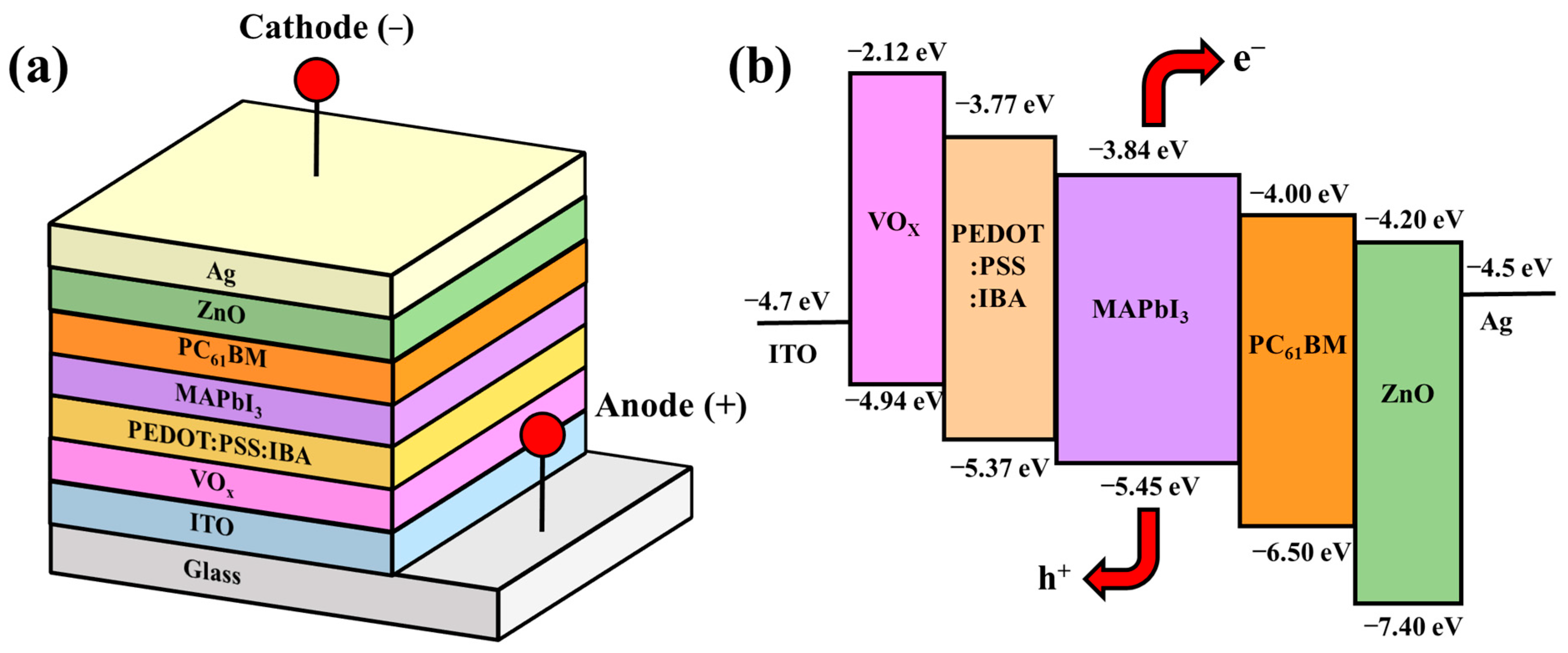
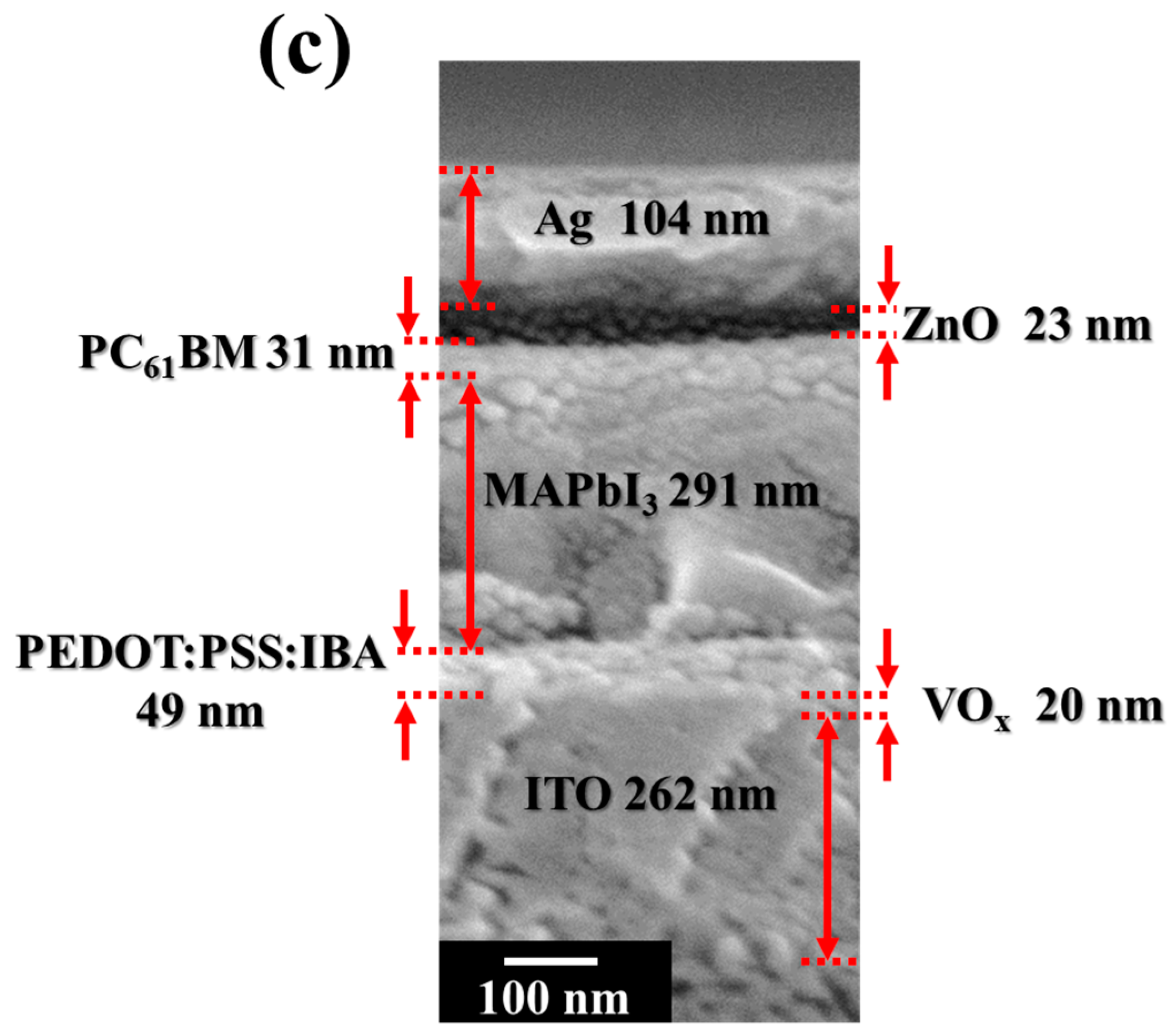
2.2. Manufacture
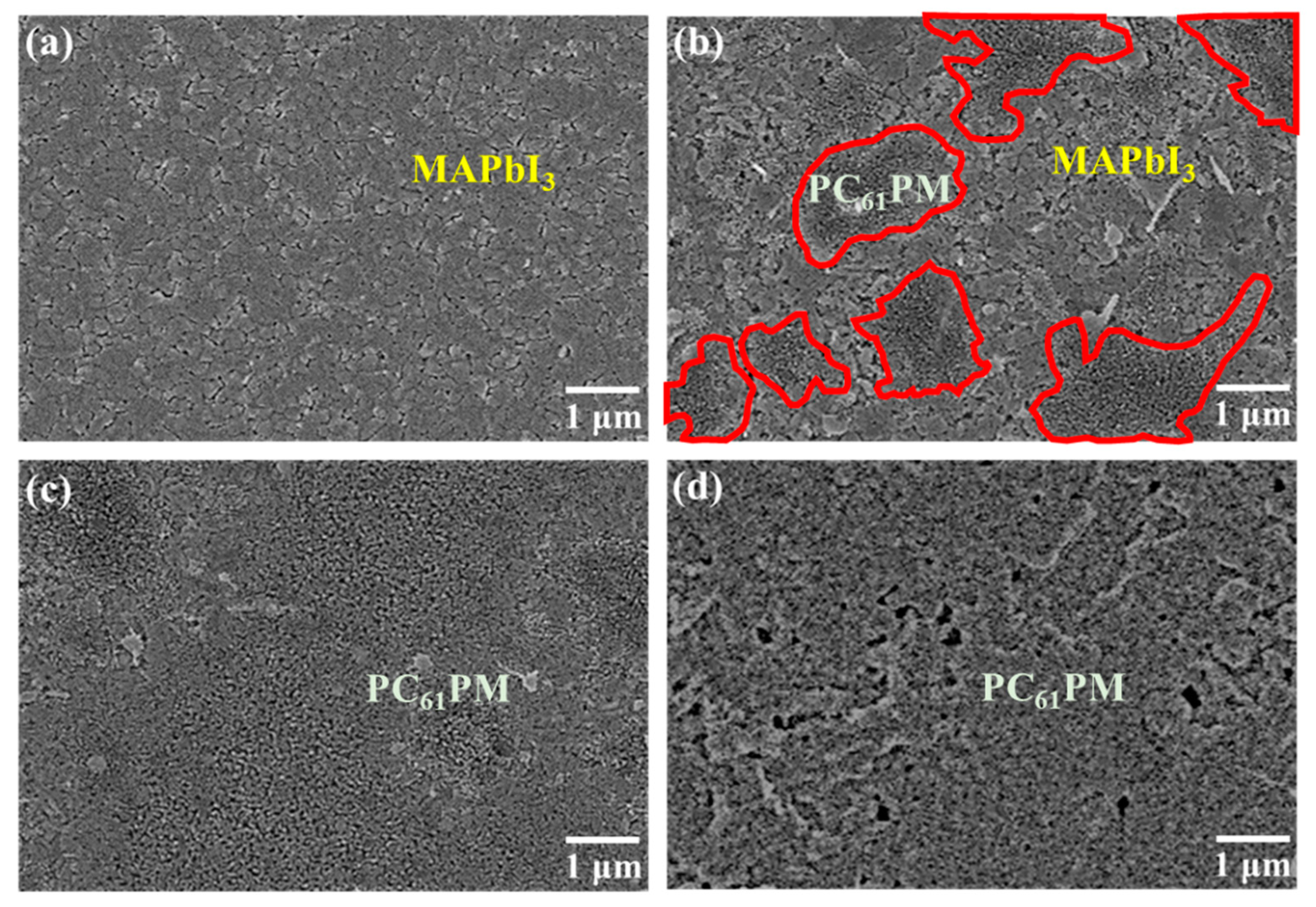
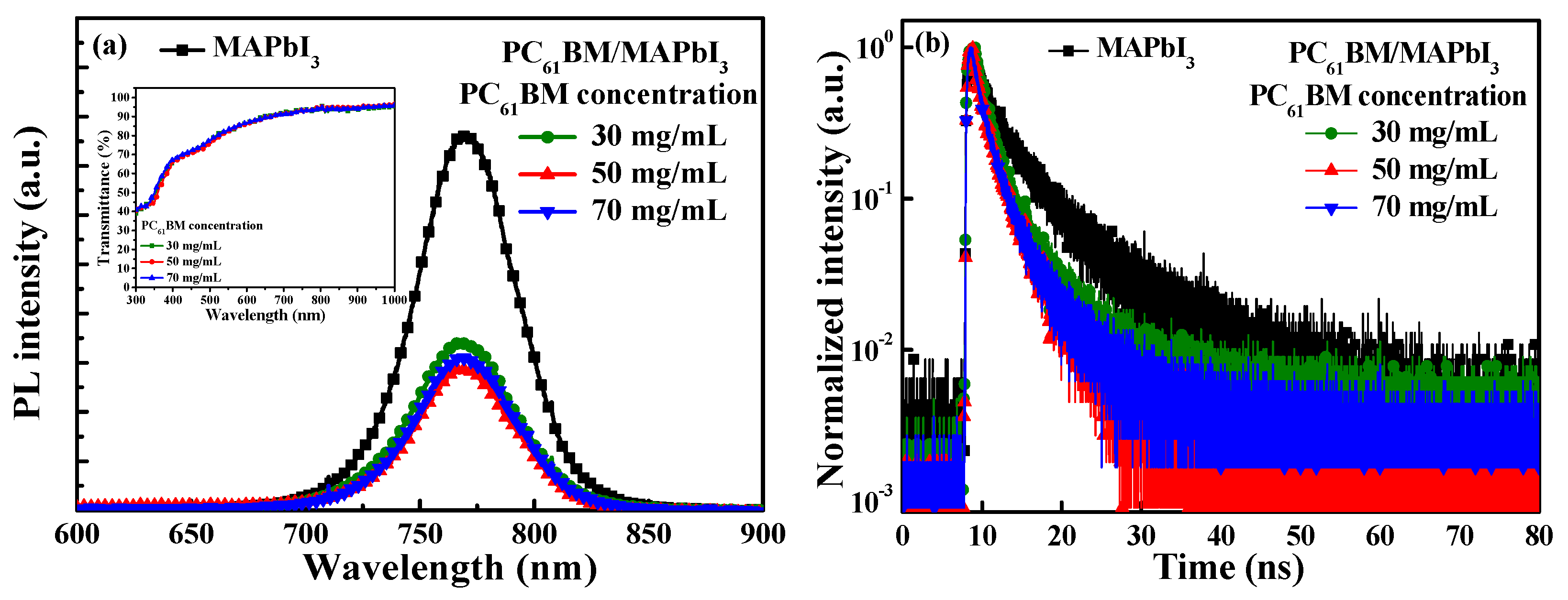
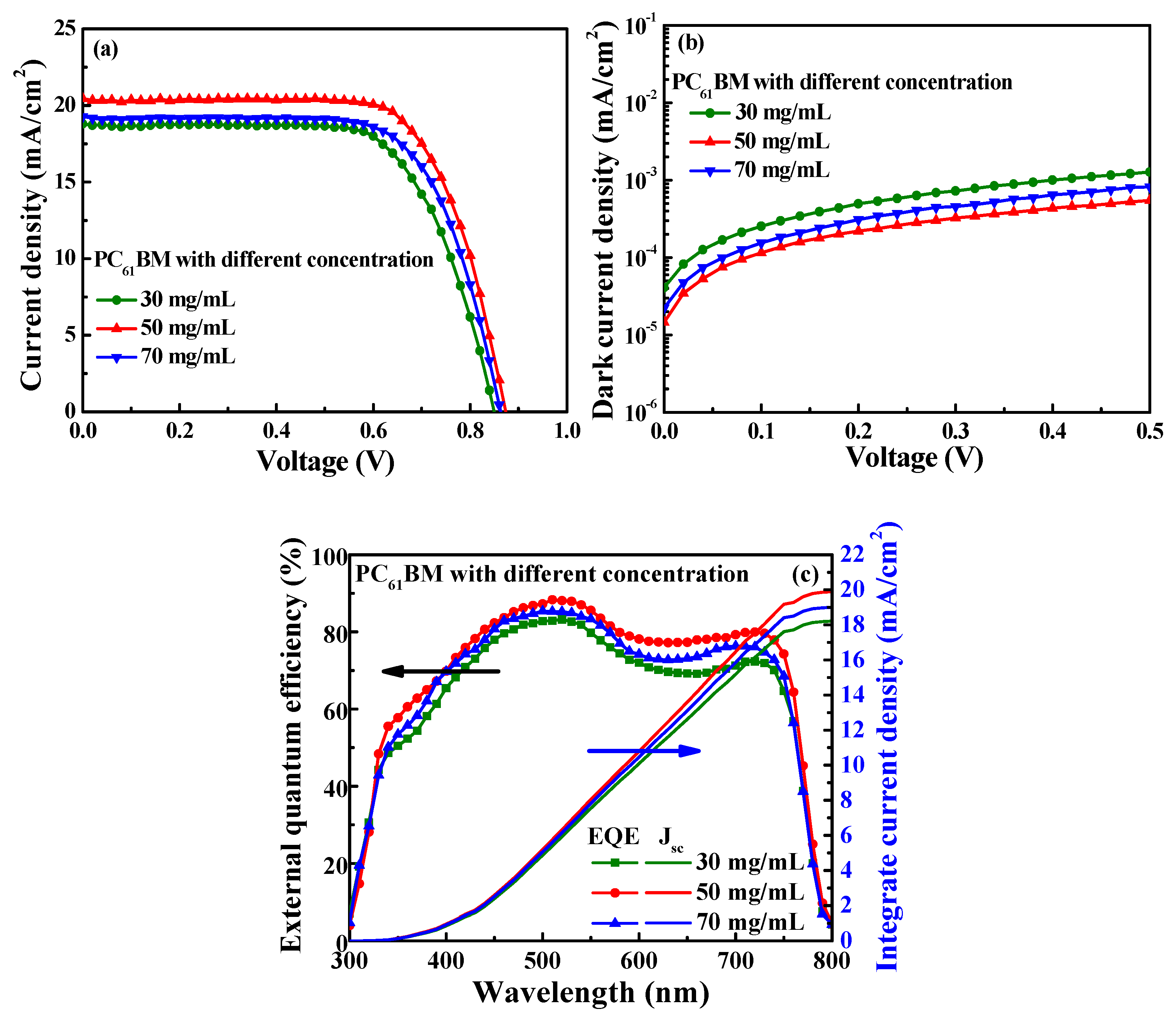
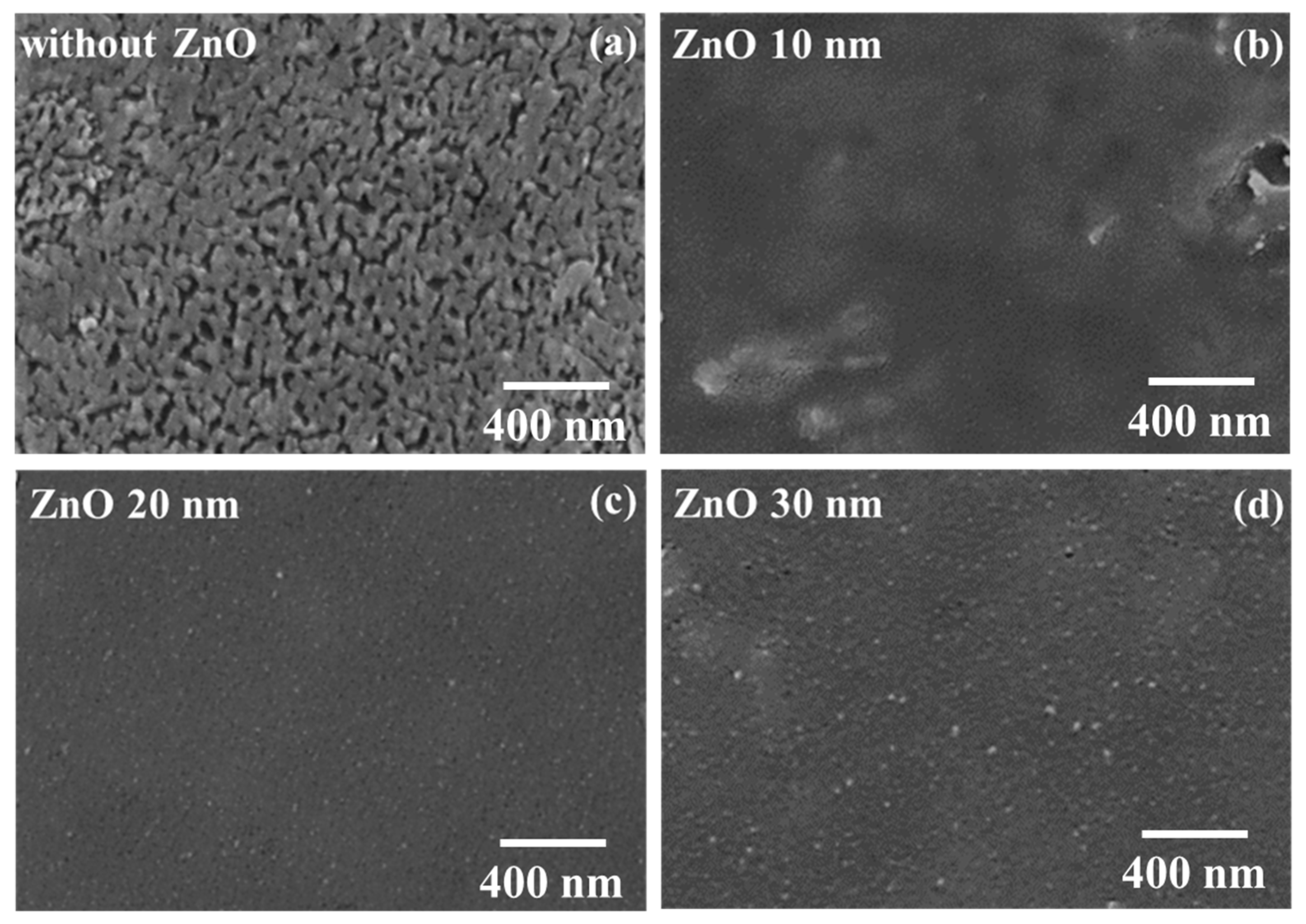
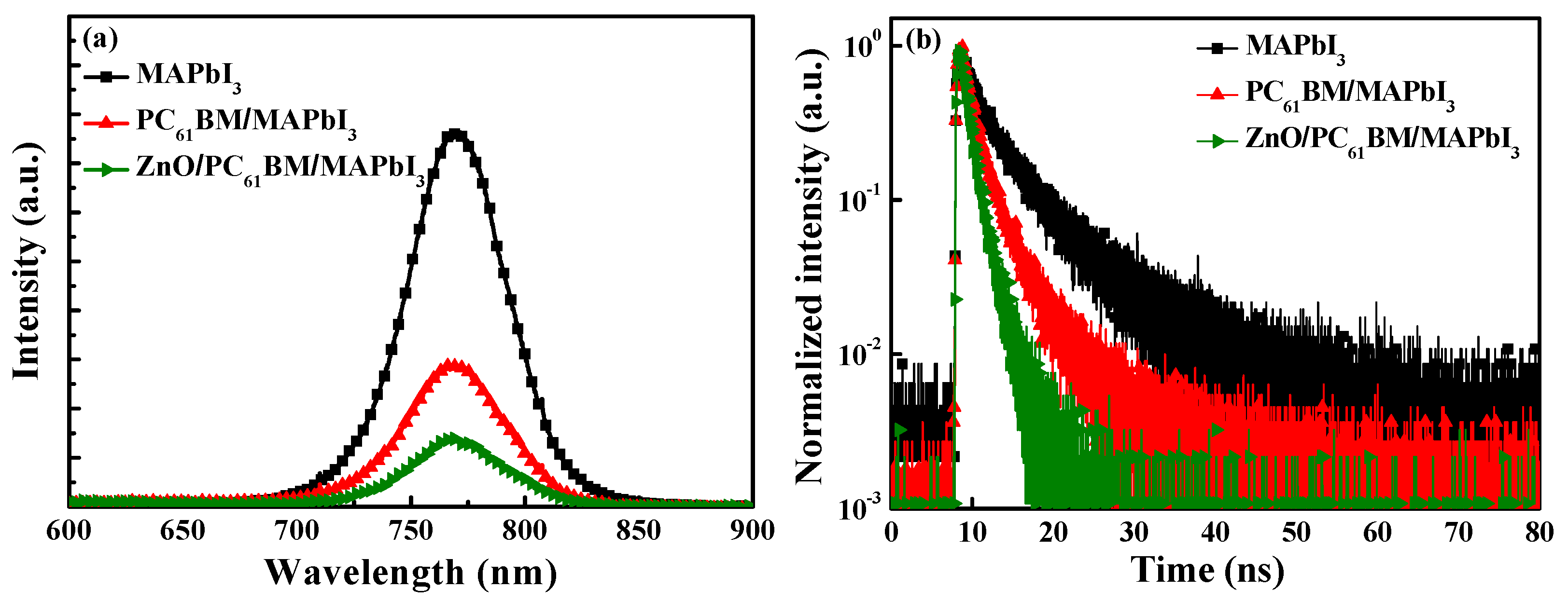
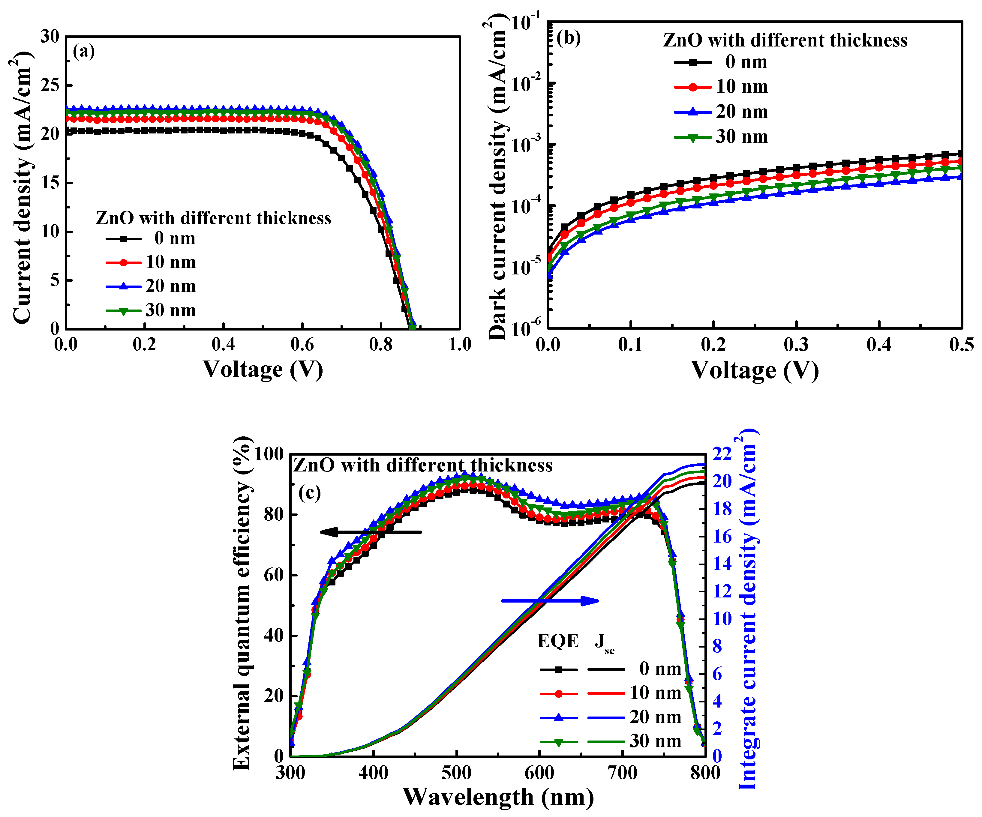
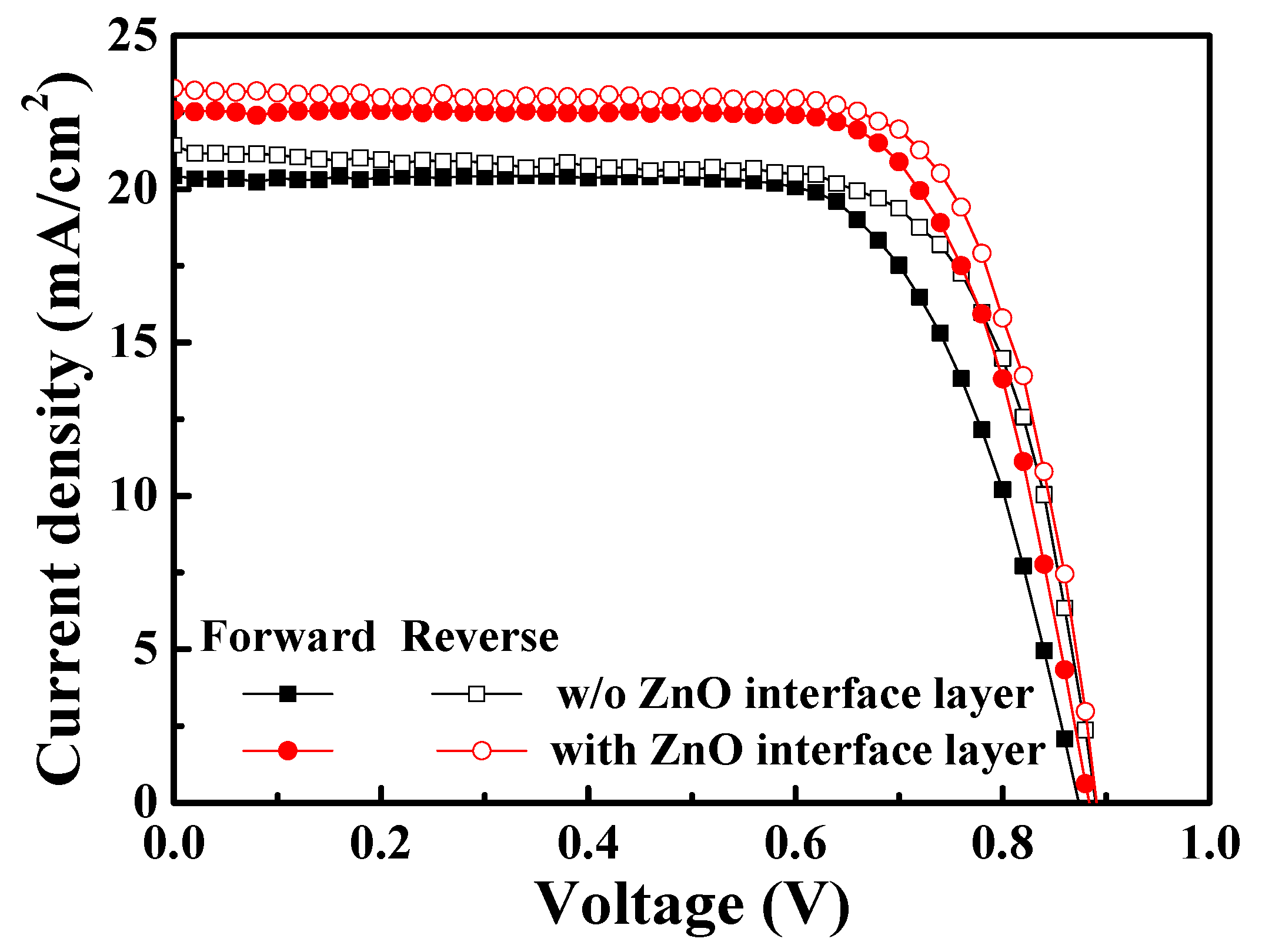
3. Results
4. Conclusions
Author Contributions
Funding
Institutional Review Board Statement
Informed Consent Statement
Data Availability Statement
Conflicts of Interest
References
- Barnham, K.W.J.; Mazzer, M.; Clive, B. Resolving the energy crisis: Nuclear or photovoltaics. Nat. Mater. 2006, 5, 161–164. [Google Scholar] [CrossRef]
- Azar, C.; Lindgren, K.; Andersson, B.A. Global energy scenarios meeting stringent CO2 constraints-cost-effective fuel choices in the transportation sector. Energy Policy 2003, 31, 961–976. [Google Scholar] [CrossRef]
- Fukuda, K.; Yu, K.; Someya, T. The future of flexible organic solar cells. Adv. Energy Mater. 2020, 10, 2000765. [Google Scholar] [CrossRef]
- Lee, H.Y.; Huang, H.L.; Lee, C.T. Performance enhancement of inverted polymer solar cells using roughened Al-doped ZnO nanorod array. Appl. Phys. Express 2012, 5, 122302. [Google Scholar] [CrossRef]
- Ryu, K.; Lee, Y.J.; Ju, M.; Choi, H.; Kim, B.; Lee, J.; Oh, W.; Choi, K.; Balaji, N.; Yi, J. Optimal indium tin oxide layer as antireflection coating for crystalline silicon solar cell with shallow emitter. Thin Solid Films 2012, 521, 50–53. [Google Scholar] [CrossRef]
- Ren, Q.; Li, S.; Zhu, S.; Ren, H.; Yao, X.; Wei, C.; Yan, B.; Zhao, Y.; Zhang, X. High near-infrared wavelength response planar silicon-heterojunction solar cells. Sol. Energy Mater. Sol. Cells 2018, 185, 124–129. [Google Scholar] [CrossRef]
- Yuan, T.; Li, J.; Wang, S. Composited film of poly(3,4-ethylenedioxythiophene) and graphene oxide as hole transport layer in perovskite solar cells. Polymers 2021, 13, 3895. [Google Scholar] [CrossRef]
- Liu, G.Z.; Du, C.S.; Wu, J.Y.; Liu, B.T.; Wu, T.M.; Huang, C.F.; Lee, R.H. Enhanced photovoltaic properties of perovskite solar cells by employing bathocuproine/hydrophobic polymer films as hole-blocking/electron-transporting interfacial layers. Polymers 2021, 13, 42. [Google Scholar] [CrossRef]
- Xu, Y.; Niu, Q.; Zhang, L.; Yuan, C.; Ma, Y.; Hua, W.; Zeng, W.; Min, Y.; Huang, J.; Xia, R. Highly efficient perovskite solar cell based on PVK hole transport layer. Polymers 2022, 14, 2249. [Google Scholar] [CrossRef]
- Larciprete, R.; Agresti, A.; Pescetelli, S.; Pazniak, H.; Liedl, A.; Lacovig, P.; Lizzit, D.; Tosi, E.; Lizzit, S.; Carlo, A.D. Mixed cation halide perovskite under environmental and physical stress. Materials 2021, 14, 3954. [Google Scholar] [CrossRef]
- Kirui, J.K.; Olaleru, S.A.; Jhamba, L.; Wamwangi, D.; Roro, K.; Shnier, A.; Erasmus, R.; Mwakikunga, B. Elucidating the trajectory of the charge transfer mechanism and recombination process of hybrid perovskite solar cells. Materials 2021, 14, 2698. [Google Scholar] [CrossRef]
- Afzal, A.M.; Bae, I.G.; Aggarwal, Y.; Park, J.; Jeong, H.R.; Choi, E.H.; Park, B. Highly efficient self-powered perovskite photodiode with an electron-blocking hole-transport NiOx layer. Sci. Rep. 2021, 11, 169. [Google Scholar] [CrossRef] [PubMed]
- Xing, G.; Mathews, N.; Sun, S.; Lim, S.S.; Lam, Y.M.; Graẗzel, M.; Mhaisalkar, S.; Sum, T.C. Long-range balanced electron-and hole-transport lengths in organic-inorganic CH3NH3PbI3. Science 2013, 342, 344–347. [Google Scholar] [CrossRef]
- Li, L.; Jacobs, D.L.; Che, Y.; Huang, H.; Bunes, B.R.; Yang, X.; Zang, L. Poly(3-hexylthiophene) nanofiber networks for enhancing the morphology stability of polymer solar cells. Org. Electron. 2013, 14, 1383–1390. [Google Scholar] [CrossRef]
- Wang, H.; Wang, Y.; Xuan, Z.; Chen, T.; Zhang, J.; Hao, X.; Wu, L.; Constantinou, I.; Zhao, D. Progress in perovskite solar cells towards commercialization—A review. Materials 2021, 14, 6569. [Google Scholar] [CrossRef]
- Kamaraki, C.; Zachariadis, A.; Kapnopoulos, C.; Mekeridis, E.; Gravalidis, C.; Laskarakis, A.; Logothetidis, S. Efficient flexible printed perovskite solar cells based on lead acetate precursor. Sol. Energy 2018, 176, 406–411. [Google Scholar] [CrossRef]
- Chen, C.; Zhai, Y.; Li, F.; Tan, F.; Yue, G.; Zhang, W.; Wang, M. High efficiency CH3NH3PbI3:CdS perovskite solar cells with CuInS2 as the hole transporting layer. J. Power Sources 2017, 341, 396–403. [Google Scholar] [CrossRef]
- Liu, Z.; Xie, X.; Liu, G.; Lee, E.C. High-performance metal-oxide-free perovskite solar cells based on organic electron transport layer and cathode. Org. Electron. 2019, 64, 195–201. [Google Scholar] [CrossRef]
- Fu, Y.; Song, Q.; Lin, T.; Wang, Y.; Sun, X.; Su, Z.; Chu, B.; Jin, F.; Zhao, H.; Li, W.; et al. High performance photomultiplication perovskite photodetectors with PC60BM and NPB as the interlayers. Org. Electron. 2017, 51, 200–206. [Google Scholar] [CrossRef]
- Kim, B.J.; Kim, D.H.; Lee, Y.Y.; Shin, H.W.; Han, G.S.; Hong, J.S.; Mahmood, K.; Ahn, T.K.; Joo, Y.C.; Hong, K.S.; et al. Highly efficient and bending durable perovskite solar cells: Toward a wearable power source. Energy Environ. Sci. 2015, 8, 916–921. [Google Scholar] [CrossRef]
- Tao, C.; Neutzner, S.; Colella, L.; Marras, S.; Kandada, A.R.S.; Gandini, M.; Bastiani, M.D.; Pace, G.; Manna, L.; Caironi, M.; et al. 17.6% stabilized efficiency in low-temperature processed planar perovskite solar cells. Energy Environ. Sci. 2015, 8, 2365–2370. [Google Scholar] [CrossRef]
- Lee, K.; Ryu, J.; Yu, H.; Yun, J.; Lee, J.; Jang, J. Enhanced efficiency and air-stability of NiOx-based perovskite solar cells via PCBM electron transport layer modification with Triton X-100. Nanoscale 2017, 9, 16249–16255. [Google Scholar] [CrossRef] [PubMed]
- Jiu, T.; Li, Y.; Li, Y. New method for the synthesis of a highly-conjugated acene material and its application in perovskite solar cells. Mater. Chem. Front. 2017, 1, 2261–2264. [Google Scholar] [CrossRef]
- Kuang, C.; Tang, G.; Jiu, T.; Yang, H.; Liu, H.; Li, B.; Luo, W.; Li, X.; Zhang, W.; Lu, F.; et al. Highly efficient electron transport obtained by doping PCBM with graphdiyne in planar-heterojunction perovskite solar cells. Nano Lett. 2015, 15, 2756–2762. [Google Scholar] [CrossRef]
- Tsai, J.H.; Tsai, M.C.; Sung, C.Y.; Huang, P.T. Significant increase in current density of inverted polymer solar cells by induced-crystallization of sol-gel ZnO embedded with ZnO-NP. Org. Electron. 2020, 86, 105891. [Google Scholar] [CrossRef]
- Luo, J.; Wang, Y.; Zhang, Q. Progress in perovskite solar cells based on ZnO nanostructures. Sol. Energy 2018, 163, 289–306. [Google Scholar] [CrossRef]
- You, J.; Meng, L.; Song, T.B.; Guo, T.F.; Yang, Y.M.; Chang, W.H.; Hong, Z.; Chen, H.; Zhou, H.; Chen, Q.; et al. Improved air stability of perovskite solar cells via solution-processed metal oxide transport layers. Nat. Nanotechnol. 2016, 11, 75–81. [Google Scholar] [CrossRef]
- Yeh, T.H.; Lee, H.Y.; Lee, C.T. Performance improvement of perovskite solar cells using vanadium oxide interface modification layer. J. Alloys Compd. 2020, 822, 153620. [Google Scholar] [CrossRef]
- Götz, A.W.; Rodríguez, J.I.; Castillo-Alvarado, F.L.; Trujillo-González, D.E. Van der Waals effects on structure and optical propertiesin organic photovoltaics. Int. J. Quantum Chem. 2019, 119, e25883. [Google Scholar] [CrossRef]
- Sutthana, S.; Hongsith, K.; Ruankham, P.; Wongratanaphisan, D.; Gardchareon, A.; Phadungdhitidhada, S.; Boonyawan, D.; Kumnorkaew, P.; Tuantranont, A.; Choopun, S. Interface modification of CH3NH3PbI3/PCBM by pre-heat treatment for efficiency enhancement of perovskite solar cells. Curr. Appl. Phys. 2007, 17, 488–494. [Google Scholar] [CrossRef]
- Baranowski, M.; Kudrawiec, R.; Syperek, M.; Misiewicz, J.; Sarmiento, T.; Harris, J.S. Time-resolved photoluminescence studies of annealed 1.3-μm GaInNAsSb quantum wells. Nanoscale Res. Lett. 2014, 9, 81. [Google Scholar] [CrossRef] [PubMed]
- Chen, P.S.; Lee, T.H.; Lai, L.W.; Lee, C.T. Schottky mechanism for Ni/Au contact with chlorine-treated n-type GaN layer. J. Appl. Phys. 2007, 101, 024507. [Google Scholar] [CrossRef]
- Lai, L.W.; Lee, C.T. Investigation of optical and electrical properties of ZnO thin films. Mater. Chem. Phys. 2008, 110, 393–396. [Google Scholar] [CrossRef]
- Huang, J.; Yu, X.; Xie, J.; Li, C.Z.; Zhang, Y.; Xu, D.; Tang, Z.; Cui, C.; Yang, D. Fulleropyrrolidinium iodide as an efficient electron transport layer for air-stable planar perovskite solar cells. ACS Appl. Mater. Interfaces 2016, 8, 34612–34619. [Google Scholar] [CrossRef]
- Svanstrom, S.; Jacobsson, T.J.; Boschloo, G.; Johansson, E.M.J.; Rensmo, H.; Cappel, U.B. Degradation mechanism of silver metal deposited on lead halide perovskites. ACS Appl. Mater. Interfaces 2020, 12, 7212–7221. [Google Scholar] [CrossRef] [PubMed]
- Park, S.; Jang, W.; Wang, D.H. Alignment of cascaded band-gap via PCBM/ZnO hybrid interlayers for efficient perovskite photovoltaic cells. Macromol. Res. 2018, 26, 472–476. [Google Scholar] [CrossRef]
- Lee, H.J.; Na, S.I. Investigation of PCBM/ZnO and C60/BCP-based electron transport layer for high-performance p-i-n perovskite solar cells. J. Alloys Compd. 2022, 921, 166007. [Google Scholar] [CrossRef]
- Habisreutinger, S.N.; Noel, N.K.; Snaith, H.J. Hysteresis index: A figure without merit for quantifying hysteresis in perovskite solar cells. ACS Energy Lett. 2018, 3, 2472–2476. [Google Scholar] [CrossRef]
- Jiang, H.; Jiang, G.; Xing, W.; Xiong, W.; Zhang, X.; Wang, B.; Zhang, H.; Zheng, Y. High current density and low hysteresis effect of planar perovskite solar cells via PCBM-doping and interfacial improvement. ACS Appl. Mater. Interfaces 2018, 10, 29954–29964. [Google Scholar] [CrossRef]


| PC61BM Concentration (mg/mL) | Voc (V) | Jsc (mA/cm2) | FF (%) | PCE (%) | Integrated Jsc (mA/cm2) |
|---|---|---|---|---|---|
| 30 | 0.85 | 18.79 | 67.81 | 10.83 | 18.22 |
| 50 | 0.87 | 20.44 | 70.52 | 12.54 | 19.89 |
| 70 | 0.86 | 19.28 | 69.48 | 11.52 | 19.00 |
| ZnO Thickness (nm) | Voc (V) | Jsc (mA/cm2) | FF (%) | PCE (%) | Integrated Jsc (mA/cm2) |
|---|---|---|---|---|---|
| 0 | 0.87 | 20.44 | 70.52 | 12.54 | 19.89 |
| 10 | 0.88 | 21.62 | 72.74 | 13.84 | 20.33 |
| 20 | 0.88 | 22.57 | 73.61 | 14.62 | 21.26 |
| 30 | 0.88 | 22.29 | 73.51 | 14.42 | 20.75 |
| Structure (Scan Direction) | Voc (V) | Jsc (mA/cm2) | FF (%) | PCE (%) | Hysteresis Index (%) |
|---|---|---|---|---|---|
| Without ZnO (Forward) | 0.87 | 20.44 | 70.52 | 12.54 | 7.52 |
| Without ZnO (Reverse) | 0.89 | 21.43 | 71.10 | 13.56 | |
| With 20 nm ZnO (Forward) | 0.88 | 22.57 | 73.61 | 14.62 | 4.88 |
| With 20 nm ZnO (Reverse) | 0.89 | 23.29 | 74.14 | 15.37 |
Disclaimer/Publisher’s Note: The statements, opinions and data contained in all publications are solely those of the individual author(s) and contributor(s) and not of MDPI and/or the editor(s). MDPI and/or the editor(s) disclaim responsibility for any injury to people or property resulting from any ideas, methods, instructions or products referred to in the content. |
© 2023 by the authors. Licensee MDPI, Basel, Switzerland. This article is an open access article distributed under the terms and conditions of the Creative Commons Attribution (CC BY) license (https://creativecommons.org/licenses/by/4.0/).
Share and Cite
Chang, T.-C.; Liao, C.-Y.; Lee, C.-T.; Lee, H.-Y. Investigation of the Performance of Perovskite Solar Cells with ZnO-Covered PC61BM Electron Transport Layer. Materials 2023, 16, 5061. https://doi.org/10.3390/ma16145061
Chang T-C, Liao C-Y, Lee C-T, Lee H-Y. Investigation of the Performance of Perovskite Solar Cells with ZnO-Covered PC61BM Electron Transport Layer. Materials. 2023; 16(14):5061. https://doi.org/10.3390/ma16145061
Chicago/Turabian StyleChang, Ting-Chun, Chen-Yi Liao, Ching-Ting Lee, and Hsin-Ying Lee. 2023. "Investigation of the Performance of Perovskite Solar Cells with ZnO-Covered PC61BM Electron Transport Layer" Materials 16, no. 14: 5061. https://doi.org/10.3390/ma16145061
APA StyleChang, T.-C., Liao, C.-Y., Lee, C.-T., & Lee, H.-Y. (2023). Investigation of the Performance of Perovskite Solar Cells with ZnO-Covered PC61BM Electron Transport Layer. Materials, 16(14), 5061. https://doi.org/10.3390/ma16145061