Abstract
Hyper-field effect transistors (hyper-FETs) are crucial in the development of low-power logic devices. With the increasing significance of power consumption and energy efficiency, conventional logic devices can no longer achieve the required performance and low-power operation. Next-generation logic devices are designed based on complementary metal-oxide-semiconductor circuits, and the subthreshold swing of existing metal-oxide semiconductor field effect transistors (MOSFETs) cannot be reduced below 60 mV/dec at room temperature owing to the thermionic carrier injection mechanism in the source region. Therefore, new devices must be developed to overcome these limitations. In this study, we present a novel threshold switch (TS) material, which can be applied to logic devices by employing ovonic threshold switch (OTS) materials, failure control of insulator–metal transition materials, and structural optimization. The proposed TS material is connected to a FET device to evaluate its performance. The results demonstrate that commercial transistors connected in series with GeSeTe-based OTS devices exhibit significantly lower subthreshold swing values, high on/off current ratios, and high durability of up to 108.
1. Introduction
Research on ultralow-voltage beyond-complementary metal-oxide semiconductor (CMOS) technology, capable of reducing leakage power and driving voltage, is crucial for developing next-generation semiconductor technologies. To achieve ultra-low power, the field effect transistor (FET), a transistor with a low sub-threshold swing (SS), low leakage current, and a low operating voltage in a region far lower than 60 mV/dec at a limit of 300 K of “ln(10)·kT/q” must be developed to enable low-power computing in the future [1,2,3]. This is because the lower the SS value, the greater the change in current, even if the gate voltage is slightly adjusted, the lower the power consumption in the off state. However, the Boltzmann theory states that the basic limit of SS at room temperature is 60 mV/dec, which is a significant barrier to lowering the operating voltage of conventional metal oxide semiconductor field effect transistors (MOSFETs) [4,5,6,7,8,9]. Considering the unit of SS value, it means the size of gate voltage required for the drain current value to increase by 10 times. Consequently, several alternatives have been proposed, such as tunneling FET (TFET) technology and negative capacitance FET (NC-FET) technology, which implement tunneling between bands [10,11,12,13,14,15,16,17]. However, TFET technology faces technical drawbacks such as device structure, size, and low driving current, and NC-FETs face low-reliability problems such as the wake-up effect of ferroelectric oxides and defect generation. Therefore, hyper-FET is one of the technologies that can be implemented as an alternative. The hyper-FET operates similarly to the TFET and achieves a low SS by attaching VO2 [18,19,20,21], an insulator-to-metal transition (IMT) material whose SS is enhanced to less than 8 mV/dec compared to the source. Furthermore, it reduces the voltage required to generate a current. However, it is difficult for the hyper-FET to achieve a low leakage current and low operating bias conditions from the electrical properties of VO2 [22,23,24,25]. Various research groups have proposed replacing VO2 with an electrochemical metallization (ECM)-type threshold switching (TS) device with very high off-state resistance to solve this problem. The SS can be reduced to the level of 10 mV/dec by utilizing the approximate current increase during TS [26,27,28]. Recently, the ovonic threshold switch (OTS), which exhibits a fast-switching speed and low leakage current, has gained considerable research interest as a device that can replace the TS [29,30,31,32,33,34,35,36,37]. The OTS is primarily composed of amorphous chalcogenide-based non-metallic materials. It is a volatile memory that maintains a high-resistance state in an electrically inactive state and switches to an active state when a voltage above a certain value is applied to reduce the resistance. The OTS presents excellent power consumption efficiency and high speed since it can be switched even at low voltages. It is a high-performance device that has gained considerable attention in the field of artificial intelligence calculations. The OTS enables switching only when the current value is above a certain level, to overcome the theoretical limit of the MOSFET [38,39,40]. In this study, an OTS device with a steep turn-on/off slope, high durability, low operating voltage, and a fast-switching speed of 100 ns was developed. The OTS device with a W/GeSeTe(GST)/W structure was connected in series to the commercial transistor source part, and the proposed device reduced the swing value to 20 mV/dec.
2. Materials and Methods
Figure 1a presents a 3D diagram of the W (top electrode)/GeSeTe(GST)/W (bottom electrode) structure employed in this study. To fabricate the lower electrode W, a dry etching process using inductively coupled plasma reactive ion etching (ICP-RIE, LAT, Suwon, Korea) equipment was employed after the photolithography of the Si/SiO2/W wafers. The patterning of the lower electrode W was achieved by subjecting the wafers to ICP-RIE with a cell size of 16 μm2.
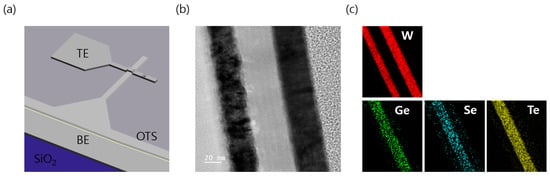
Figure 1.
(a) 3D structure of the W/GeSeTe/W, (b) Cross-sectional view of the W/GeSeTe(GST)/W, (c) Energy Dispersive X-ray Spectroscopy (EDS) of W/GeSeTe/W.
The ICP power was maintained at 300 W, while the substrate bias power was set to 20 W during the etching of the W layer. Ar and Cl2 gases at flow rates of 4 sccm (standard cubic centimeters per minute) and 30 sccm, respectively, were used in the dry-etching process. The temperature was controlled at 10 °C using a water-circulation cooling system to ensure optimal process conditions. The observed dry etching rate was approximately ~1.5 nm/s, indicating the effective removal of the material during the etching process. Subsequently, the W bottom electrode (BE) was washed with isopropyl alcohol and deionized water after removing the remaining photoresist (PR) with acetone. The GST layer was deposited using a sputtering device. The GeSeTe (35:50:15) and Te targets were deposited at a rate of 2 rpm through co-sputtering. A GeSeTe layer with a thickness of 50–60 nm was deposited via radiofrequency (RF) magnetron sputtering. The GeSeTe sputtered at 50 W and Te at 30 W power. The base pressure of the chamber was set to less than 4.0 × 10⁻⁶ Torr, and the working pressure was maintained at 2.0 × 10 Torr by maintaining the Ar (purity of 99.999%) flow. The upper W electrode was deposited with an OTS layer and then deposited and patterned using the lift-off method with a W target. A transmission electron microscope (TEM, JEOL, Akishima, Japan) analysis was conducted to analyze the detailed structure of the GeSeTe thin film. The samples used for TEM analysis were prepared using focused ion beam (FIB, crossbeam 540, Zeiss, Jena, Germany) techniques. Figure 1b presents a cross-sectional view of the W/GeSeTe(GST)/W structure, which highlights the layer arrangement and interfaces within the thin film. In addition, Figure 1c presents the results obtained through energy-dispersive X-ray spectroscopy (EDS, JEOL, Akishima, Japan), which depicts the elemental distribution of W, Ge, Se, and Te within the thin film. The EDS mapping clearly shows that each layer is precisely defined, indicating the accurate deposition and composition of the different materials.
3. Results
Figure 2a depicts the DC I-V curve, which is an electrical characteristic of the device. The Vth was within 1 V, and the on/off ratio was three orders of magnitude. Furthermore, the Ioff of the proposed OTS device was less than 10 nA. The compliance current (CC) was set to 100 μA, and (Keithley 4200) electrical pulse-based measurements were performed using a function generator (AFG, Agilent 81110A, Beaverton, OR, USA) oscilloscope (MSOX3024T, Tektronix, Beaverton, OR, USA), and the resistance state was confirmed. The resistance programming and verification were performed simultaneously owing to the volatile characteristics of the OTS device. The AFG, the tested OTS element, and the OSC were connected in series. Figure 2b depicts the measurement of the delay time when the OTS was turned on using the oscilloscope. It can be observed that the GeSeTe-based OTS device is converted in less than 10 ns; the device operates quickly when switching since it does not involve atomic rearrangement or structural changes [34,35].
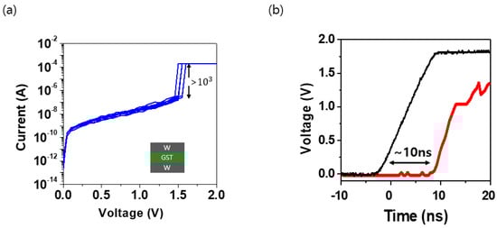
Figure 2.
(a) DC I–V curves of W/GeSeTe/W device, (b) turn–on voltage measured using an oscilloscope.
Figure 3a depicts the endurance performance of the OTS device. The volatile OTS is distinct from non-volatile memory such as resistive random-access memory (RRAM). A burst read scheme, which differs from the conventional approach of repeated write-and-read operations, was employed to evaluate its performance. After 10 to n numbers of pulses were applied to the OTS device cell the resistance of the OTS device was determined. This unique method enables a reduction in read damage when compared to conventional read schemes. We determined the resistance of the OTS cell by applying a specific number of pulses. This approach ensures accurate measurements while mitigating the potential for read-induced damage. Thus, the burst read scheme can be used to effectively assess the performance of an OTS device.
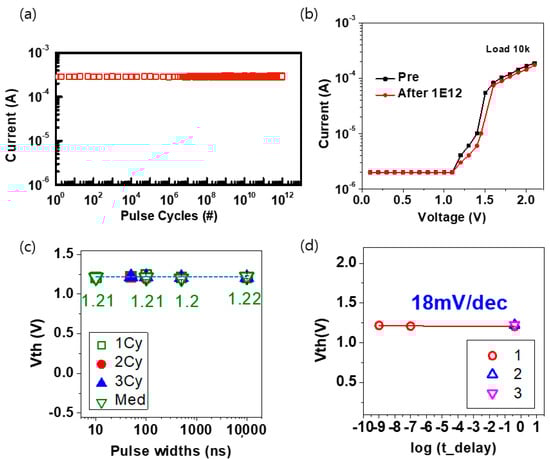
Figure 3.
(a) The endurance characteristics of the OTS device, (b) comparison of the pulse–based current-voltage (PIV) results before and after the endurance test, (c) threshold voltage (Vth) endurance with different pulse width, and (d) Vth shift with a delay time on a log scale.
Figure 3b presents a graph comparing the results of the pulse-based current-voltage (PIV) measurements before and after conducting 1 × 10¹² durability tests. This comparison verified the exceptional endurance performance of the OTS device, demonstrating its ability to maintain reliable performance over prolonged periods of usage.
Figure 3c depicts the change in the threshold voltage (Vth) between 10 ns and 10 μs pulse width. The results demonstrate minimal variation in the Vth value, indicating the consistent and stable operation of the OTS device regardless of the time. This demonstrates the fast and reliable switching capabilities of the OTS device while maintaining consistent performance over a time range of up to 10 s. Figure 3d presents the drift measurements of the OTS device. For the OTS based on chalcogenide materials, drift phenomena may occur over time, potentially affecting the overall device performance. The drift value must remain below 20 mV/dec to ensure successful commercialization. Figure 3d depicts the measured drift value of the GeSeTe volatile memory, which was 18 mV/dec. These results confirm the stability and reliability of the OTS device, further enhancing its practical applications and commercial potential.
In summary, the comprehensive analysis presented in Figure 3 highlights the exceptional endurance, fast and consistent operation, and ability to maintain stable performance over extended periods, owing to which the OTS device is a highly promising candidate for next-generation semiconductor technology.
Figure 4a,b presents a simple schematic diagram of a commercial transistor connected in series with and without the GeSeTe-based OTS device. The OTS was connected to the source part of the transistor, and the ground was held in the BE part for measurement. Figure 4c presents the transfer curve of a transistor without an OTS device, and Figure 4d presents the characteristics of a transistor with an OTS device connected in series. The commercial transistor used in this study was VN2222, which is an n-type MOSFET with a maximum voltage VDS of 60 V, maximum current ID of 0.26 A, and a maximum power PD of 0.3 W. In addition, the gate-source voltage (VGS) is ±20 V, gate voltage (VGS (th)) is 2–4 V, and the channel resistance (RDS (on)) is 18 Ω. The fixed drain voltages of Vth and 1V were applied during the IDS VGS sweep.
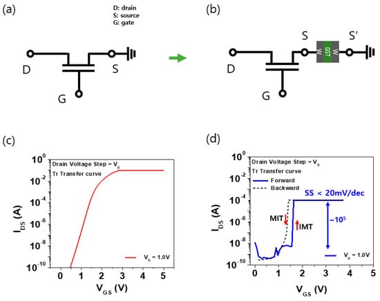
Figure 4.
(a) Schematics of transistors without the OTS device, (b) schematics of transistors with the device, and (c) IDS–VGS characteristics of a transistor without the GeSeTe–based OTS device, (d) with the device.
The power consumption of a transistor is divided into operating power consumption and standby power consumption. The operating voltage of the transistor and the standby current must be reduced simultaneously to achieve low power. Therefore, minimizing the SS value is crucial. The sub-threshold swing (SS) refers to the inverse of the transfer characteristics, the value obtained by taking semi-log of the (Id-Vg graph) drain current, divided by gate voltage. The sub-threshold swing (SS) is low in the sub-threshold voltage range because even a little reduction in voltage can easily control on/off, thereby reducing power consumption. The SS is low in the sub-threshold voltage range because even a little reduction in voltage can easily control on/off, thereby reducing power consumption. The SS value can be determined through Equation (1):
where Cd is the depletion layer capacitance and Cox is the gate oxide capacitance. At 300 K, the SS value is already 60 mV/dec, which can be determined by the equation. To reduce the SS value, we connected the OTS device to the transistor, and as a result, we were able to reduce the slope value. Comparing the SS values on the transmission curve shows that the SS values of the transistor-only devices (Figure 4b) are more than twice as different from those of the OTS devices (Figure 4c) connected in series. It succeeded in reducing the SS value to 20 mV/dec by connecting the transistor and the OTS element. A high on/off current ratio of more than 105 was also observed. When compared under the same conditions, the leakage current is also reduced.
Figure 5a depicts the obtained output characteristic curve, which is essential for understanding the operational characteristics of transistors, allowing the identification of the regions of transistor operation, where current amplification and voltage attenuation occurred. An analysis of the output curve demonstrated that the current compliance level varied with the step of the gate voltage. Figure 5b illustrates the case where the gate voltage is set to 1.5 V, controlling the current compliance at 100 μA. Since the pulse operation must be shown to measure the endurance, we checked the characteristics of the output curve after setting the transistor + OTS device to 1.5 V gate voltage. As a result, sweep operations were shown, followed by reliability measurements in hyper-FET. This enabled us to observe the output curve under specific conditions. The I-V curve depicted in Figure 5b demonstrates sweep behavior, followed by the measurement of reliability in the hyper-FET. This analysis of the output curves helps in obtaining an understanding of the operational regions and characteristics of the transistor, which further helps in appropriately designing transistors and establishing optimal operating conditions. Furthermore, for low-power logic devices such as the hyper-FET, the output curve analysis enables the evaluation of the tradeoff between power consumption and performance.
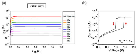
Figure 5.
(a) Output curve of transistor, (b) output curve of transistor + GeSeTe–based OTS device.
In the previous section, the endurance of the device was measured by adjusting the gate voltage step in accordance with the output power curve. An endurance test was conducted, and the results are presented in Figure 6a. The measurement results confirmed that the device could withstand up to 108 pulses without significant degradation, and the pulse width was measured to be 50 ns.
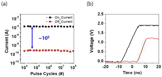
Figure 6.
(a) AC endurance up to 108 cycles (b) delay–time during pulse application.
Subsequently, the pulse waveform was analyzed when the switching characteristics were verified by bonding the transistor and the GeSeTe-based OTS device in series, as shown in Figure 6b. It was determined that the gate delay operated within 20 ns, demonstrating the effectiveness of the device in switching applications. Overall, these findings provide valuable insights into the performance and reliability of the device, which may be useful for designing and optimizing similar devices in the future.
4. Conclusions
Research on ultralow-voltage beyond-CMOS technology, which can significantly reduce the leakage power and driving voltage, is becoming increasingly important for the development of next-generation semiconductor technologies. The SS of the existing MOSFETs cannot be reduced below 60 mV/dec at room temperature owing to the thermionic carrier injection mechanism in the source region.
This study presented a GeSeTe-based OTS device with the advantages of a fast-switching speed and low leakage current to overcome the SS limit of MOSFETs at room temperature. These OTS devices were connected in series with transistors to analyze the changes in the SS. The proposed GeSeTe-based OTS device exhibited excellent characteristics including a leakage current of less than 10 nA, steep on/off slope of over 103, and fast switching speed. Additionally, these devices demonstrated high endurance and operated stably for up to 1012 cycles.
Consequently, the hyper-FET formed by connecting the OTS device with transistors presented an improved performance when compared with standalone transistors and confirmed stable endurance for up to 108 cycles. The OTS device connected in series with the transistors presented an SS of less than 20 mV/dec and a high ION/IOFF ratio of over 105. We have identified the potential to overcome the physical limitations of SS at 60 mV/dec and improve both performance and energy efficiency. The development of SS in FET technology is expected to have a significant impact on the energy-efficient modern society. This result not only improves the performance of the MOSFET but also. As more and more applications are required to implement features such as IoT and wearable processors at ultra-low power, these technologies can be used effectively in circuit systems that require ultra-low power. This will help improve technology and price competitiveness. It can also reduce the power consumption of existing electronic components that are high in power consumption, improving operational life. It is expected to contribute to the development of semiconductor technology in the future and promote energy conservation and the development of high-performance electronic devices.
Author Contributions
Experiments and writing, S.Y.L.; conceptualization, H.K.S., S.Y.J. and M.K.Y.; supervision, M.K.Y. All authors have read and agreed to the published version of the manuscript.
Funding
This study was supported by the Sahmyook University Research Fund in 2021.
Institutional Review Board Statement
Not applicable.
Informed Consent Statement
Not applicable.
Data Availability Statement
Not applicable.
Conflicts of Interest
The authors declare no conflict of interest.
References
- Koswatta, S.O.; Koester, S.J.; Haensch, W. On the possibility of obtaining MOSFET-like performance and sub-60-mV/dec swing in 1-D broken-gap tunnel transistors. IEEE Trans. Electron Devices 2010, 57, 3222–3230. [Google Scholar] [CrossRef]
- Choi, W.Y.; Park, B.-G.; Lee, J.D.; Liu, T.-J.K. Tunneling field-effect transistors (TFETs) with subthreshold swing (SS) less than 60 mV/dec. IEEE Electron Device Lett. 2007, 28, 743–745. [Google Scholar] [CrossRef]
- Wang, S.; Wang, J.; Zhi, T.; Xue, J.; Chen, D.; Wang, L.; Zhang, R. Cold source field-effect transistors: Breaking the 60-mV/decade switching limit at room temperature. Phys. Rep. 2023, 1013, 1–33. [Google Scholar] [CrossRef]
- Haensch, W.; Nowak, E.J.; Dennard, R.H.; Solomon, P.; Bryant, A.; Dokumaci, O.; Kumar, A.; Wang, X.; Johnson, J.; Fischetti, M. Silicon CMOS devices beyond scaling. IBM J. Res. Dev. 2006, 50, 339–361. [Google Scholar] [CrossRef]
- Frank, D.J.; Dennard, R.H.; Dennard, E.; Solomon, P.M.; Taur, Y.; Wong, H.-S.P. Device scaling limits of Si MOSFETs and their application dependencies. Proc. IEEE 2001, 89, 259–288. [Google Scholar] [CrossRef]
- Jung, H.; Chang, J.; Yoo, C.; OH, J.; Choi, S.; Wong, J. Hyper-FET’s Phase-Transition-Materials Design Guidelines for Ultra-Low Power Applications at 3 nm Technology Node. Nanomaterials 2022, 12, 4096. [Google Scholar] [CrossRef]
- Yan, S.-C.; Sun, C.-H.; Sun, C.J.; Lin, Y.-W.; Yao, Y.-J.; Wu, Y.-C. Trench FinFET Nanostructure with Advanced Ferroelectric Nanomaterial HfZrO2 for Sub-60-mV/Decade Subthreshold Slope for Low Power Application. Nanomaterials 2022, 12, 2165. [Google Scholar] [CrossRef] [PubMed]
- Meindl, J.D.; Chen, Q.; Davis, J.A. Limits on Silicon Nanoelectronics for Terascale Integration. Science 2001, 193, 2044–2049. [Google Scholar] [CrossRef]
- Kobayashi, M. A perspective on steep-subthreshold-slope negative-capacitance field-effect transistor. Appl. Phys. Express 2018, 11, 110101. [Google Scholar] [CrossRef]
- Nirschl, T.; Henzler, S.; Fischer, J.; Fukle, M.; Bargagli-Stoffi, A.; Sterkel, M.; Sedlmeir, J.; Weber, C.; Heinrich, R.; Schaper, U.; et al. Scaling properties of the tunneling field effect transistor (TFET): Device and circuit. Solid-State Electron. 2006, 50, 44–51. [Google Scholar] [CrossRef]
- Bhuwalka, M.K.; Schindler, M.; Abelein, U.; Schmidt, M.; Sulima, T.; Eisele, I. Tunnel FET: A CMOS device for high temperature applications. In Proceedings of the 25th International Conference on Microelectronics, Belgrade, Serbia, 14–17 May 2006; pp. 124–127. [Google Scholar]
- Guo, S.; Prentki, R.J.; Jin, K.; Chen, C.-L.; Guo, H. Negative-Capacitance FET With a Cold Source. IEEE Trans. Electron Devices 2021, 68, 911–918. [Google Scholar] [CrossRef]
- Appenzeller, J.; Lin, Y.M.; Knoch, J.; Avouris, P. Band-to-band Tunneling in Carbon Nanotube Field-Effect Transistors. Phys. Rev. Lett. 2004, 93, 196805. [Google Scholar] [CrossRef] [PubMed]
- Ionescu, A.M.; Riel, H. Tunnel Field-Effect Transistors as Energy-Efficient Electronic Switches. Nature 2011, 479, 329–337. [Google Scholar] [CrossRef] [PubMed]
- Shin, G.H.; Koo, B.; Park, H.; Woo, Y.; Lee, J.E.; Choi, S.Y. Vertical-Tunnel Field-Effect Transistor Based on a Silicon-MoS2 Three-Dimensional-Two-Dimensional Heterostructure. ACS Appl. Mater. Interfaces 2018, 10, 40212–40218. [Google Scholar] [CrossRef]
- Cao, W.; Sarkar, D.; Khatami, Y.; Kang, J.; Banerjee, K. Subthreshold-Swing Physics of Tunnel Field-Effect Transistors. AIP Adv. 2014, 4, 067141. [Google Scholar] [CrossRef]
- Jo, J.; Shin, C. Negative Capacitance Field Effect Transistor With Hysteresis-Free Sub-60-mV/Decade Switching. IEEE Electron Device Lett. 2016, 37, 245–248. [Google Scholar] [CrossRef]
- Morin, F.J. Oxides Which Show a Metal-to-Insulator Transition at the Neel Temperature. Phys. Rev. Lett. 1959, 3, 34–36. [Google Scholar] [CrossRef]
- Berglund, C.N.; Guggenheim, H.J. Electronic Properties of VO2 near the Semiconductor-Metal Transition. Phys. Rev. 1969, 185, 1022–1033. [Google Scholar] [CrossRef]
- Yi, W.; Tsang, K.K.; Lam, S.K.; Bai, X.; Crowell, J.A.; Flores, E.A. Biological plausibility and stochasticity in scalable VO2 active memristor neurons. Nat. Commun. 2018, 9, 4661. [Google Scholar] [CrossRef] [PubMed]
- Morrison, V.R.; Chatelain, R.P.; Tiwari, K.L.; Hendaoui, A.; Bruhács, A.; Chaker, M.; Siwick, B.J. A photoinduced metal-like phase of monoclinic VO2 revealed by ultrafast electron diffraction. Science 2014, 346, 445–448. [Google Scholar] [CrossRef]
- Kim, H.T.; Lee, Y.W.; Kim, B.J.; Chae, B.G.; Yun, S.J.; Kang, K.Y.; Han, K.J.; Yee, K.J.; Lim, Y.S. Monoclinic and correlated metal phase in VO2 as evidence of the Mott transition: Coherent phonon analysis. Phys. Rev. Lett. 2006, 97, 266401. [Google Scholar] [CrossRef]
- Tao, Z.; Zhou, F.; Han, T.T.; Torres, D.; Wang, T.; Sepulveda, N.; Chang, K.; Young, M.; Lunt, R.R.; Ruan, C.Y. The nature of photoinduced phase transition and metastable states in vanadium dioxide. Sci. Rep. 2016, 6, 38514. [Google Scholar] [CrossRef]
- Zhang, S.; Chou, J.Y.; Lauhon, L.J. Direct Correlation of Structural Domain Formation with the Metal Insulator Transition in a VO2 Nanobeam. Nano Lett. 2009, 9, 4527–4532. [Google Scholar] [CrossRef] [PubMed]
- Qazilbash, M.M.; Brehm, M.; Chae, B.-G.; Ho, P.-C.; Andreev, G.O.; Kim, B.-J.; Yun, S.J.; Balatsky, A.V.; Maple, M.B.; Keilmann, F.; et al. Mott Transition in VO2 Revealed by Infrared Spectroscopy and Nano-Imaging. Science 2007, 318, 1750–1753. [Google Scholar] [CrossRef] [PubMed]
- Redaelli, A.; Pirovano, A.; Benvenuti, A.; Lacaita, A. Steep Slope Field-Effect Transistors with Ag/TiO2-Based Threshold Switching Device. IEEE Electron Device Lett. 2016, 37, 16105152. [Google Scholar]
- Song, J.; Woo, J.; Prakash, A.; Lee, D.; Hwang, H. Threshold selector with high selectivity and steep slope for cross-point memory array. IEEE Electron Device Lett. 2015, 36, 681. [Google Scholar] [CrossRef]
- Wang, Z.; Rao, M.; Midya, R.; Joshi, S.; Jiang, H.; Lin, P.; Song, W.; Asapu, S.; Zhuo, Y.; Li, C.; et al. Threshold Switching of Ag or Cu in Dielectrics: Materials, Mechanism, and Applications. Adv. Funct. Mater. 2018, 28, 1704862. [Google Scholar] [CrossRef]
- Velea, A.; Opsomer, K.; Devulder, W.; Dumortier, J.; Fan, J.; Detavernier, C.; Jurczak, M.; Govoreanu, B. Te-based chalcogenide materials for selector applications. Sci. Rep. 2017, 7, 8103. [Google Scholar] [CrossRef]
- Zhu, M.; Ren, K.; Song, Z. Ovonic threshold switching selectors for three-dimensional stackable phase-change memory. MRS Bull. 2019, 44, 715. [Google Scholar] [CrossRef]
- Seo, H.K.; Ryu, J.J.; Lee, S.Y.; Park, M.; Park, S.G.; Song, W.; Kim, G.H.; Yang, M.K. Material and structural engineering of ovonic threshold switch for highly reliably performance. Adv. Electron. Mater. 2022, 8, 2200161. [Google Scholar] [CrossRef]
- Seong, D.; Lee, S.Y.; Seo, H.K.; Kim, J.-W.; Park, M.; Yang, M.K. Highly Reliable Ovonic Threshold Switch with TiN/GeTe/TiN Structure. Materials 2023, 16, 2066. [Google Scholar] [CrossRef]
- Redaelli, A.; Pirovano, A.; Benvenuti, A.; Lacaita, A. Threshold switching and phase transition numerical models for phase change memory simulations. J. Appl. Phys. 2008, 103, 111101. [Google Scholar] [CrossRef]
- Adler, D.; Shur, M.S.; Silver, M.; Ovshinsky, S.R. Threshold switching in chalcogenide-glass thin films. J. Appl. Phys. 1980, 51, 3289. [Google Scholar] [CrossRef]
- Chen, Z.; Tong, H.; Li, X.; Wang, L.; Zhao, R.; Gu, W.; Miao, Z. Experimental evidence for non-purely electric field-induced threshold switching and modified thermal-assisted model in GeTe phase change material. Appl. Phys. Lett. 2021, 118, 203502. [Google Scholar] [CrossRef]
- Clima, S.; Garbin, D.; Devulder, W.; Keukelier, J.; Opsomer, K.; Goux, L.; Kar, G.S.; Pourtois, G. Material relaxation in chalcogenide OTS SELECTOR materials. Microelectron. Eng. 2019, 215, 110996. [Google Scholar] [CrossRef]
- Clima, S.; Ravsher, T.; Garbin, D.; Degraeve, R.; Fantini, A.; Delhougne, T.; Kar, G.S.; Pourtois, G. Ovonic Threshold Switch Chalcogenides: Connecting the First-Principles Electronic Structure to Selector Device Parameters. ACS Appl. Electron. Mater. 2023, 5, 461–469. [Google Scholar] [CrossRef]
- Woo, J.; Lee, D.; Park, J.; Song, J.; Hwang, H. Steep Slope Field-Effect Transistors With B-Te-Based Ovonic Threshold Switch Device. ACS Nano 2012, 6, 8166. [Google Scholar]
- Wang, X.; Li, H. A steep-slope tellurium transistor with a native voltage amplifying threshold switch. Appl. Phys. Lett. 2022, 120, 223502. [Google Scholar] [CrossRef]
- Kang, C.; Choi, H.; Son, H.; Kang, T.; Lee, S.-M.; Lee, S. A steep-switching impact ionization-based threshold switching field-effect transistor. Nanoscale 2023, 15, 5771–5777. [Google Scholar] [CrossRef]
Disclaimer/Publisher’s Note: The statements, opinions and data contained in all publications are solely those of the individual author(s) and contributor(s) and not of MDPI and/or the editor(s). MDPI and/or the editor(s) disclaim responsibility for any injury to people or property resulting from any ideas, methods, instructions or products referred to in the content. |
© 2023 by the authors. Licensee MDPI, Basel, Switzerland. This article is an open access article distributed under the terms and conditions of the Creative Commons Attribution (CC BY) license (https://creativecommons.org/licenses/by/4.0/).