Article

The Optical and Thermo-Optical Properties of Non-Stoichiometric Silicon Nitride Layers Obtained by the PECVD Method with Varying Levels of Nitrogen Content

by
Stanisława Kluska
1,
Maria Jurzecka-Szymacha
1,*,
Natalia Nosidlak
2,
Piotr Dulian
3 and
Janusz Jaglarz
4,*
1
Faculty of Materials Science and Ceramics, AGH University of Science and Technology, Mickiewicza Avenue 30, 30-059 Krakow, Poland
2
Department of Physics, Cracow University of Technology, Podchorążych Street 1, 30-084 Krakow, Poland
3
Faculty of Chemical Engineering and Technology, Cracow University of Technology, Warszawska Street 24, 31-155 Krakow, Poland
4
Institute of Materials Engineering, Cracow University of Technology, Jana Pawła II Avenue 37, 31-864 Krakow, Poland
*
Authors to whom correspondence should be addressed.
Materials 2022, 15(6), 2260; https://doi.org/10.3390/ma15062260
Submission received: 16 February 2022 / Revised: 11 March 2022 / Accepted: 16 March 2022 / Published: 18 March 2022

Abstract

:
In this paper, we investigated the optical and thermo-optical properties of a-SiNx:H layers obtained using the PECVD technique. SiNx:H layers with different refractive indices were obtained from silane and ammonia as precursor gases. Surface morphology and chemical composition studies were investigated using atomic force microscopy, scanning electron microscopy, Fourier transform infrared spectroscopy and energy dispersive spectrometry methods. Spectroscopic ellipsometry was used to determine the optical indexes, thicknesses and optical bandgap of the films. The main purpose was to identify the thermo-optical characteristics of layers with different refractive indexes. Thermo-optical studies were performed to determine the temperature hysteresis of optical parameters. These measurements showed that after annealing up to 300 °C and subsequent cooling, the value of optical parameters returned to the initial values.

1. Introduction

Amorphous SiNx:H layers have been known since the eighties and are still used for various optical applications. They are mainly used as very effective antireflection coatings in the production of crystalline silicon (c-Si) and multicrystalline silicon (mc-Si) solar cells [1,2]. The hydrogen content in the layers effectively passivates the material’s surface and suppresser surface recombination [3,4,5,6,7,8]. SiNx:H layers with various levels of nitrogen content are widely used in optoelectronics. Their main applications are as gate dielectrics in thin film transistors, in photonics, phototransistors and image sensors, or as multilayer systems for antireflection coatings in the infrared range [9,10,11,12]. The plasma-enhanced chemical vapour deposition (PECVD) technique is currently one of the most preferred deposition methods for the a-SiNx:H layers. This is due to the lower energy consumption during the process and the high hydrogen content in the layer [13,14,15]. These layers can also be obtained by other CVD techniques, such as atomic layer deposition (ALD) and catalytic (Cat-CVD), and other layer techniques, such as magnetron sputtering and ion-implantation [16,17,18,19]. It is known that the properties of a-SiNx:H layers, such as the extinction coefficient and the optical band gap, can be adjusted by varying the composition ratio of Si and N or by changing the deposition temperature [20,21]. There has been a lot of research on the effect of the processing parameters (Si/N ratios and Si-H/N-H bond ratios in layers deposited) on the optical parameters of silicon nitride films grown from a SiH4, NH3 and N2 mixture [22,23]. The authors present the relationship between the Si/N ratio and refractive index [24]. It is known that, as the nitrogen content of the layer decreases, the refractive index value increases [25].
In this paper, we report unpublished results of the optical and thermo-optical properties of the hydrogenated amorphous silicon nitride layers—specifically conventional silicon nitride (SiNx) and silicon-rich silicon nitride (Si-rich SiNx) deposited on Si(001) and on glass (fused quartz). We present their optical and thermo-optical analyses before and after a heating process to temperatures up to 300 °C. The layers were deposited using a wide gaseous flow range [SiH4]/[NH3], thus receiving a wide range of the Si/N ratio in the layers. The calculated thermo-optic coefficient (TOC) was used for the thermal characterisation of optical properties. Thermo-optical studies have indicated that heating and cooling cycles are repeatable; the values of n and k almost coincide with the values after heating/cooling processes. In the literature, thermos-optical results for SiN:H layers containing different contents of nitrogen have been presented, but not in the wide range we present. Our study allowed us to find a nonlinear dependence of the refractive index on the nitrogen content of the film.

2. Materials and Methods

2.1. Technology and Samples

For the purpose of this work, two series of samples were fabricated using the PECVD technique. All the layers were deposited on crystalline silicon (001)—oriented from gaseous silane and ammonia, and fused quartz (samples 6–8). Before deposition, the substrates were cleaned: samples 1–5 were preliminary washed in acetone and isopropyl alcohol and then placed in the reactor; for samples 6–8, organic matter was first removed from the wafer surfaces using ultrasonic cleaning in an acetone solution for 20 min then immersion in 5% HF acid to remove the native oxide layer before being transported into the deposition chamber.
The deposition was performed by the PECVD method using the Plasmalab System 100 from Oxford Plasma Technology and the multi-module MW-RFCVD Elettrorava system. The excitation frequencies were a low frequency, (LF) 90–450 kHz, and a high frequency (HF), 13.56 MHz. The layers were obtained at 220 °C and 310 °C from silane and ammonia, used as the gas mixture. The chamber pressure was kept constant (53 Pa) during the obtained process. Layers 6 and 7 were obtained at HF and LF frequencies alternately during one deposition, and other layers only at the HF frequency. Directly before layer deposition, the substrates were etched for 10 min of cleaning in an argon plasma environment. The other process parameters are presented in Table 1.

2.2. Characterization Methods

The measurements of the chemical composition and surface morphology for the obtained layers were performed on a scanning electron microscope (NOVA NANOSEM 200, FEI EUROPE Company, (Oregon, OR, USA) and an energy dispersive spectrometer (EDAX Genesis, Paoli, PA, USA). The chemical composition and Si/N ratio in the layer were evaluated by the EDX technique (Genesis, Paoli, PA USA). Obtained films were also characterised by X-ray diffraction (XRD, X’Pert Philips, Almelo, Netherlands) using the Philips X’Pert diffractometer with a CuKα radiation source (λ = 1.54056 Å) for 2θ = 6–90° with a step size of 0.01°. The layers were analysed with FTIR (Brucker, Billerica, MA, USA) and spectroscopic ellipsometry (SE, manufacturer.A.Woollam, Lincoln, NE, USA). Subsequently, the Fourier transform infrared (FTIR) spectrum of layers was measured within the range of 400–4000 cm−1 using the Vertex Brucker 70 V (Brucker, Billerica, MA, USA) (resolution 4 cm−1, 275 scans). Atomic force microscopy (AFM, XE-70 Park System Corp., Suwon, Korea) imaging was performed using a CoreAFM scanning-probe microscope (Nanosurf AG, Liestal, Switzerland) operating in a contact-force mode. A 256 × 256 pixel resolution was used for all AFM topography images.
The thermo-optic properties of SiN layers have been examined using the spectroscopic ellipsometry (SE) technique. SE measurements were performed with the use of a Woollam M-2000 ellipsometer (Woollam Co. Inc., Lincoln, NE, USA) with a spectral range of 193 to 1690 nm. The M-2000 ellipsometer was additionally equipped with a heat cell to change the sample temperature. Samples were heated from room temperature up to 300 °C in an air atmosphere under normal pressure conditions.
SE is a nondestructive and noncontact method that enables measuring such optical properties of thin films as optical constants, thickness and energy bandgap. The changes in a polarisation state have been registered as ellipsometric Ψ and Δ spectra for an incident angle of 70°. Ellipsometric parameter Ψ represents the amplitude ratio and the Δ parameter represents the phase difference between p and s polarised light waves. Both parameters Ψ and Δ are related and fulfil the fundamental equation of ellipsometry (Equation (1)) [26,27]:
p   =   tan Ψ · e i Δ
In order to determine dispersion relations of optical indices, namely refractive index n(E) and extinction coefficient k(E), the Tauc–Lorentz (TL) parameterisation model [28,29] has been applied. The Tauc–Lorentz model is Kramers–Krönig (K–K) which is consistent and physically correct; therefore, it is successfully employed for amorphous semiconductors and dielectrics [30,31,32]. The imaginary part of the dielectric function ε2 in the TL model is a result of the multiplication of the Lorentz oscillator function εL(E) (Equation (2)) and the Tauc function εT(E) (Equation (3)):
ε L E   =   A L · E g · Γ · E E 2 E 0 2 2 + Γ 2 E 2
ε T E   >   E g   =   A T E E g E 2
where AL is the strength of the imaginary part of the ε2 dielectric function, Γ is the broadening of the peak and E0 is the central energy of the peak, AT is the Tauc coefficient, E is the photon energy and Eg is the optical bandgap. The εT(E) function is equal to zero below the bandgap.
In order to obtain the best agreement between the model and the measurement data, the Gauss model was additionally used in optical modelling. The Gauss oscillators are often used with the Tauc–Lorentz model as multiplicative factors. The imaginary part of the dielectric function of the Gauss model εG(E) is given in Equation (4) [33]:
ε G ( E )   =   A G exp E E 0 σ 2 + exp E + E 0 σ 2
where σ   =   Γ / 2 l n 2 and AG is the amplitude.
The imaginary and real part of the dielectric function are linked by the K–K relations. Therefore, the real part of the dielectric function of the Tauc–Lorentz and Gauss model can be calculated based on K–K consistency.
Thermo-optical properties of transparent films have been described using the Prod’homme theory [34]. The most important parameters describing optical and physical properties are the thermo-optical coefficient (TOC) and the thermal expansion coefficient (TEC). The TOC is defined as a derivative of the refractive index relative to temperature TOC = dn/dT, while TEC is defined as the thickness derivative over temperature TEC = d ( t h i c k n e s s ) d T .

3. Results

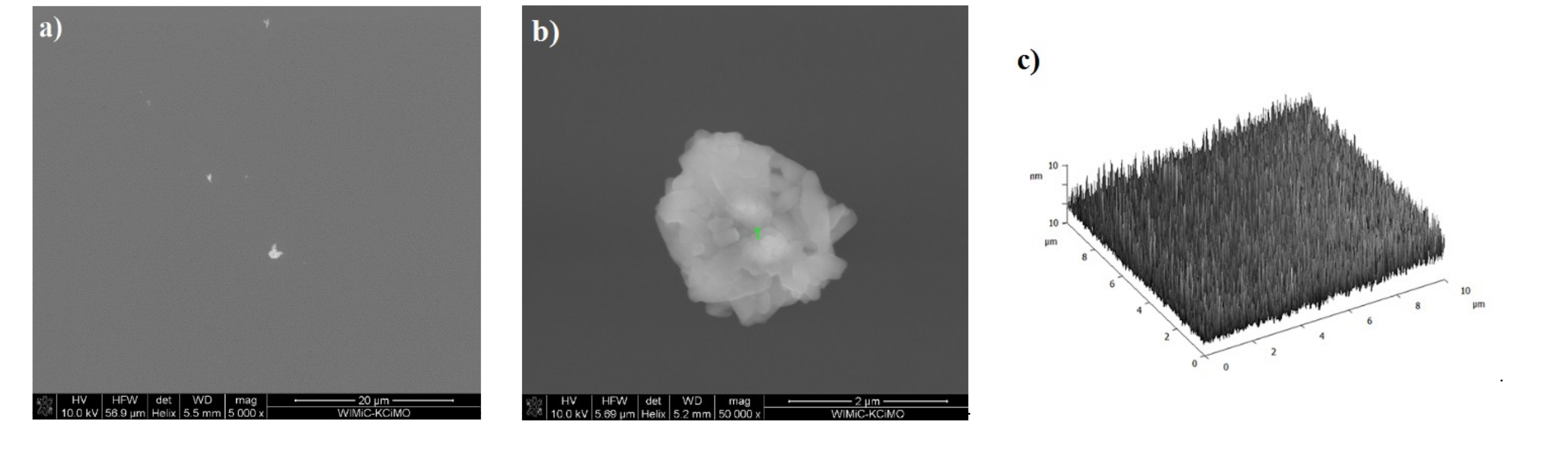
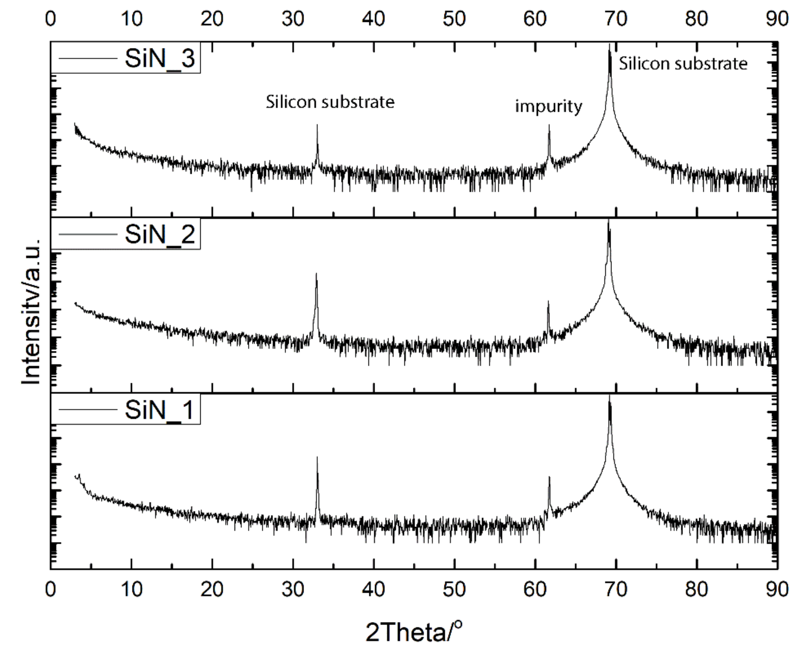
3.1. Morphology and Chemical Structure of Layers

SEM and AFM morphology studies performed of all SiN samples confirmed the high quality of the produced amorphous layers (shown in Figure A1 in Appendix A section). All samples were very similar in terms of surface morphology. The surface exhibits high homogeneity without any large-scale defects, cracks. It is smooth and uniform. Only in a small area, few impurities are visible (Figure A1a and Figure A2 in Appendix A section). The surface roughness (RMS value), determined on the basis of AFM tests for all tested samples, was very similar to each other and was approximately 7 nm.
The chemical composition of the layers was roughly estimated by the EDS technique (Genesis, Paoli, PA, USA) and the value of the Si/N ratio is presented in Table 2. The amorphous of the SiN layers was confirmed by X-ray diffraction measurements (X’Pert Philips, Almelo, The Netherlands). In all tested samples, there were diffraction reflections corresponding to Si (001) substrate and a small amount of impurities (see Appendix A section Figure A3).
The structural characterisation of the a-SiN:H layers were performed by means of FTIR spectroscopy in the absorption mode, and in the range of 400 to 4000 cm−1.The FTIR absorption spectra are typical for a-SiN:H layers containing the peaks of chemical bonds Si–N, N–H, Si–H and were presented in papers [11,35]. The assignments of the infrared vibration modes of the a-SiN:H layer are reported in Table 3.
It was observed that with the increase of the gas-flow ratio, the intensity of bond peaks of Si–N (820–890 cm−1), Si–H, and N–H (at 1139 cm−1) increases, and the intensity of the bond peaks of N–H (at 3343 cm−1) decreases. With the increased s ratio, more connections with nitrogen are created (N–H bending at 1139 cm−1). In the case of the N–H stretching bond (at about 3343 cm−1), its density decreased with s.

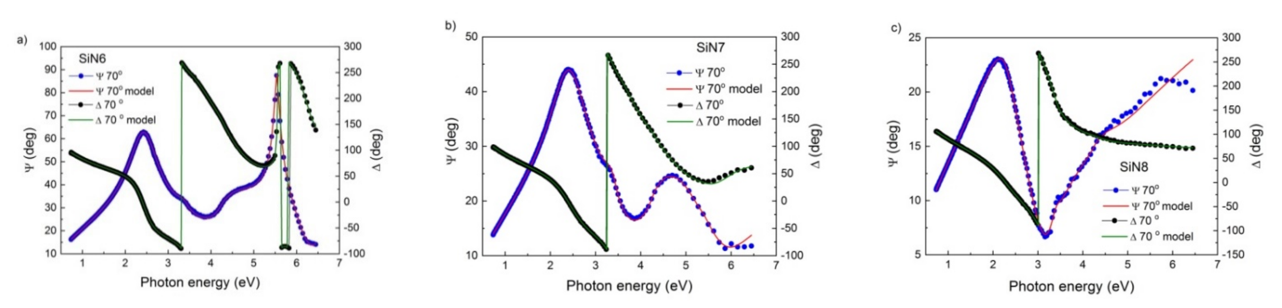
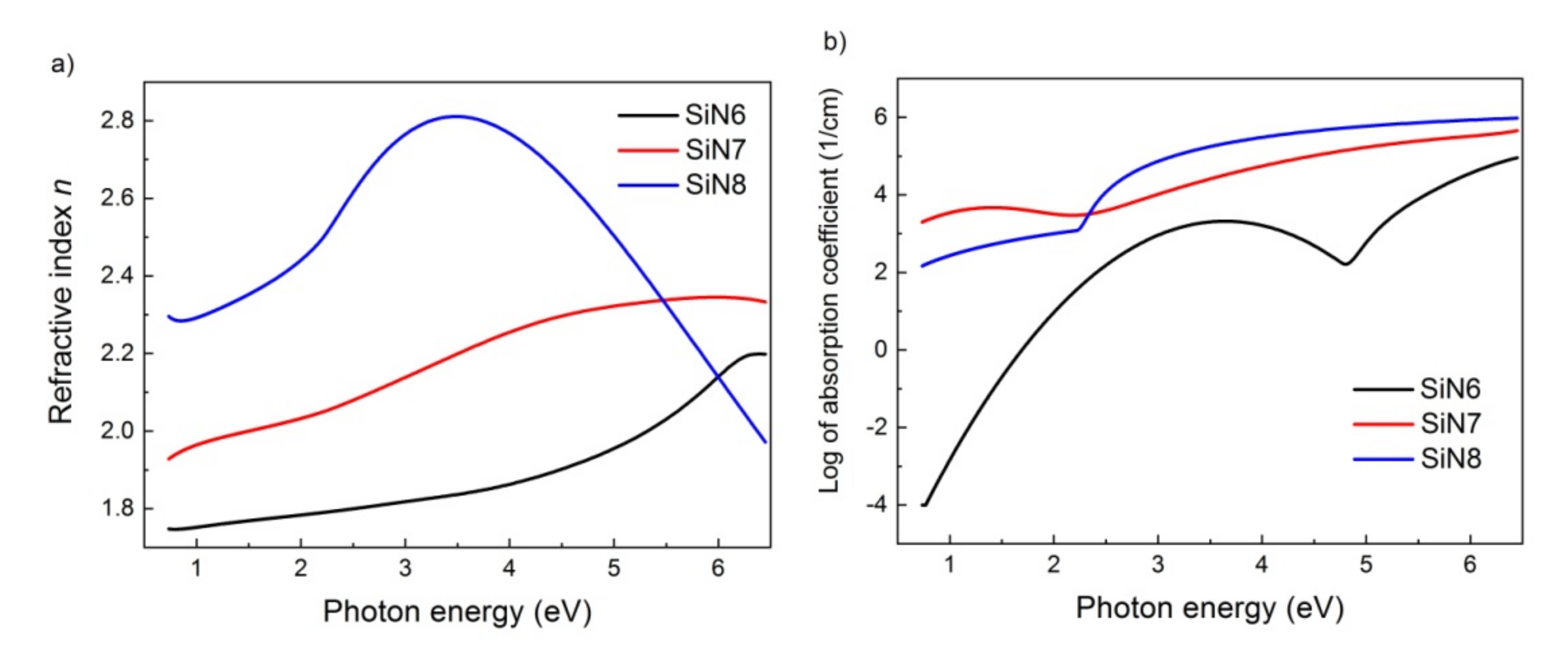
3.2. Optical Studies

All ellipsometric studies were performed for three samples on silicon SiN6, SiN7, and SiN8 for a 70° angle of incidence across the full spectral range (193 to 1690 nm or 0.7 to 6.5 eV). The same three SiN layers have been applied on fused silica, which enabled us to measure transmission spectra. The data were analysed using CompleteEASE 5.15 software. Spectral dependences of Ψ and Δ for three samples are presented in Figure 1a–c. The mean squared error (MSE) values determined using the Levenberg–Marquardt method are presented in Table 4. The Tauc–Lorentz model was used to approximate the experimental results. The value of MSE confirms the fact that experimental data are in good agreement with the applied TL model. Small discrepancies between the measurement data and the applied model are visible in the UV region. The following parameters from the TL model at various wavelengths are summarised in Table 4: bandgap Eg, amplitude A, broadening B, and refractive index values. The Eg values strongly depend on the layer preparation process conditions. The determined values of Eg have been confirmed in other works [38,39].
On the basis of the applied model, the dispersion relations of the refractive index n(E) and extinction coefficient k(E) for three SiN layers on silicon are shown in Figure 2. As can be observed, hydrogenated amorphous silicon-rich nitride exhibits high transparency in the photon energy range of 0.7 to 2.2 eV, i.e., in the visible and near-infrared spectrum area.
Figure 3 shows the refractive index n value at 632 nm as a function of the Si/N ratio for the samples presented in Table 2. As can be seen, a strong dependence of refractive index versus Si/N ratio (above 7) occurs. For the low Si/N ratio, it is difficult to determine the relationship between the refractive index versus Si/N.
In Figure 4, the influence of temperature on the thickness of SiN layers (SiN6, SiN7, and SiN8) in the heating and cooling cycle is shown. The difference of thickness before and after temperature treatment is about 2 nm, which means that all SiN layers are thermally stable. For the temperature range of 25 to 300 °C, the TEC values were determined at 400 nm and are presented in Table 5.
The thermal hysteresis of refractive index n for various wavelengths (400, 632, 900, and 1500 nm) is presented in Figure 5. The changes of n with the temperature are linear, i.e., there is no form of a hysteresis loop. Refractive index values at 25 °C before and after temperature treatment are nearly identical. This enabled us to draw the conclusion that this thermodynamical process is reversible. Thus, the tested layers can be successfully applied in optics. The exception is n(T) at 1500 nm for SiN6, where the difference between the initial and final values of n is about 0.01. For the temperature range of 25 to 300 °C, the TOC values were determined at various wavelengths and are presented in Table 5.
The refractive index of the amorphous layers is a linear function of temperature and can take positive and negative values. The slope dn/dT (TOC) is given by differentiating the Lorentz–Lorenz equation, which is a function of the refractive index, polarisation coefficient Φ and volumetric expansion coefficient β, which is given by express as Equation (5):
d n / d T   =   n 2 1 n 2 + 2 6 n   ·   Φ β
If β > Φ then TOC becomes negative. As can be seen from the formula, the slope may change as a result of the refractive index n dispersion. Therefore, the slopes dn/dT for different wavelengths may change (for zero dispersion, the slopes should be the same). Figure 6 shows the thermal dependences of extinction coefficient k(T) at 400 nm. The linear dependence of the extinction coefficient k versus temperature appears for energy above the absorption band (2.4 eV). For the SiN8 sample, the extinction coefficient slightly changes with temperature, but the changes of k for SiN6 and SiN7 samples are negligible. Sample SiN8 exhibits a higher extinction than other tested samples. Such high k values affect the positive sign of the TOC coefficient in the absorption area.
The optical parameters of the tested layers are presented in Table 4 and TOC, TEC and thickness values are presented in Table 5. The TOC depends mainly on the polarizability of the layer and on the value of the TEC. If the TEC value is high, the TOC takes a negative value. The TOC values determined for 400 nm and 500 nm wavelengths are positive for the SiN8 sample. This is due to the absorption in the SiN8 sample, for which the temperature dependence is shown in Figure 7. The TEC values presented in Table 5 are high compared to relating to other materials [40,41,42].
We observed that the TOC values for the SiN6, SiN7 and SiN8 samples depend on the wavelength, while the TOC values for the SiN layers, presented in other works [35,43], do not show such a relationship. The slope of the n(T) dependence is nearly the same for all wavelengths in the transparency region. In this work, we observed a strong dependence of TOC values versus wavelength. Additionally, the inclination angle of linear dependence n(T) for a particular sample decreases with the wavelength, and thus the TOC value decreases. For samples presented in the literature [35,43], the value of the refractive index n increased with temperature. For SiN layers presented in this work, the n values decreased with increasing temperature.
These results are a consequence of the much higher gas-flow ratios for samples 2–5 deposited at only HF frequency. The second reason is the different synthesis methods used in samples preparations. Two frequencies, LF and HF, were used in the process of producing the SiN6, SiN7, and SiN8 samples.
The transmission spectra presented in Figure 8 were measured for the layers applied on the fused silica and were included during the fitting of the TL model to the ellipsometric results.

4. Conclusions

This paper presents the optical and thermo-optical dependences for non-stoichiometric silicon nitride layers obtained by two independent PECVD methods with varying levels of nitrogen content. The presented SiN layers were fully amorphous, without large-scale defects and cracks. The ellipsometric investigations showed that:
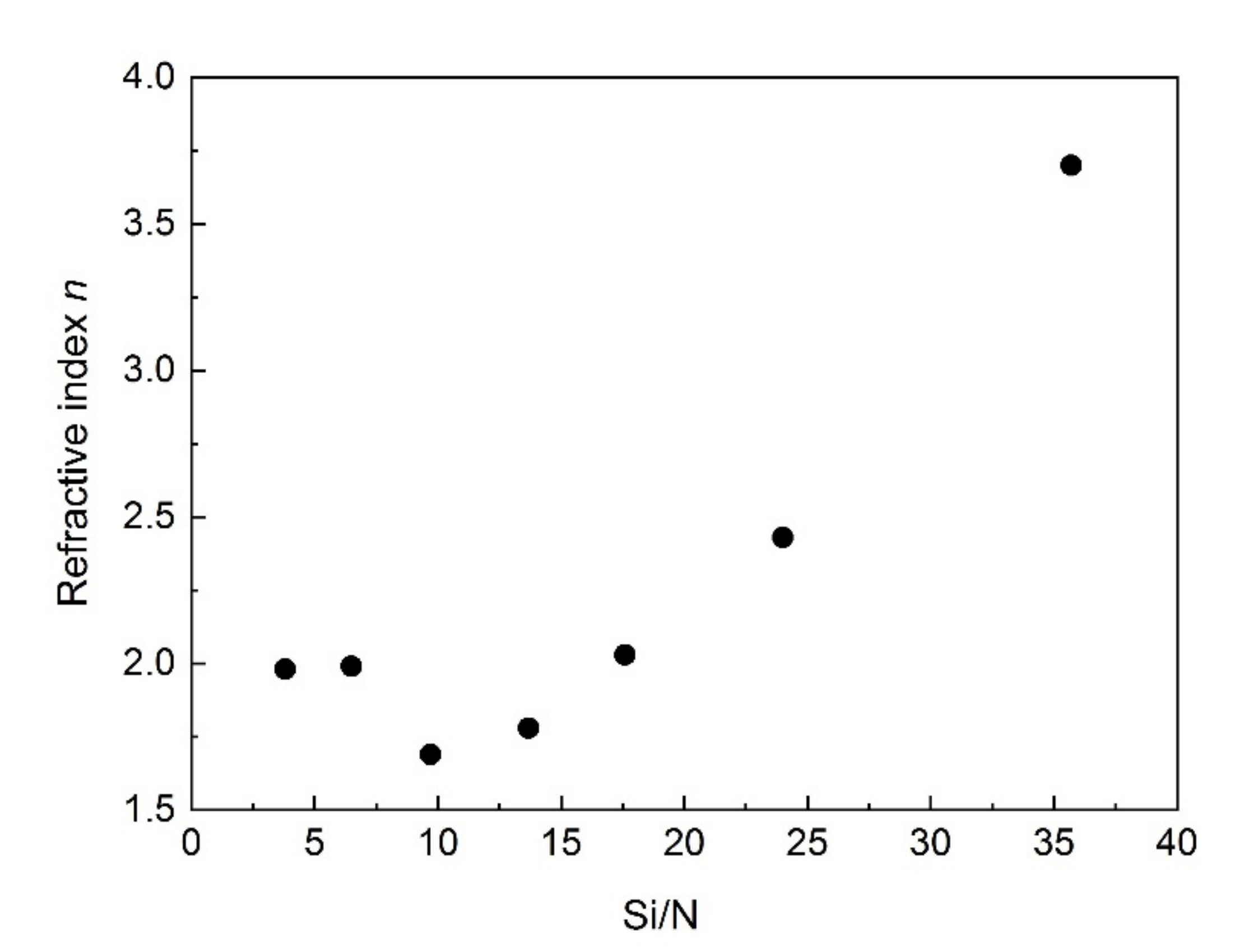
  • Refractive indices of the SiN layers in a wide range from 1.8 to 3.7 strongly depend on the volumetric composition of Si and N components. Measurement results for SiN layers in such a wide range have not been published in the scientific literature so far.
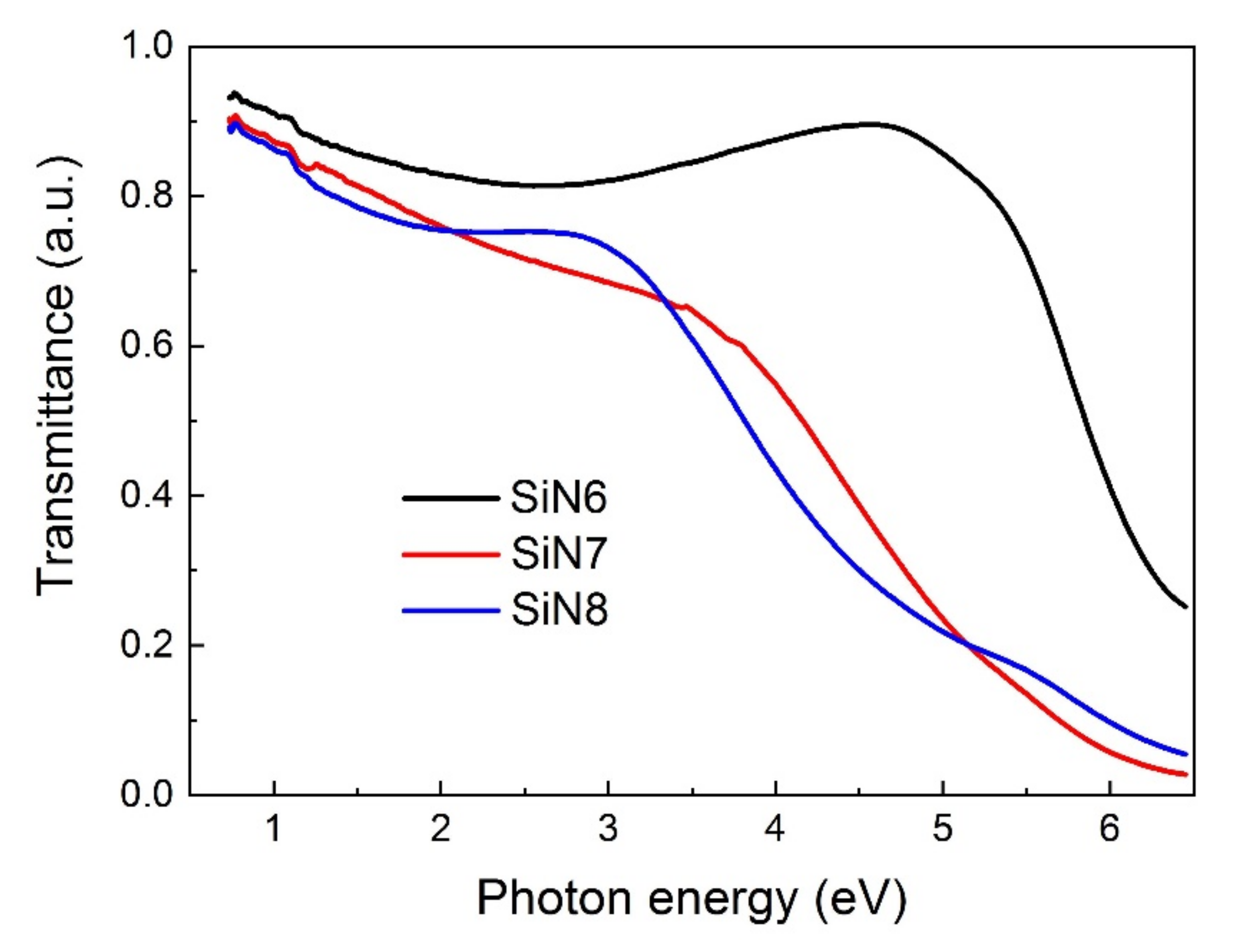
  • The energy gaps of tested SiN layers determined from optical measurements range from 2.22 to 2.25 eV.
From thermal ellipsometric measurements performed for the temperature range of 20 to 300 °C, the spectral dependence and the temperature hysteresis of optical constants were determined. They proved that:
  • Thermo-optical parameters of the SiN layers strongly depended on the technological process.
  • The values of the TOC parameter obtained for the samples prepared with a double frequency of radiation were negative, while the thermo-optical coefficient was positive for SiN layers deposited for one frequency of PACVD radiation.
  • Thermo-optical measurements showed that after annealing up to 300 C and subsequent cooling, the value of optical parameters of layers returned to the initial values, which indicate the reversibility of their thermal properties and thermal stability.

Author Contributions

Conceptualization, J.J., M.J.-S. and S.K.; methodology, N.N., P.D.; software, J.J., N.N.; validation, J.J., M.J.-S. and S.K.; formal analysis, N.N., P.D.; investigation, M.J.-S., S.K., N.N., P.D.; resources, M.J.-S. and S.K.; data curation, M.J.-S., S.K., N.N., P.D.; writing—original draft preparation, J.J., M.J.-S.; writing—review and editing, J.J., M.J.-S. and P.D.; visualization, M.J.-S., N.N., P.D.; supervision, J.J.; funding acquisition, M.J.-S. and S.K. All authors have read and agreed to the published version of the manuscript.

Funding

This research received no external funding.

Institutional Review Board Statement

Not applicable.

Informed Consent Statement

Not applicable.

Data Availability Statement

Not applicable.

Acknowledgments

This work was supported from the subsidy of the Ministry of Education and Science for the AGH University of Science and Technology in Kraków (Project No 16.16.160.557).

Conflicts of Interest

The authors declare no conflict of interest.

Appendix A

Figure A1. SEM images of the surface of the SiN layer illustrating the presence of impurities (a,b) and AFM image of SiN layer (c).
Materials 15 02260 g0a1
Figure A2. EDS analysis performed for point 1 of Figure A1b.
Materials 15 02260 g0a2
Figure A3. X-ray diffraction patterns of the SiN thin films deposited in PECVD system on Si(001).
Materials 15 02260 g0a3

References

  1. Aberle, A.G.; Hezel, R. Progress in low-temperature surface passivation of silicon solar cells using remote-plasma silicon nitride. Prog. Photovolt. 1997, 5, 29–50. [Google Scholar] [CrossRef]
  2. Lipiński, M. Silicon Nitride for Photovoltaic Application. Arch. Mater. Sci. Eng. 2010, 46, 69–87. [Google Scholar]
  3. Dekkers, H.; De Wolf, S.; Agostinelli, G.; Duerinckx, F.; Beaucarne, G. Requirements of PECVD SiNx:H layers for bulk passivation of mc-Si. Sol. Energy Mater. Sol. Cells 2006, 90, 3244–3250. [Google Scholar] [CrossRef]
  4. Lelièvre, J.F.; Kafle, B.; Saint-Cast, P.; Brunet, P.; Magnan, R.; Hernandez, E.; Poliquen, S.; Massines, F. Efficient silicon nitride SiNx:H antireflective and passivation layers deposited by atmospheric pressure PECVD for silicon solar cells. Prog. Photovolt. 2019, 27, 1007–1019. [Google Scholar] [CrossRef]
  5. Aberle, A.G. Surface passivation of crystalline silicon solar cells: A review. Prog. Photovolt. Res. Appl. 2000, 8, 473–487. [Google Scholar] [CrossRef]
  6. Schmidt, J.; Kerr, M. Highest-quality surface passivation of low-resistivity p-type silicon using stiochiometric PECVD silicon nitride. Sol. Energy Mater. Sol. Cells 2001, 65, 585–591. [Google Scholar] [CrossRef] [Green Version]
  7. Lipiński, M.; Panek, P.; Kluska, S.; Zięba, P.; Szyszka, A.; Paszkiewicz, B. Defect passivation of multicrystalline silicon solar cells by silicon nitride coatings. Mater. Sci.-Pol. 2006, 24, 1003–1007. [Google Scholar]
  8. Ghosh, H.; Mitra, S.; Saha, H.; Datta, S.K.; Banerjee, C. Argon plasma treatment of silicon nitride (SiN) for improved antireflection coating on c-Si solar cells. Mater. Sci. Eng. B 2017, 215, 29–36. [Google Scholar] [CrossRef]
  9. Lin, P.T.; Singh, V.; Lin, H.Y.G.; Tiwald, T.; Kimerling, L.C.; Agarwal, A.M. Low-stress Silicon Nitride Platform for Mid-infrared Broadband and Monolithically Integrated Microphotonics. Adv. Opt. Mater. 2013, 1, 732–739. [Google Scholar] [CrossRef]
  10. Nunomura, S.; Sakata, I.; Sato, A.; Lozach, M.; Misawa, T.; Itagaki, N.; Shiratani, M. Passivating antireflection coating of crystalline silicon using i/n a-Si:H/SiNtrilayer. J. Phys. Chem. Sol. 2021, 156, 110127. [Google Scholar] [CrossRef]
  11. Kluska, S.; Hejduk, K.; Drabczyk, K.; Lipiński, M. Optical properties and passivation effects of silicon nitride three layer stack deposited by plasma enhanced chemical vapor deposition. Phys. Status Solidi A 2016, 213, 1839–1847. [Google Scholar] [CrossRef]
  12. Sood, A.K.; Zeller, J.W.; Sood, A.W.; Pethuraja, G.G.; Welser, R.E.; Efstathiadis, H.; Sampath, A.V.; Dhar, N.K. Development of nanostructured antireflection coating for infrared sensing applications. Proc. SPIE 2019, 11129, 111290I. [Google Scholar] [CrossRef]
  13. Yoshinaga, S.; Ishikawa, Y.; Kawamura, Y.; Nakai, Y.; Uraoka, Y. The optical properties of silicon-rich silicon nitride prepared by plasma enhanced chemical vapor deposition. Mater. Sci. Semicond. Proc. 2019, 90, 54–58. [Google Scholar] [CrossRef]
  14. Cho, S.-K.; Cho, T.-Y.; Lee, W.J.; Ryu, J.; Lee, J.H. Structural and gas barrier properties of hydrogenated silicon nitride thin films prepared by roll-to-roll microwave plasma-enhanced chemical vapor deposition. Vacuum 2021, 188, 110167. [Google Scholar] [CrossRef]
  15. Jurzecka-Szymacha, M.; Boszkowicz, P.; Tkacz-Śmiech, K. Silicon nitride layers of various N-content: Technology, properties and structure. Thin Solid Films 2011, 520, 1308–1312. [Google Scholar] [CrossRef]
  16. Song, H.; Seo, S.; Chang, H. Study on SiN and SiCN film production using PE-ALD process with high-density multi-ICP source at low temperature. Curr. Appl. Phys. 2018, 18, 1436–1440. [Google Scholar] [CrossRef]
  17. Thi, T.C.; Koyama, K.; Ohdaira, K.; Matsumura, H. Passivation characteristics of SiNx/a-Si and SiNx/Si-rich-SiNx stacked layers on crystalline silicon. Sol. Energy Mater. Sol. Cells 2012, 100, 169–173. [Google Scholar] [CrossRef]
  18. Sahu, R.; Palei, S.; Choi, J.; Ji, H.Y.; Kim, K. Silicon solar cells with nitrogen-rich SiNx/Si interfacial passivation by low-energy nitrogen-ion implantation. Sol. Energy Mater. Sol. Cells 2021, 220, 110858. [Google Scholar] [CrossRef]
  19. Debieu, O.; Nalini, R.P.; Cardin, J.; Portier, X.; Perrière, J.; Gourbilleau, F. Structural and optical characterization of pure Si-rich nitride thin films. Nanoscale Res. Lett. 2013, 8, 31–44. [Google Scholar] [CrossRef] [Green Version]
  20. Ng, D.K.T.; Wang, Q.; Wang, T.; Ng, S.-K.; Toh, Y.-T.; Lim, K.-P.; Yang, Y.; Tan, D.T.H. Exploring High Refractive Index Silicon-Rich Nitride Films by Low-Temperature Inductively Coupled Plasma Chemical Vapor Deposition and Applications for Integrated Waveguides. Appl. Mater. Interfaces 2015, 7, 21884–21889. [Google Scholar] [CrossRef]
  21. Claassen, W.A.P.; Valkenburg, W.G.J.N.; Willemsen, M.F.C.; Wijgert, W.M.V.D. Influence of deposition temperature, gas pressure, gas phase composition and RF frequency on composition and mechanical stress of plasma silicon nitride layers. J. Electrochem. Soc. 1985, 132, 893–898. [Google Scholar] [CrossRef]
  22. Karouta, F.; Vora, K.; Tian, J.; Jagadish, C. Structural, compositional and optical properties of PECVD silicon nitride layers. J. Phys. D Appl. Phys. 2012, 45, 445301–445311. [Google Scholar] [CrossRef]
  23. Samuelson, G.M.; Mark, M. The correlations between physical and electrical properties of PECVD SiN with their composition ratios. J. Electrochem. Soc. 1982, 129, 1773–1778. [Google Scholar] [CrossRef]
  24. Claassen, W.A.P.; Valkenburg, W.G.J.N.; Habraken, F.H.P.M.; Tamminga, Y. Characterization of Plasma Silicon Nitride Layers. J. Electrochem. Soc. 1983, 130, 2419–2423. [Google Scholar] [CrossRef]
  25. Kim, D.S.; Yoon, S.G.; Jang, G.E.; Suh, S.J.; Kim, H.; Yoon, D.H. Refractive index properties of SiN thin films and fabrication of SiN optical waveguide. J. Electroceramics 2006, 17, 315–318. [Google Scholar] [CrossRef]
  26. Tompkins, H.G.; McGahan, W.A. Spectroscopic Ellipsometry and Reflectometry; Wiley: New York, NY, USA, 1999. [Google Scholar]
  27. Fujiwara, H. Spectroscopic Ellipsometry: Principles and Applications; John Wiley & Sons Ltd.: Hoboken, NJ, USA, 2007. [Google Scholar]
  28. Jellison, G.E.; Modine, F.A. Parameterization of the optical functions of amorphous materials in the interband region. Appl. Phys. Lett. 1996, 69, 371. [Google Scholar] [CrossRef]
  29. Jellison, G.E.; Merkulov, V.I.; Puretzky, A.A.; Geohegan, D.B.; Eres, G.; Lowndes, D.H.; Caughman, J.B. Characterization of thin-film amorphous semiconductors using spectroscopic ellipsometry. Thin Solid Film. 2000, 377–378, 68–73. [Google Scholar] [CrossRef]
  30. Nosidlak, N.; Jaglarz, J.; Danel, A. Ellipsometric studies for thin polymer layers of organic photovoltaic cells. J. Vac. Sci. Technol. B 2019, 37, 062402. [Google Scholar] [CrossRef]
  31. Budai, J.; Hanyecz, I.; Szilágyi, E.; Tóth, Z. Ellipsometric study of SixC films: Analysis of Tauc–Lorentz and Gaussian oscillator models. Thin Solid Film. 2011, 59, 2985–2988. [Google Scholar] [CrossRef]
  32. Kamiya, T.; Nomura, K.; Hosono, H. Electronic structure of the amorphous oxide semiconductor a-InGaZnO4-x: Tauc-Lorentz optical model and origins of subgap states. Phys. Status Solidi A 2009, 206, 860–867. [Google Scholar] [CrossRef]
  33. Woollam, J.A. CompleteEASE™ Data Analysis Manual; JA Woollam Co. Inc.: Lincoln, NE, USA, 2009. [Google Scholar]
  34. Prod’homme, L. A new approach to the thermal change in the refractive index of glasses. Phys. Chem. Glasses 1960, 1, 119–122. [Google Scholar]
  35. Jaglarz, J.; Jurzecka-Szymacha, M.; Kluska, S. Film materials on a-SiNx:H with high refractive index obtained by plasma enhanced chemical vapour deposition technology. Thin Solid Film. 2019, 669, 564–570. [Google Scholar] [CrossRef]
  36. Bustarret, E.; Bensouda, M.; Habrard, M.C.; Bruyère, J.C.; Poulin, S.; Gujrathi, S.C. Configuration statistics in a-SixNyHz alloys: A quantitative bonding analysis. Phys. Rev. B 1988, 38, 8171–8184. [Google Scholar] [CrossRef]
  37. Giorgis, F.; Giuliani, F.; Pirri, C.; Tresso, E.M.; Summonte, C.; Rizzoli, R.; Galloni, R.; Desalvo, A.; Rava, P. Optical, structural and electrical properties of device-quality hydrogenated amorphous silicon-nitride films deposited by plasma-enhanced chemical vapour deposition. Philos. Mag. B 1998, 77, 925–944. [Google Scholar] [CrossRef]
  38. Cheng, Q.; Xu, S.; Ostrikov, K. Controlled-bandgap silicon nitride nanomaterials: Deterministic nitrogenation in high-density plasmas. J. Mater. Chem. 2010, 20, 5853–5859. [Google Scholar] [CrossRef] [Green Version]
  39. Krückel, C.J.; Fülöp, A.; Ye, Z.; Andrekson, P.A.; Torres-Company, V. Optical bandgap engineering in nonlinear silicon nitride waveguides. Opt. Express 2017, 25, 15370–15380. [Google Scholar] [CrossRef] [Green Version]
  40. Li, L.; Feng, X.; Wang, Y.; Guo, M.; Qi, H.; Wei, Z.; Bi, K. Significantly improved measurement accuracy in determining the thermal expansion coefficient of single layer graphene. Diam. Relat. Mater. 2020, 109, 108007. [Google Scholar] [CrossRef]
  41. Liu, Z.; Shen, Z.; Liu, G.; He, L.; Mu, R.; Xu, Z. Sm-doped Gd2Zr2O7 thermal barrier coatings: Thermal expansion coefficient, structure and failure. Vacuum 2021, 190, 110314. [Google Scholar] [CrossRef]
  42. Gumbleton, R.; Cuenca, J.A.; Klemencic, G.M.; Jones, N.; Porch, A. Evaluating the coefficient of thermal expansion of additive manufactured AlSi10Mg using microwave techniques. Addit. Manuf. 2019, 30, 100841. [Google Scholar] [CrossRef]
  43. Jaglarz, J.; Jurzecka-Szymacha, M.; Kluska, S.; Tkacz-Śmiech, K. Thermo-optical properties of high-refractive-index plasma-deposited hydrogenated amorphous silicon-rich nitride films on glass. Opt. Matter. Express 2020, 10, 2749–2756. [Google Scholar] [CrossRef]
Figure 1. Spectral dependence of ellipsometric angles Ψ and Δ for (a) SiN6, (b) SiN7, and (c) SiN8 samples.
Materials 15 02260 g001
Figure 2. Dispersion relations of (a) refractive index n and (b) extinction coefficient k for SiN6, SiN7, and SiN8 samples.
Materials 15 02260 g002
Figure 3. Refractive index as a function of Si/N ratio.
Materials 15 02260 g003
Figure 4. Thermal hysteresis of thickness for SiN6, SiN7, and SiN8 samples at 400 nm.
Materials 15 02260 g004
Figure 5. Thermal hysteresis of refractive index n for (a) SiN6, (b) SiN7, and (c) SiN8 samples.
Materials 15 02260 g005
Figure 6. Thermal hysteresis of extinction coefficient k at 400 nm for SiN6, SiN7, and SiN8 samples.
Materials 15 02260 g006
Figure 7. Dependence of thermo-optical coefficient TOC versus wavelength.
Materials 15 02260 g007
Figure 8. Spectral dependencies of the transmission of SiN6, SiN7, and SiN8 on fused silica.
Materials 15 02260 g008
Table 1. The technological conditions of a-SiNx:H layers deposited in PECVD system.
TechniquePECVD System
Series of SamplesGaseous Substrate Flow [sccm]s = [SiH4]/[NH3]P HF
[W]
Cycletime
[s]
P LF
[W]
Cycle Time
[s]
Substrate Temperature
[C]
Total Time
[s]
NH3SiH4
12940.1341800--2201800
2–520–6040–800.25; 0.42; 0.6; 1;50480--220480
6–895, 20 *, 10 **50, 460 *, 800 **0.5; 23 *; 80 **2040
40 *
144 **
20
20 *
- **
8
8 *
- **
310310
220 *
158 **
* value for sample 7. ** value for sample 8.
Table 2. The value of ratio Si/N for all samples from EDS technique.
SamplesSiN1SiN2SiN3SiN4SiN5SiN6SiN7SiN8SiN9
[Si]/[N]2.283.505.506.509.7013.6817.5824.0035.70
Table 3. Wavenumbers for the principal atom bondings in amorphous silicon nitride [36,37].
Wavenumber (cm−1)BondingAssignment
820–890
1139
2163
3343
Si–N
N–H
Si–H
N–H
Si–N stretching
N–H bending
SiH2 stretching in N3Si–H
N–H in band Si2N–H
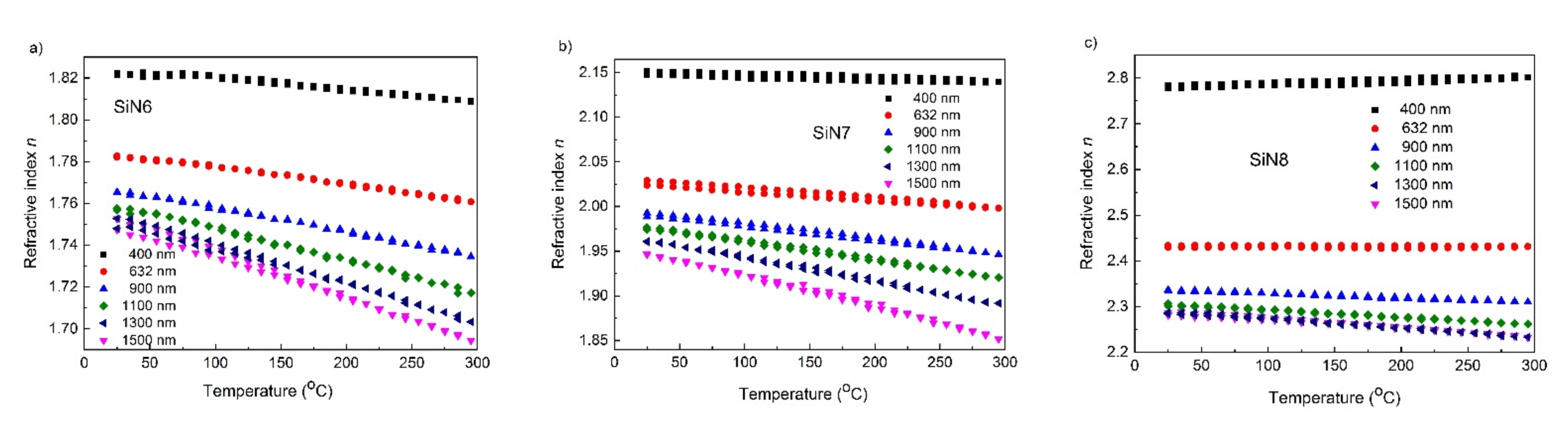
Table 4. Optical parameters and MSE values of SiN6, SiN7, and SiN8 samples.
SampleMSEABEg [eV]n 400 nmn 632 nmn 900 nmn 1500 nm
SiN65.81.160.712.231.821.781.771.75
SiN710.76.160.382.252.152.031.991.95
SiN87.5131.397.222.222.782.432.332.28
Table 5. Thermo-optical coefficient, thermal expansion coefficient and thickness values for SiN6, SiN7, and SiN8 samples.
SampleTOC [10−5/K]Thickness [nm]TEC [10−3 nm/K]
λ
400 [nm]500 [nm]632 [nm]750 [nm]900 [nm]1100 [nm]1300 [nm]1500 [nm]
SiN6−5.16−7.16−8.28−9.87−11.80−15.34−18.84−22.0385.077.04
SiN7−3.17−5.84−9.66−12.50−15.86−20.40−26.33−34.8371.426.12
SiN87.616.95−0.64−4.63−9.72−16.30−20.75−20.6159.736.12
Publisher’s Note: MDPI stays neutral with regard to jurisdictional claims in published maps and institutional affiliations.

