Abstract
The vital role of high-quality-factor (Q) high-frequency (f) dielectric resonators in the growing microwave telecommunication, satellite broadcasting and intelligent transport systems has long motivated the search for new, small size, and lightweight integrated components and packages, prepared by low cost and sustainable processes. One approach is replacing the currently used bulk ceramic dielectrics by thick films of low-sintering-temperature dielectrics fabricated by affordable processes. Here we demonstrate the fabrication of high-Q TiTe3O8 thick films directly on low loss Al2O3 substrates by electrophoretic deposition using sacrificial carbon layer. Nineteen-micrometre-thick TiTe3O8 films on Al2O3 sintered at 700 °C are found to have a relative permittivity εr of 32 and Q × f > 21,000 GHz. Being thus able to measure and provide for the first time the microwave dielectric properties of these films, our results suggest that TiTe3O8 films on Al2O3 substrates are suitable for microlayer microstrip array applications.
1. Introduction
Microwave dielectric materials play a vital role within a wide range of applications from terrestrial and satellite communication including software radio, Global Positioning Systems (GPS), and Direct Broadcast Satellite (DBS) television and environmental monitoring via satellites. The recent progress in microwave telecommunication, satellite broadcasting and intelligent transport systems (ITS) has resulted in an increasing demand for dielectric resonators (DRs), which are low loss ceramic pucks used mainly in wireless communication devices [1]. The key properties required for DR materials are high quality factor-frequency product (Q × f), high relative permittivity (εr) and near zero temperature coefficient of resonant frequency (τf) or temperature coefficient of the relative permittivity (TCεr). The relative permittivity determines the size of the electronic component, the temperature coefficient of resonant frequency establishes the frequency stability, and the loss tangent (tanδ) or quality factor (Q = 1/tanδ) controls the selectivity and performance of the device [2]. An optimal dielectric resonator that satisfies these three properties simultaneously is difficult to achieve solely in a particular material.
In order to meet the specifications of the current and future systems, improved or novel microwave components based on dedicated dielectric materials and new designs are required [3]. In addition, with the recent evolution in mobile phone and satellite communication systems, using microwaves as the carrier, the research and development in the field of device miniaturization is needed [4]. This fast-growing mobile/wireless communication industry is demanding small size and lightweight integrated components and packages at low cost. A method to meet these requirements, which are now under consideration by the community, is the replacement of the currently used bulk ceramic dielectrics by dielectric thick films [4,5].
Electrophoretic deposition (EPD) is one of the processing techniques of thick films. EPD is a colloidal process, in which charged particles dispersed in a stable suspension are driven by electric field to move towards oppositely charged electrodes to build up a particulate coating by deposition on one of the electrodes [3,6,7,8,9,10]. The main advantages of EPD are related to low cost, versatility and ability to coat conformal substrates. However, the utilization of insulating substrates required for low loss microwave applications raises difficulties for the preparation of continuous thick films by EPD, since to apply the electric field during the EPD process the substrate should be a conductor. Moreover, a high corrosion resistance in the EPD suspension and thermal stability are two major criteria that also limit drastically the use of conductive substrates in EPD [7]. This last aspect is of particular relevance when the thick film sintering temperature is high (>1000 °C), thus, restricting considerably the choice of electrodes to high temperature conductive oxides or noble metals, such as gold, platinum and palladium; both expensive alternatives.
There is, however, an approach developed for preparation of thick films by EPD on poorly conducting substrates, using a fugitive layer of graphite [11,12]. Moreover, Y-stabilized zirconia (YSZ) films deposited this way on NiO-YSZ for fuel cell application were reported to be of improved quality. In our previous work, we adapted this approach to the more critical case of EPD films on insulating dielectric substrates (as alumina and glass) for electronic applications [13]. Thin sacrificial layers of conducting carbon were coated onto non-conducting alumina substrates to facilitate the conduction on the substrate surface. The carbon coating burns out during the sintering step, not interfering with the final product. To prove the concept, a layer of high Q ceramic powders of BaNd2Ti5O14 (BNT) was deposited by EPD on the top of the carbon coated alumina. One-hundred-micrometre-thick BNT films on Al2O3 substrates exhibited εr and Q of 146 and 1161 at about 10 GHz when sintered at 1250 °C/1 h. Besides high Q values BNT films on alumina possess high thermal stability and, therefore, are potentially useful for high frequency applications [13]. To date this is the only report on EPD to produce high-Q dielectric thick films on alumina substrates. A limitation of the BaO–Nd2O3–TiO2 system is the high sintering temperature (>1300 °C) required to densify the ceramic bulk or thick layers.
Looking for low sintering temperature dielectrics with low dielectric losses and high capacitance stability tellurium-based systems stand out [14,15,16,17,18,19,20,21,22,23,24,25,26,27,28,29]. Ceramics of Te-based compounds sinter at temperatures under 900 °C [28,29] and exhibit low dielectric losses (Q × f up to 66,000 GHz for Zn2Te3O8 ceramics [23]) and dielectric permittivities ranging from 10.5 for MgTe2O5 [25] to 56 for Bi2TeO6 [16]. The temperature coefficient of resonant frequency varies from −119 ppm/°C for TeO2 [16] to +372 ppm/ °C for BaTiTe3O9 [18]. For well sintered TiTe3O8 ceramics, εr is of 50 and Q × f is of 30,600 GHz at a measurement frequency of 5 GHz [15]. However, there is only one report on the preparation of tellurium-based thick films by EPD [30]. In this paper we reported the low-frequency dielectric properties of the TiTe3O8 films on platinized silicon [30]. Moreover, so far there is no report on the microwave characterization of Te-based thick films neither on their deposition on alumina.
In the present work, we have extended our previous approach of using sacrificial carbon layers for EPD on fully non-conducting substrates, to fabricate for the first time low sintering temperature high Q dielectric Te based thick films on insulator Al2O3 substrates. The dielectric characterization at high frequency suggests that these films are suitable for microlayer microstrip arrays.
2. Materials and Methods
The work here described comprises the following experimental steps: preparation of a stable suspension of TiTe3O8 particles synthesised by solid state reaction, carbon coating of the nonconducting Al2O3 substrates, EPD of green TiTe3O8 thick films on carbon coated Al2O3 substrates and their sintering, as well as electrical characterization of TiTe3O8 thick films on Al2O3 at microwave frequencies.
TiTe3O8 powders were synthesized from reagent-grade TeO2 (>99%, Sigma-Aldrich, Saint Louis, MO, USA) and TiO2 (>99%, Merck KGaA, Darmstadt, Germany) via a conventional solid-state-reaction method, as per [30]. The starting precursors were weighed according to the molar ratio of 3:1, ball mixed with ethanol and dried at 70 °C for 5 h. The mixed powders were calcined at 620 ºC for 50 h and milled for 5 h in a planetary ball mill at 200 rpm using Teflon pots and zirconia balls. Milled TiTe3O8 powders with particle size below 10 μm were ultrasonically dispersed in acetone (>99.5%, Panreac Química SLU, Castellar del Vallès, Spain) with a concentration of 10 g/l. Triethanolamine (TEA) (>99%, Merck KGaA, Darmstadt, Germany) was added as a suspension stabilizer to favour the EPD process [31]. The addition of TEA increased considerably the zeta potential of the suspension to 46.5 mV at pH of 8.1 that guaranteed the fabrication of crack free and homogeneous films. The suspensions were magnetically stirred for 5 h at room temperature. The stability of the suspensions was analysed by transmittance of the UV light (UV-2101/3101PC, Shimadzu Corporation, Kyoto, Japan), particle size distribution and zeta potential techniques (Malvern Zeta sizer Nano ZS, Malvern, Worcestershire, UK).
Non-conducting alumina substrates were coated with a sacrificial conducting carbon film that acts as a temporary electrode being burned at high sintering temperatures without leaving any residual contaminations, as mentioned before. Following our previous work [13], a radio frequency (RF) magnetron sputtering (CRIOLAB, Porto, Portugal) was used to perform the deposition of the carbon layer from the corresponding target (purity > 99.9%, Sofacel Inc., Madrid, Spain) of 55 mm in diameter and 3 mm in thickness on 25.4 × 25.4 × 0.0254 mm3 polycrystalline Al2O3 substrates (99.6%, Coors Ceramics U.K., Glenrothes, Fife, Scotland, UK, with the remaining 0.4 wt. % assumed to be a silicate based sintering aid). The carbon coatings were prepared at a substrate–magnetron distance of 120 mm under Ar pressure of 5.8 × 10⁻³ mbar, with a magnetron current of 0.3 A and a substrate bias of 470 V. The thickness of the carbon layer was controlled by the deposition time.
The carbon coated Al2O3 was employed as a substrate for the deposition of TiTe3O8 films and stainless steel was chosen as the counterpart electrode. EPD was carried out for 3 min under a dc voltage of 100 V from the voltage supply (Glassman High Voltage Inc., High Bridge, NJ, USA). The obtained films were dried for more than 24 h at room temperature and then sintered from 680 °C to 720 °C for 5 h in a closed alumina crucible together with TeO2 powders, to avoid Te volatilization. The use of TeO2 powder was reported to increase the partial pressure of TeO2 and to suppress the evaporation from TiTe3O8 [30].
The crystallographic structure and phase content of TiTe3O8 films were analysed by X-ray diffraction (XRD, PANalytical X’Pert Pro diffractometer, Philips, Amsterdam, The Netherlands, Cu-Kα radiation, 45 kV and 40 mA), used from 10° to 80° 2θ with a step size of 0.025°. The microstructure of the thick films was observed using scanning electron microscopy (SEM, SU-70, Hitachi, Tokyo, Japan) coupled with energy-dispersive X-ray spectroscopy (EDS, QUANTAX 400, Bruker, Billerica, MA, USA). The thickness of green and sintered films was evaluated by a micrometre and SEM.
For microwave frequency characterization the split post dielectric resonator (SPDR) method was used [32]. Thus, εr and quality factor (Q) were determined at ~20 GHz. The method is based on measurements of resonant frequency and quality factor of the empty resonator, the resonator with the substrate (Al2O3), and finally the resonator with dielectric deposited on top of the substrate (in this case TiTe3O8 on Al2O3) with the same exact dimensions and shape. The dielectric parameters of the measured thick dielectric films are calculated based on full-wave electromagnetic analysis.
3. Results
Before alumina substrates are used for EPD, the essential step is to sputter a carbon layer upon it to make them conductive, as explained before. The carbon coatings certainly affect the EPD process and thereby the quality of TiTe3O8 films and their final dielectric performance. According to our previous results, there is an optimum carbon layer thickness in the range between 200 and 400 nm that guarantees a continuous uniform high quality film deposition [13]. Carbon layers with thickness below 100 nm cannot be used as temporary electrodes for EPD since the formed layer is not sufficiently conductive to permit the deposition of a continuous film. On the other hand, with too thick (>500 nm) carbon layers, non-conformal and non-uniform films are obtained after sintering, because thick carbon layers restrict the final film adhesion to the substrate. Therefore, ~300 nm thick carbon layer was selected to be used in the present work.
The surface of the green (non-sintered) TiTe3O8 thick films deposited by EPD under 100 V for 3 min on carbon coated alumina substrate is presented in Figure 1a. Very uniform and crack free TiTe3O8 film with circular shape is seen on the background of the black carbon layer with square shape. The cross-section microstructure of these green films is illustrated in Figure 1 b,d. The low magnification SEM micrograph depicts a very uniform, compact and conformal ~50 µm thick TiTe3O8 film on the carbon coated alumina substrate (Figure 1b,c). TiTe3O8 particles are densely packed and deposited on the substrate thanks to the carbon coating conductive surface. The uniform continuous conformal carbon layer with thickness of ~300 nm can be easily observed from the high magnification micrographs (Figure 1c,d).
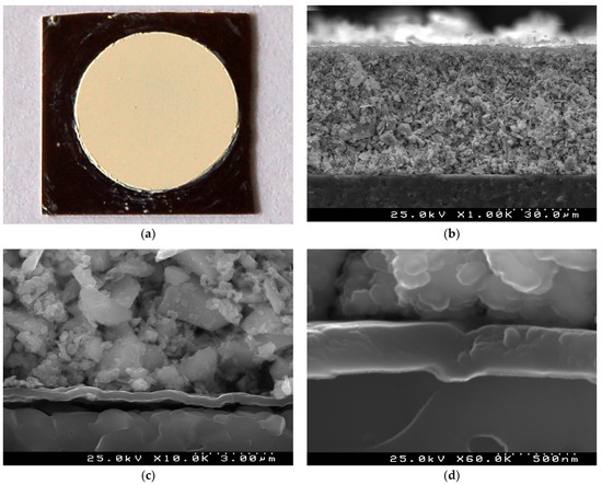
Figure 1.
A surface optical image (a) and cross section SEM micrographs (b–d) of a green TiTe3O8 thick film deposited by EPD under 100 V for 3 min on carbon coated 25.4 × 25.4 × 0.0254 mm3 alumina substrate: very uniform and crack free TiTe3O8 film with a circular shape on a background of a black carbon layer (a), average film thickness of ~50 µm (b) and compact microstructure of the film (c) on a continuous ~300 nm carbon layer (d) are visible.
The optical images of TiTe3O8 films deposited on carbon coated alumina substrates sintered for 5 h in air at 680 (a), 700 (b) and 720 °C (c), respectively, are presented in Figure 2. Sintered TiTe3O8 films exhibit the yellow colour characteristic of polycrystalline TiTe3O8 and the alumina substrates present the original white colour. For films sintered at 680 °C (Figure 2a), the substrate is slightly darker than for the other sintered films. This is possibly due to an incomplete burn out of the sacrificial carbon layer, although thermal analysis (see Appendix A Figure A1) clearly indicates that the carbon layer oxidizes in air below 660 °C and thus below the sintering temperature of TiTe3O8 films. After sintering at 680 °C, films still present a powder-like aspect, similar to the green ones, and do not have good adhesion to the alumina substrates, being easily detached. Therefore, under the present conditions, the sintering temperature of 680 °C is not enough to fully densify TiTe3O8 thick films on Al2O3.
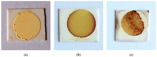
Figure 2.
Optical images of TiTe3O8 films deposited on carbon coated 25.4 × 25.4 × 0.0254 mm3 alumina substrates and sintered at 680 (a), 700 (b) and 720 °C (c) for 5 h, respectively. Films sintered at 680 °C are not fully dense and some films sintered at 720 °C exhibit an irregular surface with a reddish colour resulting from a reaction with the alumina substrate.
Films sintered at higher temperatures, 700 °C and 720 °C, are denser and do not detach from the substrate. However, films sintered at 720 °C exhibit areas with an irregular surface and a reddish colour, as seen from Figure 2c. For films sintered at 700 °C, (Figure 2b) only some reddish vestiges at the edges may be seen. This reddish colour, not observed for the films sintered at 680 °C, may be indicative of some reaction with the alumina substrate. Indeed, in our previous work [33] we proposed that the formation of 1:1 stoichiometry binary Al2O3-TeO2 compound results from the oxidation of TeO2, which occurs at temperatures > 600 °C to form Te4O9 and TeO3, that triggers the formation of Al2TeO6. Under vacuum the oxidation of TeO2 does not take place and there is no reaction between Al2O3 and TeO2.
To understand what gives rise to these observations and to support our predictions we conducted XRD analysis to examine the evolution of the formed phases under different sintering conditions (Figure 3). For the sintering temperature of 680 °C, the XRD pattern reveals only peaks of TiTe3O8 phase (JCPDS 70-2439) identical to those of calcined powders [30]. However, as hypothesised, for films sintered at 700 °C and 720 °C, a new phase of Al2TeO6 (JCPDS 15-0689) can be identified. For films sintered at 700 °C, Al2TeO6 is residual, but for films sintered at 720 °C, Al2TeO6 is clearly visible and even peaks of TiO2 can be detected, indicative of TiTe3O8 decomposition. Thus, the reddish colour observed in TiTe3O8 thick films sintered at temperatures higher than 700 °C is related to the formation Al2TeO6 phase, which results from the reaction between TeO2 from TiTe3O8 and alumina substrates.
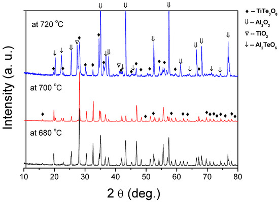
Figure 3.
XRD patterns of TiTe3O8 films deposited on carbon coated alumina substrates and sintered at 680, 700 and 720 °C for 5 h. The main film’s phase is TiTe3O8. For films sintered above 700 °C Al2TeO6 is formed due to a reaction between TeO2 and Al2O3 substrates.
We have also inspected the microstructure of the sintered TiTe3O8 films deposited on carbon coated alumina substrates, for the films sintered at 700 °C for 5 h (Figure 4). Films present a uniform and dense surface microstructure with the typical cubic shaped grains of TiTe3O8 and well visible grain boundaries (Figure 4a). In agreement, a dense microstructure (with only some residual porosity), a thickness of ~19 μm as well as a good adhesion to the substrate can be observed from the cross-section SEM micrographs (Figure 4b). There is also a thin reaction layer between the film and the substrate interface with a thickness of <200 nm (Figure 4c).
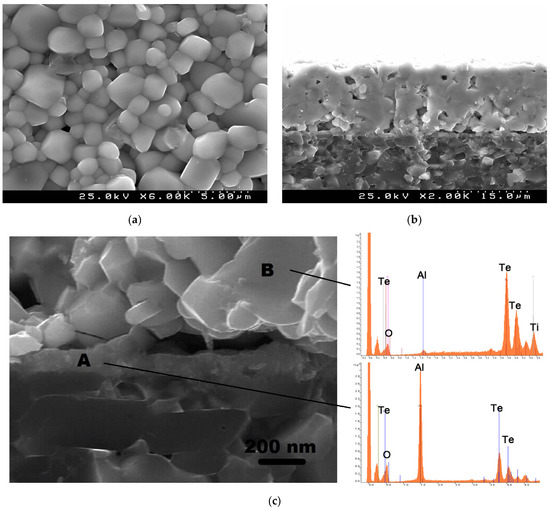
Figure 4.
SEM micrographs of TiTe3O8 films deposited on carbon coated alumina substrates sintered at 700 °C for 5 h, surface (a), cross section (b) and high magnification cross section and energy dispersive spectra for indicated locations (c). Under these sintering conditions (700 °C for 5 h in air) TiTe3O8 films are dense and uniform with the presence of a thin (<200 nm) reaction interlayer of Al2TeO6 confined to the interface between the film and the substrate.
EDS was used for the analysis of the interface between TiTe3O8 films and Al2O3 substrates (Figure 4c). The interlayer at the interface between the film and the substrate (region A) is Al and Te rich, indicating the presence of Al2TeO6 and confirming the previous XRD data. On the other hand, for region B, which corresponds to the main bulk of the thick film, the detected elements are mainly Te and Ti, from TiTe3O8, being the peak for Al considerably low. Thus, under the sintering conditions of 700 °C for 5 h in air rather dense 19-μm-thick TiTe3O8 films are prepared with the presence of a thin (<200 nm) reaction interlayer of Al2TeO6.
The dielectric properties of two most homogeneous and single phase TiTe3O8 thick films on Al2O3 substrates analysed by SPDR method at 20 GHz are presented in Table 1. 21-µm-thick TiTe3O8 films sintered at 680 °C for 5 h display a εr value of 28 and a Q × f value of 21,978, while 19-µm-thick films sintered at 700 °C for 5 h display εr of 32 and Q × f of 21,053. Thus, relative permittivity of TiTe3O8 thick films varies between 28 and 32 and Q × f varies approximately between 21,000 and 22,000. This uncertainty reflects the differences in the density, thickness and possibly the residual presence of the interfacial reaction with Al2O3. Indeed, the dielectric permittivity of the Al2TeO6 interface layer present in films sintered at 700 °C is smaller than that of TiTe3O8 [33]. In a series connection, this should deteriorate the total dielectric properties. However, the negative effect that may be induced by a <200 nm-thick interface layer is apparently compensated by higher density of the films sintered at 700 °C comparing to that of the films sintered at 680 °C.

Table 1.
Relative dielectric permittivity, quality factor–frequency product and losses of TiTe3O8 thick films and ceramics. Sintering conditions are also indicated.
The dielectric performance of TiTe3O8 films on Al2O3 substrates summarized in Table 1 is also compared to that reported for corresponding ceramics at high (GHz) frequencies. It is worthwhile to mention that Q × f for TiTe3O8 thick films have not been reported so far. εr of 50 and Q × f of 30,600 GHz at 5 GHz were reported for TiTe3O8 ceramics sintered at 720 °C [15]. Besides the lower measurement frequency, the observed differences of the dielectric behaviour between TiTe3O8 thick films and ceramics might also be related to density, residual presence of Al2TeO6 secondary phase and details of the microstructure. For other TiTe3O8 ceramics, sintered at 700 °C/5 h, εr and Q at 4 GHz were reported to be 36 and 3400, respectively [14]. Comparing these TiTe3O8 ceramics with our films on Al2O3, the results here obtained are rather promising. Moreover, the low losses of polycrystalline alumina (εr = 9, tanδ = 9.46 × 10⁻⁵, Q = 10570—for > 99% pure Al2O3) [34] should improve the dielectric performance of the final device TiTe3O8/Al2O3 composite structure.
Overall and by comparison, EPD TiTe3O8 thick films on Al2O3 reveal a high performance in terms of permittivity and loss tangent (high Q features) making them promising low-sintering-temperature dielectrics for micron sized high-frequency devices.
4. Conclusions
We have fabricated low-loss (high-Q) TiTe3O8 thick films directly on Al2O3 substrates by EPD and reported for the first time their microwave dielectric properties. Nineteen micrometre-thick TiTe3O8 films on Al2O3 sintered at 700 °C have the relative permittivity of 32 and Q × f > 21,000 GHz at a frequency of 20 GHz. Our results confirm the crucial role of a sacrificial carbon conductive coating on non-conductive Al2O3 substrate for the direct utilization of insulating substrates in EPD. During the sintering of TiTe3O8 films on Al2O3 at temperatures above 700 °C, an interfacial reaction between Al2O3 and TiTe3O8 takes place resulting in the formation of a stable aluminium tellurite compound, Al2TeO6. However, our findings also suggest that this thin (100–200 nm) interlayer of low-loss aluminium tellurite has no significant negative effect on the final properties of TiTe3O8 films. Finally, our results provide relevant information for the use of TiTe3O8 thick films on Al2O3 substrates as microlayer microstrip arrays in antennas, filters and transceivers for microwave telecommunications, satellite broadcasting and intelligent transport systems.
Author Contributions
Conceptualization, P.M.V.; investigation, X.S., A.T. and J.K.; methodology, X.S., A.T., J.K. and P.M.V.; writing—original draft preparation, P.M.V.; writing—review and editing, A.T. and P.M.V.; supervision, P.M.V. All authors have read and agreed to the published version of the manuscript.
Funding
This work was developed within the scope of the project CICECO-Aveiro Institute of Materials, UIDB/50011/2020 and UIDP/50011/2020, financed by national funds through the Portuguese Foundation for Science and Technology/MCTES.
Institutional Review Board Statement
Not applicable.
Informed Consent Statement
Not applicable.
Data Availability Statement
The data presented in this study are available on request from the corresponding author.
Conflicts of Interest
The authors declare no conflict of interest.
Appendix A

Figure A1.
Differential thermal analysis (DTA) and thermogravimetric (TG) analysis curves recorded in air on graphite coated Al2O3 substrate.
Figure A1.
Differential thermal analysis (DTA) and thermogravimetric (TG) analysis curves recorded in air on graphite coated Al2O3 substrate.

References
- Reaney, I.M.; Iddles, D. Microwave Dielectric Ceramics for Resonators and Filters in Mobile Phone Networks. J. Am. Ceram. Soc. 2006, 89, 2063–2072. [Google Scholar] [CrossRef]
- Scott, A.W. Understanding Microwaves; Wiley: New York, NY, USA, 1993. [Google Scholar]
- Vilarinho, P.M.; Fu, Z.; Kingon, A.I.; Tkach, A. Low loss tunable dielectric BaNd2Ti5O14-(Ba0.5Sr0.5)TiO3 composite thick films. Scr. Mater. 2018, 155, 160–163. [Google Scholar] [CrossRef]
- Stephens, D.; Young, P.; Robertson, I. Millimeter-wave substrate integrated waveguides and filters in photoimageable thick-film technology. IEEE Trans. Microw. Theory Tech. 2005, 53, 3832–3838. [Google Scholar] [CrossRef]
- Samanta, K.K. Advanced multilayer thick-film technology and TFMS, CPW, and SIW up to 180 GHz for cost-effective ceramic-based circuits and modules. IET Microw. Antennas Propag. 2018, 12, 1064–1071. [Google Scholar] [CrossRef]
- Sarkar, P.; Nicholson, P.S. Electrophoretic Deposition (EPD): Mechanisms, Kinetics, and Application to Ceramics. J. Am. Ceram. Soc. 1996, 79, 1987–2002. [Google Scholar] [CrossRef]
- Zhitomirsky, I. Cathodic electrodeposition of ceramic and organoceramic materials. Fundamental aspects. Adv. Colloid Interface Sci. 2002, 97, 279–317. [Google Scholar] [CrossRef]
- Besra, L.; Liu, M. A review on fundamentals and applications of electrophoretic deposition (EPD). Prog. Mater. Sci. 2007, 52, 1–61. [Google Scholar] [CrossRef]
- Corni, I.; Ryan, M.P.; Boccaccini, A.R. Electrophoretic deposition: From traditional ceramics to nanotechnology. J. Eur. Ceram. Soc. 2008, 28, 1353–1367. [Google Scholar] [CrossRef]
- Lee, S.H.; Woo, S.P.; Kakati, N.; Kim, D.-J.; Yoon, Y.S. A Comprehensive Review of Nanomaterials Developed Using Electrophoresis Process for High-Efficiency Energy Conversion and Storage Systems. Energies 2018, 11, 3122. [Google Scholar] [CrossRef]
- Basu, R.N.; Randall, C.A.; Mayo, M.J. Fabrication of Dense Zirconia Electrolyte Films for Tubular Solid Oxide Fuel Cells by Electrophoretic Deposition. J. Am. Ceram. Soc. 2001, 84, 33–40. [Google Scholar] [CrossRef]
- Hosomi, T.; Matsuda, M.; Miyake, M. Electrophoretic deposition for fabrication of YSZ electrolyte film on non-conducting porous NiO–YSZ composite substrate for intermediate temperature SOFC. J. Eur. Ceram. Soc. 2007, 27, 173–178. [Google Scholar] [CrossRef]
- Vilarinho, P.M.; Fu, Z.; Wu, A.; Axelsson, A.; Kingon, A.I. Electrophoretic Deposition on Nonconducting Substrates: A Demonstration of the Application to Microwave Devices. Langmuir 2015, 31, 2127–2135. [Google Scholar] [CrossRef]
- Maeda, M.; Yamamura, T.; Ikeda, T. Dielectric Characteristics of Several Complex Oxide Ceramics at Microwave Frequencies. Jpn. J. Appl. Phys. 1987, 26, 76–79. [Google Scholar] [CrossRef]
- Udovic, M.; Valant, M.; Suvorov, D. Dielectric characterisation of ceramics from the TiO2–TeO2 system. J. Eur. Ceram. Soc. 2001, 21, 1735–1738. [Google Scholar] [CrossRef]
- Udovic, M.; Valant, M.; Suvorov, D. Phase Formation and Dielectric Characterization of the Bi2O3-TeO2 System Prepared in an Oxygen Atmosphere. J. Am. Ceram. Soc. 2004, 87, 591–597. [Google Scholar] [CrossRef]
- Valant, M.; Suvorov, D. Glass-free low-temperature cofired ceramics: Calcium germanates, silicates and tellurates. J. Eur. Ceram. Soc. 2004, 24, 1715–1719. [Google Scholar] [CrossRef]
- Kwon, D.-K.; Lanagan, M.T.; Shrout, T.R. Synthesis of BaTiTe3O9 Ceramics for LTCC Application and Its Dielectric Properties. J. Ceram. Soc. Jpn. 2005, 113, 216–219. [Google Scholar] [CrossRef][Green Version]
- Kwon, D.-K.; Lanagan, M.T.; Shrout, T.R. Microwave Dielectric Properties and Low-Temperature Cofiring of BaTe4O9 with Aluminum Metal Electrode. J. Am. Ceram. Soc. 2005, 88, 3419–3422. [Google Scholar] [CrossRef]
- Udovic, M.; Valant, M.; Jančar, B.; Suvorov, D.; Meden, A.; Kočevar, A. Phase Formation and Crystal-Structure Determination in the Bi2O3–TiO2–TeO2 System Prepared in an Oxygen Atmosphere. J. Am. Ceram. Soc. 2006, 89, 3462–3469. [Google Scholar] [CrossRef]
- Udovic, M.; Suvorov, D. Sintering and Dielectric Characterization of Pseudoternary Compounds from the Bi2O3–TiO2–TeO2 System. J. Am. Ceram. Soc. 2007, 90, 2404–2408. [Google Scholar] [CrossRef]
- Kwon, D.-K.; Lanagan, M.T.; Shrout, T.R. Microwave dielectric properties of BaO–TeO2 binary compounds. Mater. Lett. 2007, 61, 1827–1831. [Google Scholar] [CrossRef]
- Subodh, G.; Sebastian, M.T. Glass-Free Zn2Te3O8 Microwave Ceramic for LTCC Applications. J. Am. Ceram. Soc. 2007, 90, 2266–2268. [Google Scholar] [CrossRef]
- Subodh, G.; Sebastian, M.T. Microwave Dielectric Properties of ATe3O8 (A = Sn, Zr) Ceramics. Jpn. J. Appl. Phys. 2008, 47, 7943–7946. [Google Scholar] [CrossRef]
- Subodh, G.; Ratheesh, R.; Jacob, M.; Sebastian, M. Microwave dielectric properties and vibrational spectroscopic analysis of MgTe2O5 ceramics. J. Mater. Res. 2008, 23, 1551–1556. [Google Scholar] [CrossRef]
- Wang, S.-F.; Wang, Y.-R.; Hsu, Y.-F.; Tsai, J.-S. Densification, microstructure and microwave dielectric properties of ultra-low fire BaTe4O9–TiTe3O8 ceramic composites. J. Eur. Ceram. Soc. 2010, 30, 1737–1741. [Google Scholar] [CrossRef]
- Jiao, X.; Zhong, C.; Zhang, S.; Liu, X.; Li, B. Microwave dielectric properties of BaO–TiO2–TeO2 ternary system. J. Mater. Sci. 2010, 45, 3331–3335. [Google Scholar] [CrossRef]
- Kagomiya, I.; Kodama, Y.; Shimizu, Y.; Kakimoto, K.-I.; Ohsato, H.; Miyauchi, Y. Low-temperature sintering and microwave dielectric properties of Al2TeO6–TeO2 ceramics. J. Alloy. Compd. 2015, 640, 383–387. [Google Scholar] [CrossRef]
- Sebastian, M.T.; Wang, H.; Jantunen, H. Low temperature co-fired ceramics with ultra-low sintering temperature: A review. Curr. Opin. Solid State Mater. Sci. 2016, 20, 151–170. [Google Scholar] [CrossRef]
- Su, X.; Wu, A.; Vilarinho, P.M. Titanium tellurite thick films prepared by electrophoretic deposition and their dielectric properties. Scr. Mater. 2009, 61, 536–539. [Google Scholar] [CrossRef]
- Su, X.; Wu, A.; Vilarinho, P.M. Triethanolamine as an Additive in the Electrophoretic Deposition of TiTe3O8 Thick Films. Key Eng. Mater. 2012, 507, 27–34. [Google Scholar] [CrossRef]
- Krupka, J. Microwave Measurements of Electromagnetic Properties of Materials. Materials 2021, 14, 5097. [Google Scholar] [CrossRef] [PubMed]
- Su, X.; Wu, A.; Vilarinho, P.M. Al2TeO6: Mechanism of phase formation and dielectric properties. Scr. Mater. 2012, 67, 927–930. [Google Scholar] [CrossRef]
- Thorp, J.S.; Akhtaruzzaman, M.; Evans, D. The dielectric properties of alumina substrates for microelectronic packaging. J. Mater. Sci. 1990, 25, 4143–4149. [Google Scholar] [CrossRef]


Publisher’s Note: MDPI stays neutral with regard to jurisdictional claims in published maps and institutional affiliations. |
© 2022 by the authors. Licensee MDPI, Basel, Switzerland. This article is an open access article distributed under the terms and conditions of the Creative Commons Attribution (CC BY) license (https://creativecommons.org/licenses/by/4.0/).