
High-κ van der Waals Oxide MoO3 as Efficient Gate Dielectric for MoS2 Field-Effect Transistors


Abstract
:1. Introduction
2. Results and Discussion
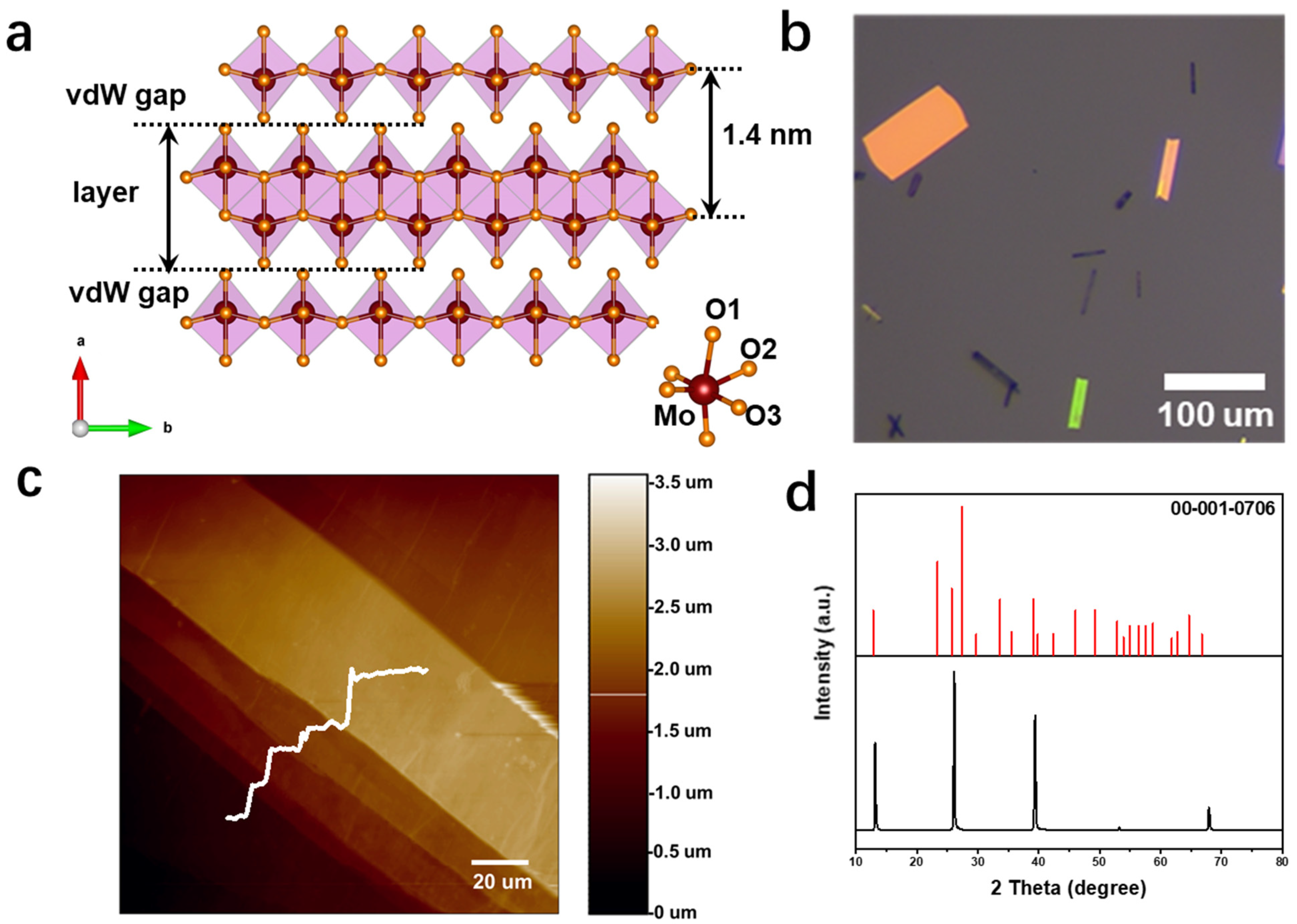
2.1. Structural Characteristics of α-MoO3 Flakes
2.2. Device Performance
2.3. Device Mechanism Exploration
2.4. Device Specific Performance Parameters
3. Conclusions
4. Experimental Section
Supplementary Materials
Author Contributions
Funding
Conflicts of Interest
References
- Robertson, J.; Falabretti, B. Band offsets of high K gate oxides on III-V semiconductors. J. Appl. Phys. 2006, 100, 014111. [Google Scholar] [CrossRef]
- Javey, A.; Kim, H.; Brink, M.; Wang, Q.; Ural, A.; Guo, J.; McIntyre, P.; McEuen, P.; Lundstrom, M.; Dai, H. High-kappa dielectrics for advanced carbon-nanotube transistors and logic gates. Nat. Mater. 2002, 1, 241–246. [Google Scholar] [CrossRef] [PubMed]
- Gusev, E.P.; Cartier, E.; Buchanan, D.A.; Gribelyuk, M.; Copel, M.; Okorn-Schmidt, H.; D’Emic, C. Ultrathin high-K metal oxides on silicon: Processing, characterization and integration issues. Microelectron. Eng. 2001, 59, 341–349. [Google Scholar] [CrossRef]
- Wilk, G.D.; Wallace, R.M.; Anthony, J.M. High-κ gate dielectrics: Current status and materials properties considerations. J. Appl. Phys. 2001, 89, 5243–5275. [Google Scholar] [CrossRef]
- Wang, Y.; Chhowalla, M. Making clean electrical contacts on 2D transition metal dichalcogenides. Nat. Rev. Phys. 2022, 4, 101–112. [Google Scholar] [CrossRef]
- Chourasia, N.K.; Sharma, A.; Acharya, V.; Pal, N.; Biring, S.; Pal, B.N. Solution processed low band gap ion-conducting gate dielectric for low voltage metal oxide transistor. J. Alloys Compd. 2019, 777, 1124–1132. [Google Scholar] [CrossRef]
- Ganapathi, K.L.; Bhat, N.; Mohan, S. Optimization and integration of ultrathin e-beam grown HfO2 gate dielectrics in MoS2 transistors. J. Phys. D Appl. Phys. 2021, 54, 445302. [Google Scholar] [CrossRef]
- Cho, A.J.; Yang, S.; Park, K.; Namgung, S.D.; Kim, H.; Kwon, J.Y. Multi-Layer MoS2 FET with Small Hysteresis by Using Atomic Layer Deposition Al2O3 as Gate Insulator. ECS Solid State Lett. 2014, 3, Q67–Q69. [Google Scholar] [CrossRef]
- Ahmed, F.; Heo, S.; Yang, Z.; Ali, F.; Ra, C.H.; Lee, H.-I.; Taniguchi, T.; Hone, J.; Lee, B.H.; Yoo, W.J. Dielectric Dispersion and High Field Response of Multilayer Hexagonal Boron Nitride. Adv. Funct. Mater. 2018, 28, 1804235. [Google Scholar] [CrossRef]
- Liu, K.; Jin, B.; Han, W.; Chen, X.; Gong, P.; Huang, L.; Zhao, Y.; Li, L.; Yang, S.; Hu, X.; et al. A wafer-scale van der Waals dielectric made from an inorganic molecular crystal film. Nat. Electron. 2021, 4, 906–913. [Google Scholar] [CrossRef]
- Khandare, L.; Terdale, S.S.; Late, D.J. Ultra-fast α-MoO3 nanorod-based Humidity sensor. Adv. Device Mater. 2016, 2, 15–22. [Google Scholar] [CrossRef]
- Holler, B.A.; Crowley, K.; Berger, M.H.; Gao, X.P.A. 2D Semiconductor Transistors with Van der Waals Oxide MoO3 as Integrated High-κ Gate Dielectric. Adv. Electron. Mater. 2020, 6, 2000635. [Google Scholar] [CrossRef]
- Bhattacharjee, S.; Ganapathi, K.L.; Mohan, S.; Bhat, N. A sub-thermionic MoS2 FET with tunable transport. Appl. Phys. Lett. 2017, 111, 163501. [Google Scholar] [CrossRef]
- Chau, T.K.; Phan, T.L.; Park, N.; Na, J.; Suh, D. Distinctive Photo-Induced Memory Effect in Heterostructure of 2D Van Der Waals Materials and Lanthanum Aluminate. Adv. Opt. Mater. 2022, 10, 2200124. [Google Scholar] [CrossRef]
- Guo, Y.; Robertson, J. Origin of the high work function and high conductivity of MoO3. Appl. Phys. Lett. 2014, 105, 222110. [Google Scholar] [CrossRef]
- Peelaers, H.; Chabinyc, M.L.; Van de Walle, C.G. Controlling n-Type Doping in MoO3. Chem. Mater. 2017, 29, 2563–2567. [Google Scholar] [CrossRef]
- Meyer, J.; Kidambi, P.R.; Bayer, B.C.; Weijtens, C.; Kuhn, A.; Centeno, A.; Pesquera, A.; Zurutuza, A.; Robertson, J.; Hofmann, S. Metal oxide induced charge transfer doping and band alignment of graphene electrodes for efficient organic light emitting diodes. Sci. Rep. 2014, 4, 5380. [Google Scholar] [CrossRef]
- Wang, Y.; Du, X.; Wang, J.; Su, M.; Wan, X.; Meng, H.; Xie, W.; Xu, J.; Liu, P. Growth of Large-Scale, Large-Size, Few-Layered alpha-MoO3 on SiO2 and Its Photoresponse Mechanism. ACS Appl. Mater. Interfaces 2017, 9, 5543–5549. [Google Scholar] [CrossRef] [PubMed]
- Bai, J.; Huang, Y. Fabrication and electrical properties of graphene nanoribbons. Mater. Sci. Eng. R Rep. 2010, 70, 341–353. [Google Scholar] [CrossRef]
- Ferrari, A.C.; Meyer, J.C.; Scardaci, V.; Casiraghi, C.; Lazzeri, M.; Mauri, F.; Piscanec, S.; Jiang, D.; Novoselov, K.S.; Roth, S.; et al. Raman spectrum of graphene and graphene layers. Phys. Rev. Lett. 2006, 97, 187401. [Google Scholar] [CrossRef] [Green Version]
- Li, H.; Zhang, Q.; Yap, C.C.R.; Tay, B.K.; Edwin, T.H.T.; Olivier, A.; Baillargeat, D. From Bulk to Monolayer MoS2: Evolution of Raman Scattering. Adv. Funct. Mater. 2012, 22, 1385–1390. [Google Scholar] [CrossRef]
- Seguin, L.; Figlarz, M.; Cavagnat, R.; Lassègues, J.C. Infrared and Raman spectra of MoO3 molybdenum trioxides and MoO3 · xH2O molybdenum trioxide hydrates. Spectrochim. Acta Part A Mol. Biomol. Spectrosc. 1995, 51, 1323–1344. [Google Scholar] [CrossRef]
- Crowley, K.; Ye, G.; He, R.; Abbasi, K.; Gao, X.P. α-MoO3 as a conductive 2D oxide: Tunable n-type electrical transport via oxygen vacancy and fluorine doping. ACS Appl. Nano Mater. 2018, 1, 6407–6413. [Google Scholar] [CrossRef]
- Liu, D.; Guo, Y.; Fang, L.; Robertson, J. Sulfur vacancies in monolayer MoS2 and its electrical contacts. Appl. Phys. Lett. 2013, 103, 183113. [Google Scholar] [CrossRef]
- Srivastava, A.; Fahad, M.S. Vertical MoS2/hBN/MoS2 interlayer tunneling field effect transistor. Solid State Electron. 2016, 126, 96–103. [Google Scholar] [CrossRef]
- Hu, Y.; Jiang, H.; Lau, K.M.; Li, Q. Chemical vapor deposited monolayer MoS2 top-gate MOSFET with atomic-layer-deposited ZrO2 as gate dielectric. Semicond. Sci. Technol. 2018, 33, 045004. [Google Scholar] [CrossRef]


| Gate Material with MoS2 | hBN [25] | ZrO2 [26] | Al2O3 [8] | HfO2 [7] | Sb2O3 [10] | MoO3 (This Work) |
|---|---|---|---|---|---|---|
| Thickness (nm) | 7 | 27 | 100 | 5 | 40 | 90 |
| Threshold voltage (V) | −2 | −6 | −1 | −1 | −7 | −1 |
| Current switching ratio | 103 | 105 | 106 | 106 | 108 | 105 |
| Electron mobility (cm2 V−1 s−1) | 45 | 6.9~11.5 | 200 | 8 | 70~90 | 85 |
| Trap states density (cm−2) | 1.9 × 10¹¹ | 3 × 10¹² | - | 1 × 10¹³ | 6.9 × 10⁹ | 9.8 × 10¹⁰ |
| SS (mV/dec) | 57 | 276 | - | 110~120 | - | 400 |
Publisher’s Note: MDPI stays neutral with regard to jurisdictional claims in published maps and institutional affiliations. |
© 2022 by the authors. Licensee MDPI, Basel, Switzerland. This article is an open access article distributed under the terms and conditions of the Creative Commons Attribution (CC BY) license (https://creativecommons.org/licenses/by/4.0/).
Share and Cite
Wang, J.; Lai, H.; Huang, X.; Liu, J.; Lu, Y.; Liu, P.; Xie, W. High-κ van der Waals Oxide MoO3 as Efficient Gate Dielectric for MoS2 Field-Effect Transistors. Materials 2022, 15, 5859. https://doi.org/10.3390/ma15175859
Wang J, Lai H, Huang X, Liu J, Lu Y, Liu P, Xie W. High-κ van der Waals Oxide MoO3 as Efficient Gate Dielectric for MoS2 Field-Effect Transistors. Materials. 2022; 15(17):5859. https://doi.org/10.3390/ma15175859
Chicago/Turabian StyleWang, Junfan, Haojie Lai, Xiaoli Huang, Junjie Liu, Yueheng Lu, Pengyi Liu, and Weiguang Xie. 2022. "High-κ van der Waals Oxide MoO3 as Efficient Gate Dielectric for MoS2 Field-Effect Transistors" Materials 15, no. 17: 5859. https://doi.org/10.3390/ma15175859
APA StyleWang, J., Lai, H., Huang, X., Liu, J., Lu, Y., Liu, P., & Xie, W. (2022). High-κ van der Waals Oxide MoO3 as Efficient Gate Dielectric for MoS2 Field-Effect Transistors. Materials, 15(17), 5859. https://doi.org/10.3390/ma15175859