Article

Chemical Reaction and Ion Bombardment Effects of Plasma Radicals on Optoelectrical Properties of SnO2 Thin Films via Atomic Layer Deposition

1
School of Information Engineering, Jimei University, Jimei District, Xiamen 361021, China
2
School of Opto-Electronic and Communication Engineering, Xiamen University of Technology, Xiamen 361024, China
3
Department of Materials Science and Engineering, Da-Yeh University, Dacun, Changhua 51591, Taiwan
4
Department of Applied Physics, National University of Kaohsiung, Kaohsiung University Road, Kaohsiung 81148, Taiwan
5
Fujian Key Laboratory of Optoelectronic Technology and Devices, Xiamen University of Technology, Xiamen 361024, China
*
Authors to whom correspondence should be addressed.
Materials 2021, 14(3), 690; https://doi.org/10.3390/ma14030690
Submission received: 29 November 2020 / Revised: 11 January 2021 / Accepted: 26 January 2021 / Published: 2 February 2021
(This article belongs to the Special Issue Atomic Layer Deposition Technique in Material Science)

Abstract

:
In this study, the effect of radical intensity on the deposition mechanism, optical, and electrical properties of tin oxide (SnO2) thin films is investigated. The SnO2 thin films are prepared by plasma-enhanced atomic layer deposition with different plasma power from 1000 to 3000 W. The experimental results show that plasma contains different amount of argon radicals (Ar*) and oxygen radicals (O*) with the increased power. The three deposition mechanisms are indicated by the variation of Ar* and O* intensities evidenced by optical emission spectroscopy. The adequate intensities of Ar* and O* are obtained by the power of 1500 W, inducing the highest oxygen vacancies (OV) ratio, the narrowest band gap, and the densest film structure. The refractive index and optical loss increase with the plasma power, possibly owing to the increased film density. According to the Hall effect measurement results, the improved plasma power from 1000 to 1500 W enhances the carrier concentration due to the enlargement of OV ratio, while the plasma powers higher than 1500 W further cause the removal of OV and the significant bombardment from Ar*, leading to the increase of resistivity.

1. Introduction

In the past few decades, tin oxide (SnO2), as a promising semiconductor material, has gained significant attention due to the excellent photoelectric properties, such as high transparency, suitable band gap and band structure, and superior electron mobility. In recent works, there are abundant techniques to prepare the SnO2 thin films, including magnetron sputter deposition (MSD) [1,2,3,4], thermal evaporation [5], spray pyrolysis deposition [6,7], sol–gel process [8,9,10,11], and chemical vapor deposition (CVD) [12,13,14,15]. However, these technologies still have many shortcomings such as poor coverage, presence of pinholes, and the uncontrolled defects. The atomic layer deposition (ALD) has become a proper candidate to improve the above-mentioned hindrances due to high volatility of precursors, lower process temperature, and pinhole-free deposition at atomic scale. Therefore, the ALD has been widely harnessed in the innovative optoelectronics devices, such as sensors [16], batteries [17], transistors [18], solar cells [19,20], light-emitting diode [20], and flexible electronic devices [21]. At the same time, plasma-enhanced ALD (PEALD) not only enhances the coverage of layer-by-layer at the atomic scale in ALD, but facilitates the production of uniform, dense, and conformal films. Comparable to what has been accomplished for ALD, the challenge for PEALD regards the effects of plasma radicals on the deposition mechanism and the quality of deposited SnO2 thin films. With the development of plasma assistance for the deposition, there are an increasing number of articles about high-quality PEALD SnO2 films [22,23,24,25,26]. On the other hand, the SnO2 thin films have been widely used in many applications such as gas sensors [16], photovoltaics [19,20], and photodetectors [20]. In particular, the SnO2 thin films recently demonstrate great potential for the use as electrical transport layer of perovskite solar cells [19,23]. PEALD is a promising thin-film deposition technique owing to its pinhole-free deposition, ability to control thickness at atomic level, and high conformality on 3D substrates. However, the influences of plasma radicals on the surface reactions and film properties are rarely reported. It is known that the photoelectric properties of SnO2 thin films greatly depend on the intrinsic defects which are formed during the deposition process. As one of the major defects, some studies reported that the presence of oxygen vacancy defects may lead a trade-off between the loss in optical properties and the gain in electrical properties of the SnO2 [7,27,28,29,30], and thus the control of the oxygen vacancy defects depends on applications. It is necessary to acquire a balance between optical and electrical consideration. Owing to the high reactivity, the oxygen gas (O2) is one of the most used sources to generate oxygen radicals, assisting the chemical reaction in PEALD process. Accordingly, it is found that PEALD, playing a crucial role in high quality of SnO2 thin films, is worth researching deeply because the coordination of oxygen vacancies is related to the intensity of oxygen radicals [24]. Therefore, the target of this study is to optimize the PEALD O2 plasma power and investigate its effect on the SnO2 thin film properties. This study is helpful for preparing high-quality SnO2 to be used in perovskite solar cells.
Here, the preparation for PEALD SnO2 thin films at different plasma power from 1000 to 3000 W is studied. Both argon gas (Ar) and O2 are ionized to plasma as reactant to react with the used metal precursor of tetrakis(dimethylamino)tin (TDMA-Sn). The effects of radical intensity on the deposition mechanism, optical, and electrical properties of the SnO2 thin films are investigated to discuss the relationship between oxygen vacancies and radicals.

2. Materials and Methods

2.1. Materials and PEALD Process

The SnO2 thin films were deposited by PEALD (R200, Picosun, Suzhou, China), where the remote plasma is equipped by inductively coupled coil with radio frequency of 13.56 MHz. The power of the PEALD is purchased from Applied Energy, USA with the reflected power of zero. The Ar (99.999%) and O2 (99.999%) mixture is ionized into plasma. The used substrates are glass of soda-lime glass (Asahi, Tokyo, Japan) with a thickness of 0.2 mm and a size of 3 × 3 cm, and p-type silicon wafer with (100). The used precursor of Sn source was TDMA-Sn (C8H24N4Sn, 99.9999%, Nanjing Ai Mou Yuan Scientific Equipment, Nanjing, China) maintained in the bubbler at 50 °C in PEALD process. The Si and glass substrate were cleaned in an ultrasonic bath with deionized water, acetone, and ethanol for 15 min, and then dried with nitrogen gas (N2) and in an oven at 70 °C for 30 min. The substrates were placed on the substrate holder in the deposition chamber of PEALD. In the PEALD process, the substrate temperature was kept at 300 °C and the plasma power was varied from 1000 to 3000 W. The first deposition cycle consisted of following steps: the TDMA-Sn pulse of 1.6 s and then the N2 (99.99%) purging of 6 s. Then, before the N2 purging, plasma exposure of 5 s. The N2 of 120 sccm was used as the carrier gas to bring out the TDMA-Sn vapors, which were then diluted by a 400 sccm N2 gas before entering the chamber. Afterwards, the deposition chamber was pumped to 10−4 Torr before introducing the O/Ar gas mixture. The plasma was generated by the Ar as carrier gas of 80 sccm and O2 of 150 sccm with 11 s into the reaction chamber. The N2 purging gas thus should not influence the O/Ar plasma.

2.2. Characteristic Measurements

Five samples were prepared for each plasma power. Both thickness (d) and refractive index (n) of the SnO2 thin films were determined by using an ellipsometer (M-2000, J. A. Woollam Co., Inc., Lincoln, NE, USA) to estimate the deposition rate. The error estimation of the d was less than ±2%, indicating a good reproducibility. For the ellopsometric data, the films were prepared on a silicon wafer, and a model consisting of “air, air/SnO2, SnO2, SnO2/silicon” was used, where the SnO2 layer was fitted using Drude–Lorentz model. The optical properties of all samples were measured in the wavelength range of 350 to 850 nm via the ultraviolet–visible spectroscopy (MFS-630, Hong-Ming Technology, New Taipei, Taiwan). The plasma radical intensities were obtained by the optical emission spectroscopy (OES, SD2048DL, Verity, Carrollton, TX, USA) from 350 to 800 nm. The peaks at 696.3, 706.8, 738.3, 750.3, 763.5, 772.3, and 794.8 nm are assigned to the Ar* lines [31,32,33,34], while the peak at 777 nm is designated to the O* line [31,32,33,34]. The Ar* lines intensities are summed and illustrated in Figure 1b (together with the O* line intensity). The OES spectra were measured through a quartz optical window, which has very low absorption coefficients in the visible light range and thus has little influence on the measurement. The ratio of oxygen vacancies (OV) to oxygen lattice (OL) was calculated by the results of peak-differentiating and imitating for the O 1s core level obtained by X-ray photoelectron spectroscopy (XPS, ESCALAB, 250Xi, Thermo Fisher, Waltham, MA, USA). The samples were sputtered before XPS measurement to remove surface contamination. The XPS spectra were calibrated by C 1s (284.5 eV). The peak value of OV was located at 532 ± 0.1 eV and that of OL were located at 531 ± 0.1 eV [24,25,26]. The Sn 3d peak for the films prepared at different plasma powers are added as shown in Figure S1. The Sn 3d curves are deconvoluted into two components of Sn4+ and Sn2+. The higher binding energy component at ~487.5 eV is attributed to the Sn4+, while the lower one at ~486.4 eV is typically assigned to Sn2+ [24,25,26]. The electrical properties including the resistivity, carrier concentration, and mobility were conducted by Hall effect measurements (HMS-5000, Side Semiconductor Technology, Xiamen, China) at room temperature. The resistivity of all samples was further illustrated with 4-point probe (T200OA2, Ossila, Sheffield, UK).

3. Results and Discussion

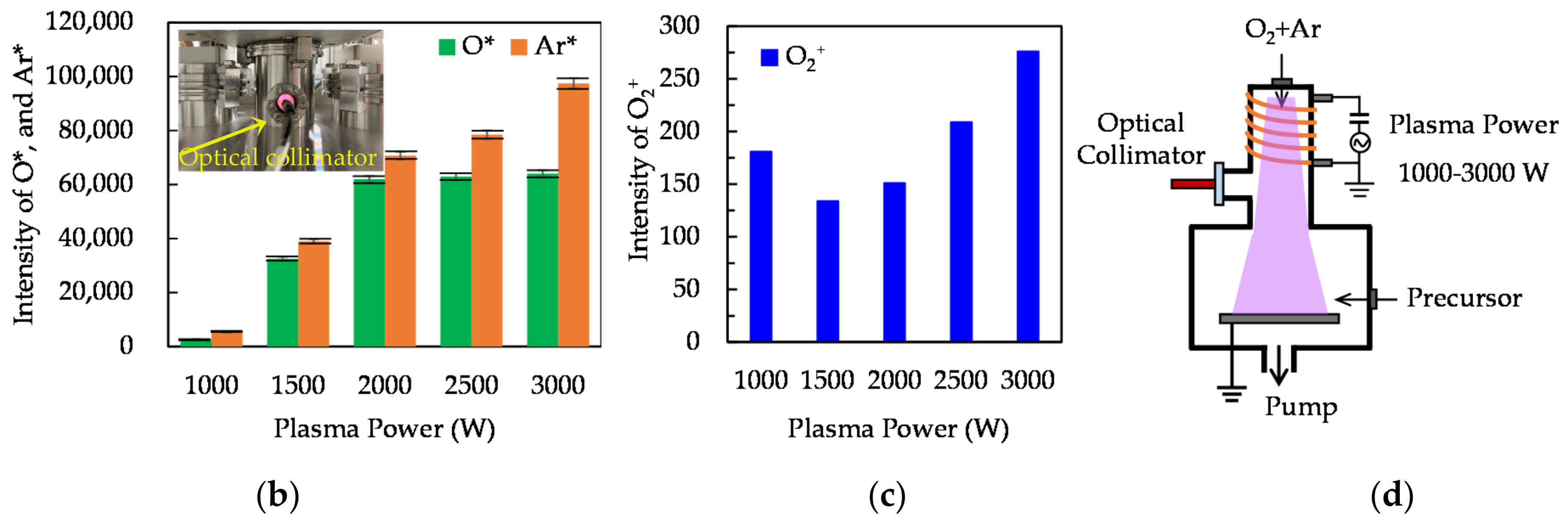
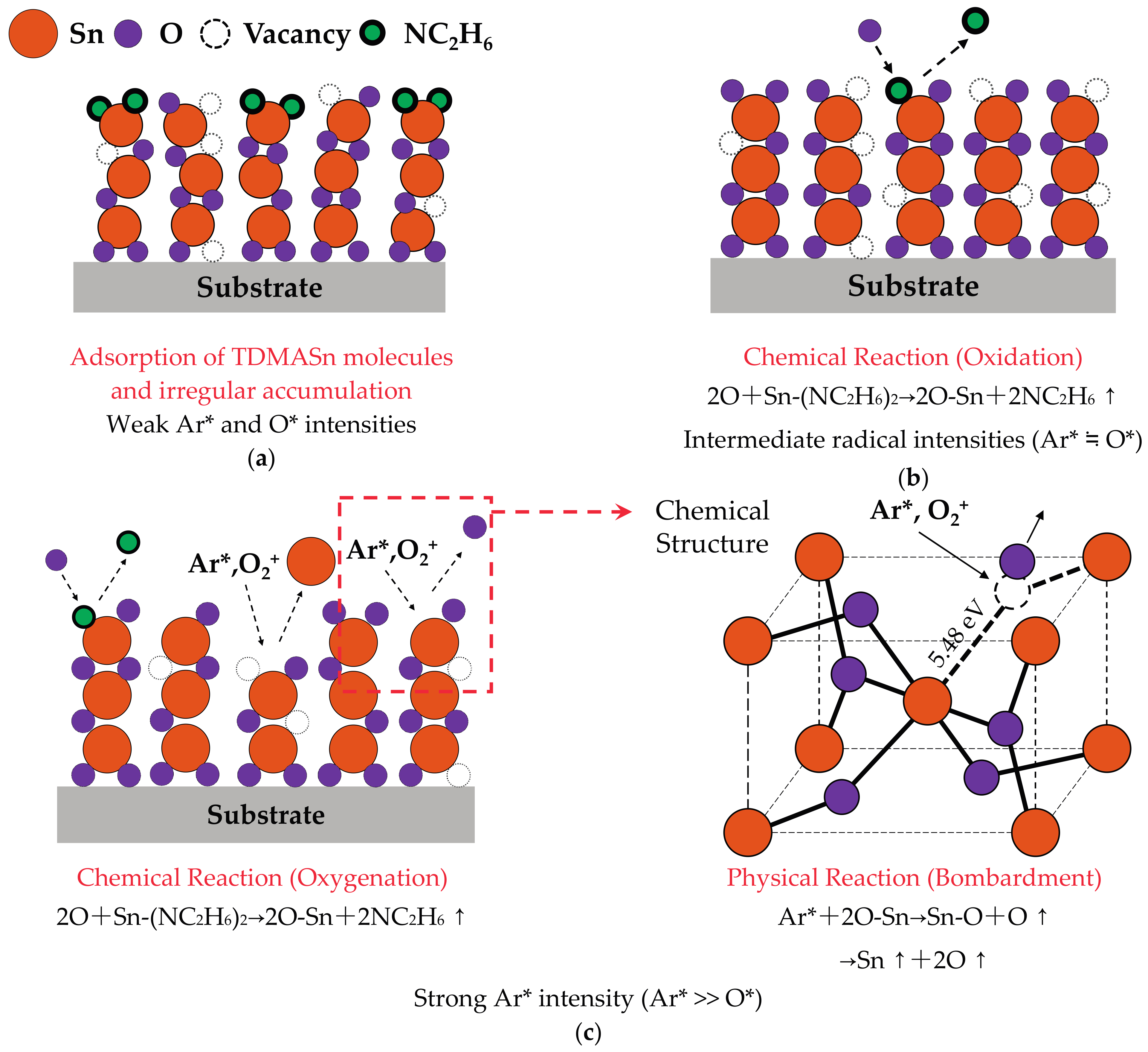
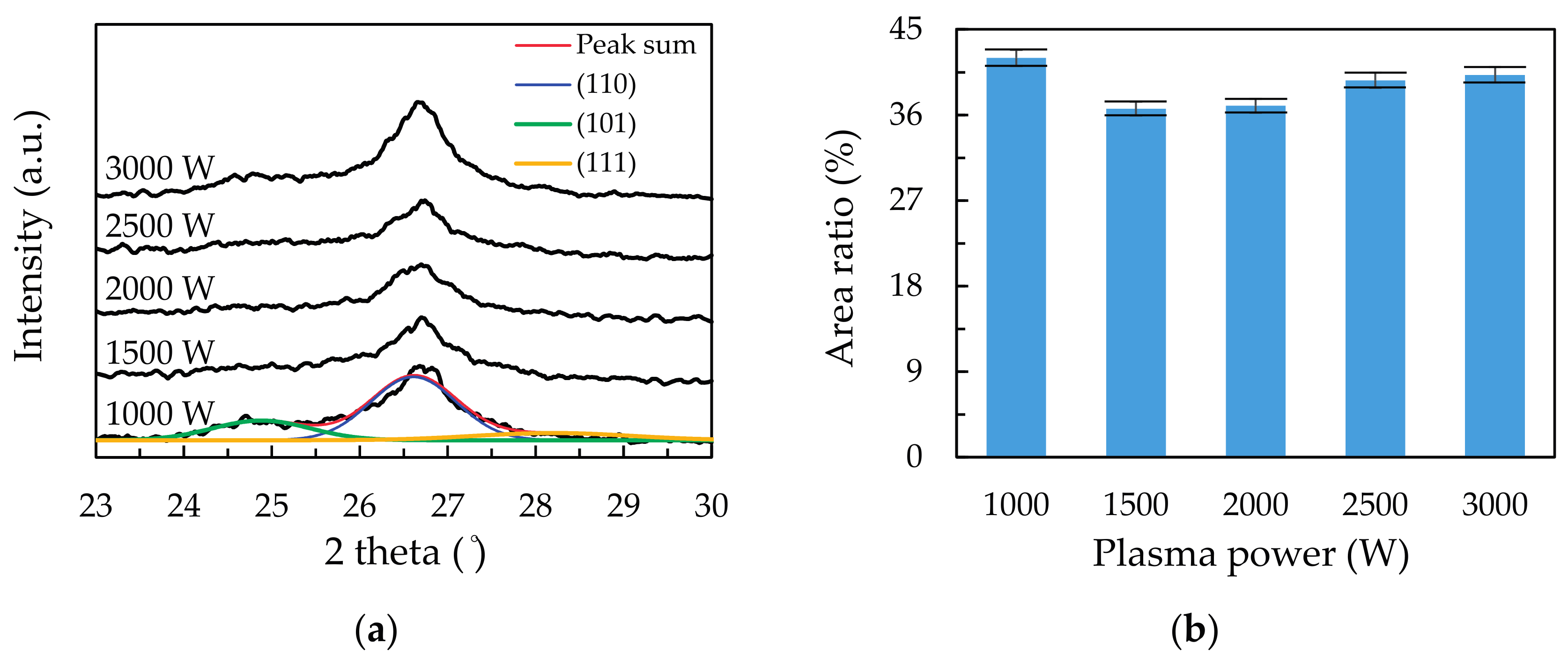
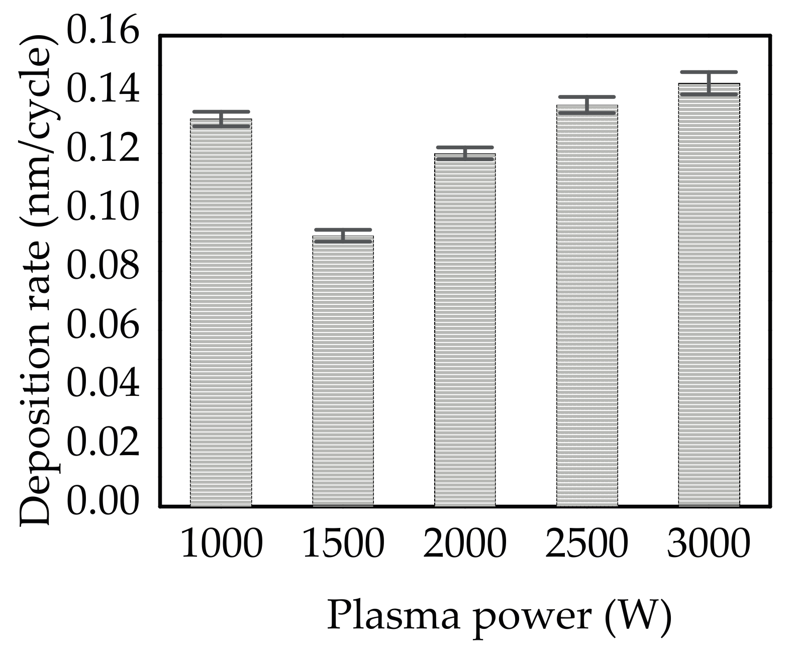
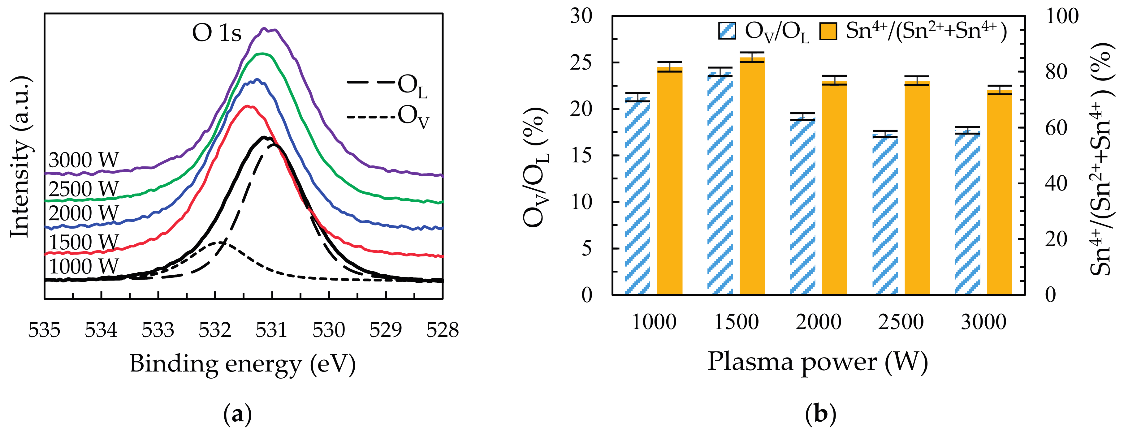
3.1. Deposition Mechanism

Figure 1a shows the intensity variation of ionized argon (Ar*) and oxygen (O*) at different plasma power by the OES measurement from 500 to 800 nm. The O peak (777 nm) is observed as the plasma power reaches 1500 W, revealing the dramatic increase of intensity. There is another O2+ peak at 526.8 nm from 500 to 600 nm obtained by 1000 W as shown in the inserted image of Figure 1a. Figure 1b indicates that the Ar* intensity increases continuously with the increased plasma power, contributing to the increase of O* amounts [31,35,36]. The O* intensity increases sharply from 1000 to 2000 W but remains unvarying afterwards. The power of 1000 W is too weak for electrons to obtain sufficient kinetic energy for collision with gas molecules, leading to the lower intensities of Ar* and O*. Therefore, the collision would increase with the rise of power, corresponding to the significantly increased intensities of Ar* and O* at 1500 and 2000 W. This result also shows that the degree of O2 ionization reaches maximum at 2000 W. It is reported that the excited energy of the Ar is lower than the dissociation energy of the O2. [37]. Furthermore, the Ar also enhances the dissociation of the O2. The intensity of O* thus saturates earlier than that of Ar* at increasing plasma power. The photo of glow discharge from Ar* and O* is shown as inserted image of Figure 1b. Figure 1c shows the intensities variation of O2+ peak obtained at different plasma powers. The lowest OES intensity of O2+ peak is observed at 1500 W. The overall intensities of O2+ peak are weaker than Ar* but the O2+ peak may be considered as a factor of ion bombardment. Thus, the film at 1500 W has the smallest ion bombardment due to the minimal sum of Ar* and O2+ intensities. The scheme of PEALD reactor with remote plasma and optical collimator is indicated in Figure 1d.
Three types of deposition mechanisms of PEALD SnO2 thin films are demonstrated in Figure 2: (a) weak Ar* and O* intensities, (b) similarly intermediate radical intensities (Ar* ≒ O*), and (c) strong Ar* intensity (Ar* >> O*). As shown in Figure 2a, corresponding to the deposition at 1000 W, the weak radical intensities do not cause enough bond breaking of precursors and oxidation due to the lower plasma density [31,35,36]. This unsaturated reaction causes the adsorption of precursor molecules and the irregular accumulation of Sn and O atoms. The deposition is in oxygen-deficient condition leading to the growth of oxygen vacancy defects and the loose structure of films [36,38,39]. As shown in Figure 2b, corresponding to 1500 W, the oxidation reaction begins to saturate due to the sufficient intensities of Ar* and O*. At the same time, the deposited structure is denser than other samples owing to the sufficient O* participating the film growth [24,25,36]. The film density usually has a strong correlation with the n [23]. The plasma power of 1500 W shows the largest n, suggesting the highest film density compared to other plasma powers. The increased Ar* intensity at 2000 and 2500 W may lead to damage on the films surface (although it could be trivial at this stage), inducing the reduced crystal structure. In Figure 2c corresponding to 3000 W, the Ar* and O2+ peak contributes to the ion bombardment. The much greater Ar* intensity than O* causes serious bombardment and severe structural destruction with the dissociation of Sn-O bonds. This bond breaking occurs when the energy of Ar* is higher than 5.48 eV [40] as shown in the inset of Figure 2c. As a consequence, the induced ion bombardment by too high a power will cause the serious damage to the deposited films although the saturation oxidation reaction is obtained. The deterioration of the film properties due to the strong plasma bombardment can also be found in some researches via MSD [4], and laser-assisted [12] or plasma enhanced CVD [13].
The XRD measurements have been performed, and the dominant (110) peaks for the films deposited at different plasma power are shown in Figure 3a. It is seen that there are shoulders at the both sides of the (110) peaks, and thus the peaks are further split into three parts. The shoulder peaks at 24.8° and 28.1° correspond to triclinic (101) and (111) Sn3O4, respectively (JCPDS no. 16-0737) [41,42]. The area ratio of the [(101)+(111)] Sn3O4 peak to total as a function of plasma power is shown in Figure 3b. The ratio is the lowest at 1500 W and increases when further increasing the plasma power. This in turn means that at high plasma powers, the films have an increased Sn3O4 formation and the reduced SnO2 crystalline structure.
Figure 4 shows the deposition rate (RD) of PEALD SnO2 films as a function of plasma power. The thickness of samples is in the range from 27.6 to 39.6 nm. The RD is defined by the film growth thickness per cycle. With the increased plasma power, the RD emerges a V-shaped trend with the lowest value at 1500 W. The high RD of 1.32 Å/cycle at 1000 W is due to the adsorption of TDMA-Sn molecules and irregular stacking of Sn and O atoms [38,39]. The insufficient oxidation reaction may lead to non-ideal ALD process, where the chemical vapor deposition-like process may occur and lead to a high RD due to the island growth [43]. In the range of 1500 to 3000 W, the increased RD from 0.92 to 1.44 Å/cycle is due to the enhanced plasma density [31,35,36] resulting from the increased Ar* intensity and sufficient O*. However, the increase of RD slows down, owing to the Ar* bombardment. This result can be reflected on the variation of the OV/OL ratio as shown later. We have changed the substrate temperature, TDMA-Sn dosing time, and oxygen plasma pulse time for the SnO2 deposition. The RD tends to saturate at 0.145 nm/cycle. In the present study, the plasma powers of 2500 to 3000 W have the RD of 0.14 to 0.144 nm/cycle, suggesting that the reaction gradually closes to saturation at the plasma power larger than 2500 W as the difference in RD between 2500 and 3000 W is small (0.004 nm/cycle).
The high-resolution O 1s spectra are shown in Figure 5a for the SnO2 films deposited at different plasma power. The O 1s curves are deconvoluted into two components. The lower binding energy peak at ~531 eV is typically assigned to O2− on the SnO2 lattice site (OL), while the higher binding energy component at ~532 eV is attributed to the oxygen in the SnO2 matrix with OV [24,25,26]. The compositions of the films prepared at different plasma powers are listed in Table 1. In Figure 5b, the OV/OL ratio of films shows the opposite trend to RD. The enhanced OV/OL ratio from 1000 to 1500 W is ~3% (21.2 to 24.1%) due to the sufficient O* which is induced the more saturated reaction. In the range of 1500 to 3000 W, the OV/OL ratio decreases due to Ar* bombardment. It is noted that the O* intensity at 2500 and 3000 W is unchanged. As a result, the excess power at 2500 and 3000 W mainly focuses on Ar*, leading to severe bombardment and destruction of films. This result is similar to some studies with high power [4,12,13]. The ratio of Sn4+/(Sn2++Sn4+) is also revealed in the Figure 5b. The major Sn4+ and minor Sn2+ states of films are assigned to the bonding of the OL and OV, respectively. Thus, the Sn 3d core level spectra via XPS for SnO2 thin films deposited at different plasma power from 1000 to 3000 W with the deconvolution of sample at 1000 W are shown in the Figure S1.

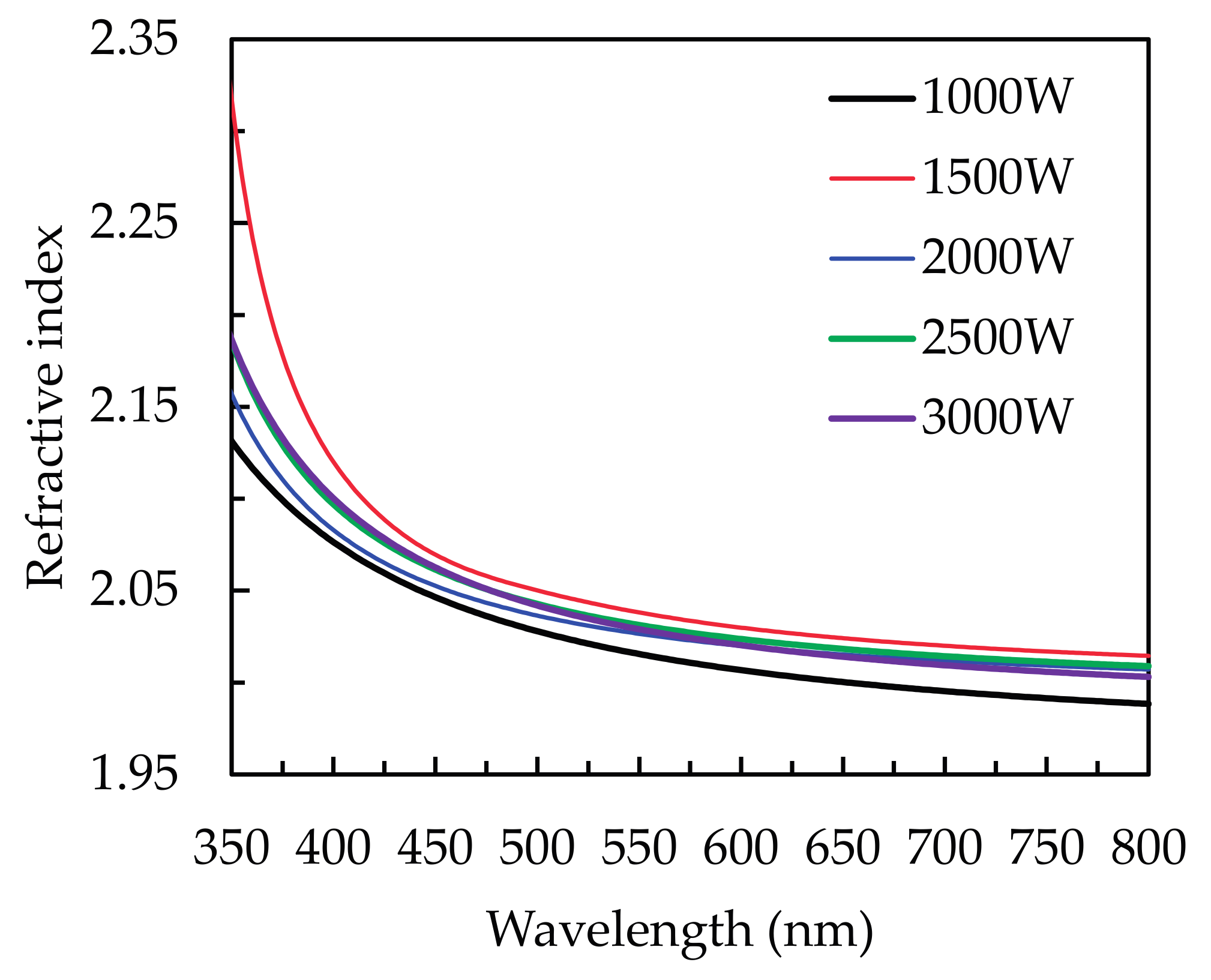
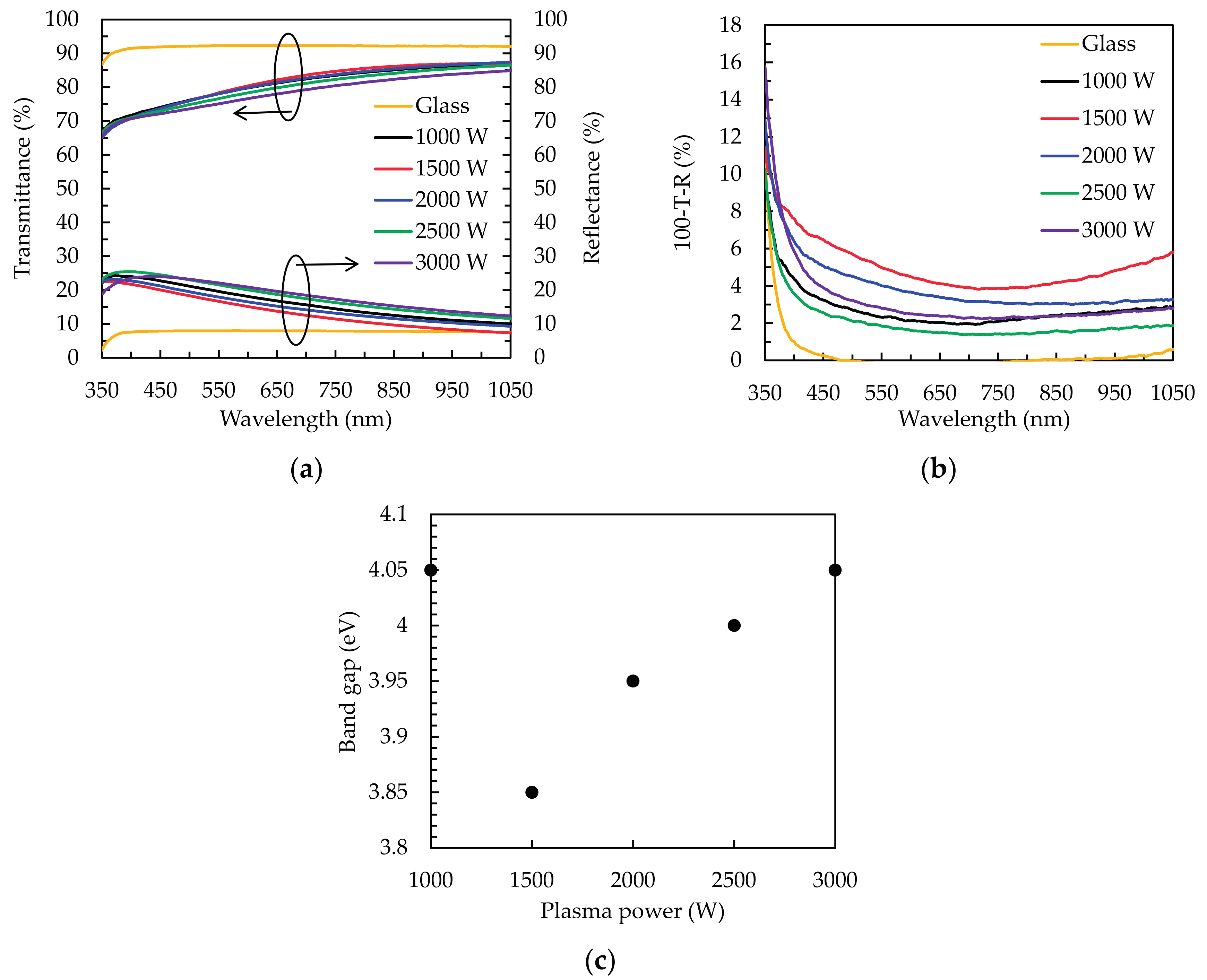
3.2. Optical Properties

The refractive indices (n) of all samples are shown as wavelength-dependent functions in Figure 6. The measured substrate is p-type (110) silicon wafers. The highest and lowest n values are at the plasma power is 1500 and 1000 W, respectively. The variation of n generally has strong correlations to the change of films density [23]. The lowest n at l000 W results from the poor film density obtained by the irregular accumulation of Sn and O atoms. The optimized n at l500 W is due to the densest structure, attributed to the saturated reaction by sufficient Ar* and O*. Thus, it is comprehensible that the decreased n at higher power than 1500 W is caused by bombardment of Ar* [23]. Compared to the literature using MSD [2,3], sol–gel [10], CVD [44], and thermal ALD [19,20,21], PEALD possess a great ability to deposit high-quality SnO2 thin films. The refractive indices of SnO2 thin films prepared by MSD, thermal evaporation and sol–gel process are 1.96, 2.12, and 2.07, respectively, at the wavelength of around 600 nm [4,5,10]. These values are similar to the values in the present study.
Figure 7a shows the transmittance and reflectance spectra of the SnO2 thin films deposited on the glass substrate at different plasma power. The sample of 1500 W exhibits the highest transmittance of ~80.9% and the lowest reflectance of ~14.3%. Furthermore, the variation of transmittance spectra reveals an inverse correlation to that of reflectance spectra. This change of transmittance spectra is mainly attributed to the reflection conditions caused by different n. Particular, at the short wavelength around 400 nm, only the reflectance changes and its trend reveals the red-shift phenomenon after 1500 W. The reason is attributed to the variation of n. The optical loss spectrum has estimated via the calculation of 100-T-R as shown in Figure 7b. The trend of optical loss illustrates the highest and lowest values of ~5% (1500 W) and ~2% (1000 W), respectively. This result is attributed to the consequences of light scattering induced by OV defects [45]. Another possible reason is that the slight absorption of free carriers in OV defects, leading to the narrowing of band gap (Eg) [46,47]. The Eg of the SnO2 thin films is determined by Tauc’s plots using the following equation:
αhν = A(hν − Eg)1/n,
where α is the absorption coefficient, hν is the energy of incident light, and A is the proportionality constant [23,26]. The value of exponent n is 2 for direct band gap materials, respectively. Figure 7c shows the dependence of the Eg on the plasma power. The evaluated Eg of the samples varies from 3.8 to 4.1 eV with the V-shaped trend, being the contrary variation of OV/OL ratio. The minimum value of Eg thus occurs at 1500 W. In addition, the unique distinction for the narrowest Eg at 1500 W is probably owing to the introduction of doping shallow energy level of OV under the conduction band [48]. We have measured OES spectra for the plasma powers of 1430, 1440, and 1450 W to estimate the minimum value of Eg. It is found that the intensities of Ar* and O* at 1430 and 1440 W are weak (similar to that at 1000 W), while the OES spectrum at 1450 W shows the dramatically increased O* intensities as similar to the case of 1500 W. The Eg of sample at 1450 W is measured as 3.86 eV, which is similar to that of 1500 W. For the power higher than 1500 W, the increase of Eg is due to the decrease of OV and optical loss. On the other hand, the d of sample is 52.7, 36.8, 48, 54.6, and 57.5 nm with a total of 400 PEALD cycles for the plasma power of 1000, 1500, 2000, 2500, and 3000 W, respectively. The relationship between the d and transmittance (T) is given by T = exp(−αd). The reflectance is known to be influenced by both of the d and n. The optical loss is thus also affected by the d. The highest optical loss of the thinnest film at 1500 W indicates a high α.

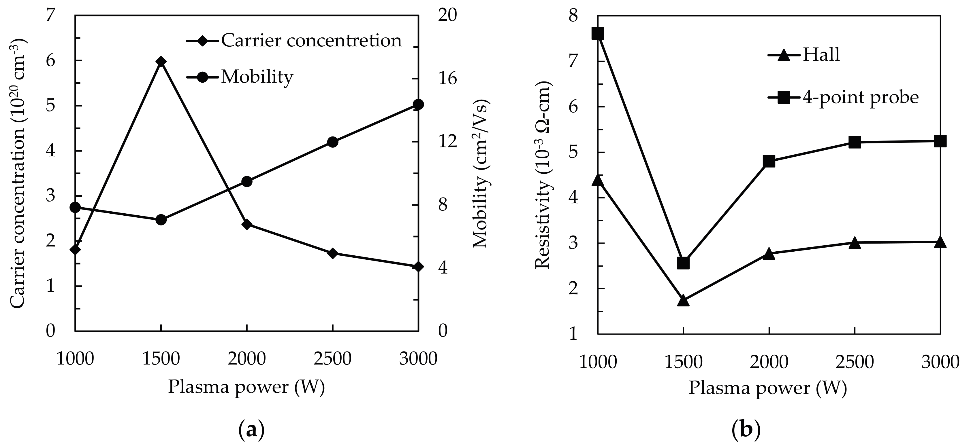
3.3. Electrical Properties

Figure 8a shows the measurements of carrier concentration (Ne) and mobility (µ) for SnO2 thin films on a glass substrate with the increased plasma power. We observe n-type conductivity for all films. The Ne curve sharply increases from 1000 to 1500 W, but dramatically drops from 1500 to 2000 W and then gently decreases. Similar trends have been investigated by some researches [22,24,25]. The increased Ne at 1500 W may be ascribed to the increased OV/OL ratio as oxygen vacancies have been evidenced as one of the main origins of Ne. The subsequent decrease in Ne should be related to the suppression of OV. As we know, the OV can be acted as the donor doping in metal oxide to the maintaining of charge neutrality. On the contrary, the µ shows an upward trend with the increased plasma power. The slight decrease of µ at 1500 W is 7.06 cm2/Vs with the highest Ne of 5.98 × 1020 cm3. This result can be attributed to the carrier scattering, leading to the inverse relationship between Ne and µ. As a result, the resistivity (ρ) measured by Hall effects and 4-point probe methods indicates an opposite trend with Ne as shown in Figure 8b. Lowest ρ values of 2.56 × 10⁻³ (4-point probe) and 1.48 × 10⁻³ Ω-cm (Hall-effect) at 1500 W. Then, ρ increases from 1500 to 2000 W and shows minor change in the range from 2000 to 3000 W owing to the reduction of OV defects, resulting from the bombardment of Ar*.

4. Conclusions

In this paper, the SnO2 thin films with high-quality are prepared by PEALD with Ar/O2 mixture gas as reactants at different plasma power from 1000 to 3000 W. The radical intensity obtained by OES mainly affects the bond breaking of precursors and the arrangement of Sn and O atoms, suggesting that the Ar* intensity increases with increasing plasma power to induce the increase of O* intensity and even the Ar* bombardment. The immutable change of O* intensity from 1500 W to 3000 W confirms not only the decreased OV/OL ratio from the highest 24.1 to 17.1%, but also the decreased films density by Ar* bombardment. The optimized n (higher than 2) with better transmittance and reflectance is obtained at 1500 W. The adsorption of precursor molecules and irregular accumulation resulting from insufficient radical intensity of Ar* and O* are the main reason for the higher RD of 1.32 Å/cycle at 1000 W. Despite the higher value of 4.05 eV is owing to the quantum size effects at 1000 W, the results of band gap also match the variation of optical loss curves due to the light scattering from OV defects. Besides, the power at 1500 W has the lowest ρ of 1.48 × 10⁻³ Ω-cm due to the highest Ne of 5.98 × 1020 cm3 and lowest ρ of 1.48 × 10⁻³ Ω-cm. The deposition mechanisms and the relationship between the plasma radicals and film properties presented in this study are expected to be helpful for the deposition of high-quality PEALD SnO2 films with excellent photoelectrical properties.

Supplementary Materials

The following are available online at https://www.mdpi.com/1996-1944/14/3/690/s1, Figure S1: The Sn 3d core level spectra via X-ray photoelectron spectroscopy (XPS) for SnO2 thin films deposited at different plasma power from 1000 to 3000 W with the deconvolution of sample at 1000 W.

Author Contributions

Conceptualization, S.-Y.L. and P.-H.H.; methodology, Z.-X.Z.; formal analysis, P.-H.H., Z.-X.Z., C.-H.H., W.-Y.W., C.-J.H., and S.-Y.L.; investigation, S.-Y.L. and P.-H.H. and Z.-X.Z.; writing—original draft preparation, P.-H.H. and Z.-X.Z.; writing—review and editing, S.-Y.L. and P.-H.H.; funding acquisition, S.-Y.L., P.-H.H., and C.-H.H. All authors have read and agreed to the published version of the manuscript.

Funding

This research was funded by the Natural Science Foundation of Fujian Province, grant numbers 2020J05151 and 2020H0025; the Education Department of Fujian Province, grant number JAT190300; the Scientific Research Projects of Jimei University, grant number ZQ2019032; the Scientific Research Projects of Xiamen University of Technology, grant numbers 405011904, 40199029, YKJ19001R, XPDKQ19006, HK-HX210106, and HK-HX201243; the Science and Technology Project in Xiamen, grant number 3502ZCQ20191002.

Data Availability Statement

Data sharing is not applicable to this article.

Acknowledgments

We appreciate the effort from Hsiu-Ling Huang to the administrative and technical support.

Conflicts of Interest

The authors declare no conflict of interest.

References

  1. Lim, D.; Jeon, Y.; Kim, M.; Kim, Y.; Kim, S. Electrical Characteristics of SnO2 Thin-Film Transistors Fabricated on Bendable Substrates Using Reactive Magnetron Sputtering. J. Nanosci. Nanotechnol. 2016, 16, 11697–11700. [Google Scholar] [CrossRef]
  2. Sun, W.; Wang, S.; Li, S.; Miao, X.; Zhu, Y.; Du, C.; Ma, R.; Wang, C. Reactive-Sputtered Prepared Tin Oxide Thin Film as an Electron Transport Layer for Planar Perovskite Solar Cells. Coatings 2019, 9, 320. [Google Scholar] [CrossRef] [Green Version]
  3. Qiu, L.; Liu, Z.; Ono, L.K.; Jiang, Y.; Son, D.; Hawash, Z.; He, S.; Qi, Y. Scalable Fabrication of Stable High Efficiency Perovskite Solar Cells and Modules Utilizing Room Temperature Sputtered SnO2 Electron Transport Layer. Adv. Funct. Mater. 2019, 29, 1806779. [Google Scholar] [CrossRef] [Green Version]
  4. Shanker, G.; Prathap, P.; Srivatsa, K.M.K.; Singh, P. Effect of Balanced and Unbalanced Magnetron Sputtering Processes on the Properties of SnO2 Thin Films. Curr. Appl. Phys. 2019, 19, 697–703. [Google Scholar] [CrossRef]
  5. Howari, H.; Tomsah, I.B.I. Structural, Optical and Ellipsometric Characteristics of PVD Synthesized SnO2 Thin Films on Pt Coated Silicon Wafers. Optik 2017, 144, 467–474. [Google Scholar] [CrossRef]
  6. Iizuka, K.; Kambara, M.; Yoshida, T. Highly Sensitive SnO2 Porous Film Gas Sensors Fabricated by Plasma Spray Physical Vapor Deposition. Sens. Actuators B Chem. 2012, 173, 455–461. [Google Scholar] [CrossRef]
  7. Korotcenkov, G.; Cho, B.K. Spray Pyrolysis Deposition of Undoped SnO2 and In2O3 Films and Their Structural Properties. Prog. Cryst. Growth Charact. Mater. 2017, 63, 1–47. [Google Scholar] [CrossRef]
  8. Köse, H.; Karaal, Ş.; Aydin, A.O.; Akbulut, H. Structural Properties of Size-Controlled SnO2 Nanopowders Produced by Sol–Gel Method. Mater. Sci. Semicond. Process. 2015, 38, 404–412. [Google Scholar] [CrossRef]
  9. Kumar, V.; Swart, H.C.; Gohain, M.; Bezuidenhoudt, B.C.B.; van Vuuren, A.J.; Lee, M.; Ntwaeaborwa, O.M. The Role of Neutral and Ionized Oxygen Defects in the Emission of Tin Oxide Nanocrystals for near White Light Application. Nanotechnology 2015, 26, 295703. [Google Scholar] [CrossRef]
  10. Wang, J.; Ge, J.; Hou, H.; Wang, M.; Liu, G.; Qiao, G.; Wang, Y. Design and Sol–Gel Preparation of SiO2/TiO2 and SiO2/SnO2/SiO2–SnO2 Multilayer Antireflective Coatings. Appl. Surf. Sci. 2017, 422, 970–974. [Google Scholar] [CrossRef]
  11. Kassem, O.; Saadaoui, M.; Rieu, M.; Viricelle, J.-P. A Novel Approach to a Fully Inkjet Printed SnO 2 -Based Gas Sensor on a Flexible Foil. J. Mater. Chem. C 2019, 7, 12343–12353. [Google Scholar] [CrossRef]
  12. Kwoka, M.; Ottaviano, L.; Waczyńska, N.; Santucci, S.; Szuber, J. Influence of Si Substrate Preparation on Surface Chemistry and Morphology of L-CVD SnO2 Thin Films Studied by XPS and AFM. Appl. Surf. Sci. 2010, 256, 5771–5775. [Google Scholar] [CrossRef]
  13. Pan, J.; Ganesan, R.; Shen, H.; Mathur, S. Plasma-Modified SnO2 Nanowires for Enhanced Gas Sensing. J. Phys. Chem. C 2010, 114, 8245–8250. [Google Scholar] [CrossRef]
  14. Lu, Y.M.; Jiang, J.; Becker, M.; Kramm, B.; Chen, L.; Polity, A.; He, Y.B.; Klar, P.J.; Meyer, B.K. Polycrystalline SnO2 Films Grown by Chemical Vapor Deposition on Quartz Glass. Vacuum 2015, 122, 347–352. [Google Scholar] [CrossRef]
  15. Verchère, A.; Mishra, S.; Jeanneau, E.; Guillon, H.; Decams, J.-M.; Daniele, S. Heteroleptic Tin(IV) Aminoalkoxides and Aminofluoroalkoxides as MOCVD Precursors for Undoped and F-Doped SnO2 Thin Films. Inorg. Chem. 2020, 59, 7167–7180. [Google Scholar] [CrossRef] [PubMed]
  16. Zhu, L.-Y.; Yuan, K.; Yang, J.-G.; Ma, H.-P.; Wang, T.; Ji, X.-M.; Feng, J.-J.; Devi, A.; Lu, H.-L. Fabrication of Heterostructured P-CuO/n-SnO2 Core-Shell Nanowires for Enhanced Sensitive and Selective Formaldehyde Detection. Sens. Actuators B Chem. 2019, 290, 233–241. [Google Scholar] [CrossRef]
  17. Ahmed, B.; Anjum, D.H.; Gogotsi, Y.; Alshareef, H.N. Atomic Layer Deposition of SnO 2 on MXene for Li-Ion Battery Anodes. Nano Energy 2017, 34, 249–256. [Google Scholar] [CrossRef] [Green Version]
  18. Park, H.; Choi, H.; Lee, N.; Jung, C.; Choi, Y.; Song, S.; Choi, Y.; Kim, K.; Kim, J.; Lee, J.; et al. Effect of Single Al2O3 Cycle Insertion with Various Positions in SnO2 Thin Films Using Atomic Layer Deposition. Ceram. Int. 2020, 46, 12782–12787. [Google Scholar] [CrossRef]
  19. Jeong, S.; Seo, S.; Park, H.; Shin, H. Atomic Layer Deposition of a SnO2 Electron-Transporting Layer for Planar Perovskite Solar Cells with a Power Conversion Efficiency of 18.3%. Chem. Commun. 2019, 55, 2433–2436. [Google Scholar] [CrossRef]
  20. Su, L.; Zuo, Y.; Xie, J. Scalable Manufacture of Vertical p-GaN/n-SnO2 Heterostructure for Self-powered Ultraviolet Photodetector, Solar Cell and Dual-color Light Emitting Diode. InfoMat 2020, inf2.12127. [Google Scholar] [CrossRef]
  21. Choi, D.; Maeng, W.J.; Park, J.-S. The Conducting Tin Oxide Thin Films Deposited via Atomic Layer Deposition Using Tetrakis-Dimethylamino Tin and Peroxide for Transparent Flexible Electronics. Appl. Surf. Sci. 2014, 313, 585–590. [Google Scholar] [CrossRef]
  22. Lee, B.K.; Jung, E.; Kim, S.H.; Moon, D.C.; Lee, S.S.; Park, B.K.; Hwang, J.H.; Chung, T.-M.; Kim, C.G.; An, K.-S. Physical/Chemical Properties of Tin Oxide Thin Film Transistors Prepared Using Plasma-Enhanced Atomic Layer Deposition. Mater. Res. Bull. 2012, 47, 3052–3055. [Google Scholar] [CrossRef]
  23. Kuang, Y.; Zardetto, V.; van Gils, R.; Karwal, S.; Koushik, D.; Verheijen, M.A.; Black, L.E.; Weijtens, C.; Veenstra, S.; Andriessen, R.; et al. Low-Temperature Plasma-Assisted Atomic-Layer-Deposited SnO2 as an Electron Transport Layer in Planar Perovskite Solar Cells. Acs Appl. Mater. Interfaces 2018, 10, 30367–30378. [Google Scholar] [CrossRef] [PubMed]
  24. Chistiakova, G.; Mews, M.; Wilks, R.G.; Bär, M.; Korte, L. In-System Photoelectron Spectroscopy Study of Tin Oxide Layers Produced from Tetrakis(Dimethylamino)Tin by Plasma Enhanced Atomic Layer Deposition. J. Vac. Sci. Technol. A Vac. Surf. Film. 2018, 36, 02D401. [Google Scholar] [CrossRef]
  25. Kim, H.Y.; Nam, J.H.; George, S.M.; Park, J.-S.; Park, B.K.; Kim, G.H.; Jeon, D.J.; Chung, T.-M.; Han, J.H. Phase-Controlled SnO2 and SnO Growth by Atomic Layer Deposition Using Bis(N-Ethoxy-2,2-Dimethyl Propanamido)Tin Precursor. Ceram. Int. 2019, 45, 5124–5132. [Google Scholar] [CrossRef]
  26. Mai, L.; Zanders, D.; Subaşı, E.; Ciftyurek, E.; Hoppe, C.; Rogalla, D.; Gilbert, W.; de los Arcos, T.; Schierbaum, K.; Grundmeier, G.; et al. Low-Temperature Plasma-Enhanced Atomic Layer Deposition of Tin(IV) Oxide from a Functionalized Alkyl Precursor: Fabrication and Evaluation of SnO2-Based Thin-Film Transistor Devices. ACS Appl. Mater. Interfaces 2019, 11, 3169–3180. [Google Scholar] [CrossRef]
  27. Profijt, H.B.; Potts, S.E.; van de Sanden, M.C.M.; Kessels, W.M.M. Plasma-Assisted Atomic Layer Deposition: Basics, Opportunities, and Challenges. J. Vac. Sci. Technol. A Vac. Surf. Film. 2011, 29, 050801. [Google Scholar] [CrossRef] [Green Version]
  28. Yang, Y.; Wang, Y.; Yin, S. Oxygen Vacancies Confined in SnO2 Nanoparticles for Desirable Electronic Structure and Enhanced Visible Light Photocatalytic Activity. Appl. Surf. Sci. 2017, 420, 399–406. [Google Scholar] [CrossRef]
  29. Ma, D.; Li, Y.; Zhang, P.; Lin, Z. Oxygen Vacancy Engineering in Tin(IV) Oxide Based Anode Materials toward Advanced Sodium-Ion Batteries. ChemSusChem 2018, 11, 3693–3703. [Google Scholar] [CrossRef]
  30. Ilka, M.; Bera, S.; Kwon, S.-H. Influence of Surface Defects and Size on Photochemical Properties of SnO2 Nanoparticles. Materials 2018, 11, 904. [Google Scholar] [CrossRef] [Green Version]
  31. Lee, C.; Lieberman, M.A. Global Model of Ar, O2, Cl2, and Ar/O2 High-density Plasma Discharges. J. Vac. Sci. Technol. A Vac. Surf. Film. 1995, 13, 368–380. [Google Scholar] [CrossRef]
  32. Hsu, C.-H.; Cho, Y.-S.; Liu, T.-X.; Chang, H.-W.; Lien, S.-Y. Optimization of Residual Stress of SiO2/Organic Silicon Stacked Layer Prepared Using Inductively Coupled Plasma Deposition. Surf. Coat. Technol. 2017, 320, 293–297. [Google Scholar] [CrossRef]
  33. Lien, S.-Y.; Cho, Y.-S.; Hsu, C.-H.; Shen, K.-Y.; Zhang, S.; Wu, W.-Y. Mechanism of Dense Silicon Dioxide Films Deposited under 100 °C via Inductively Coupled Plasma Chemical Vapor Deposition. Surf. Coat. Technol. 2019, 359, 247–251. [Google Scholar] [CrossRef]
  34. Mackus, A.J.M.; Heil, S.B.S.; Langereis, E.; Knoops, H.C.M.; van de Sanden, M.C.M.; Kessels, W.M.M. Optical Emission Spectroscopy as a Tool for Studying, Optimizing, and Monitoring Plasma-Assisted Atomic Layer Deposition Processes. J. Vac. Sci. Technol. A Vac. Surf. Film. 2010, 28, 77–87. [Google Scholar] [CrossRef] [Green Version]
  35. Takamatsu, T.; Uehara, K.; Sasaki, Y.; Miyahara, H.; Matsumura, Y.; Iwasawa, A.; Ito, N.; Azuma, T.; Kohno, M.; Okino, A. Investigation of Reactive Species Using Various Gas Plasmas. RSC Adv. 2014, 4, 39901–39905. [Google Scholar] [CrossRef] [Green Version]
  36. Takechi, K.; Lieberman, M.A. Effect of Ar Addition to an O2 Plasma in an Inductively Coupled, Traveling Wave Driven, Large Area Plasma Source: O2/Ar Mixture Plasma Modeling and Photoresist Etching. J. Appl. Phys. 2001, 90, 3205–3211. [Google Scholar] [CrossRef]
  37. Berenguer, C.; Katsonis, K. Plasma Reactors and Plasma Thrusters Modeling by Ar Complete Global Models. Int. J. Aerosp. Eng. 2012, 2012, 1–18. [Google Scholar] [CrossRef]
  38. Marichy, C.; Donato, N.; Willinger, M.-G.; Latino, M.; Karpinsky, D.; Yu, S.-H.; Neri, G.; Pinna, N. Tin Dioxide Sensing Layer Grown on Tubular Nanostructures by a Non-Aqueous Atomic Layer Deposition Process. Adv. Funct. Mater. 2011, 21, 658–666. [Google Scholar] [CrossRef]
  39. Lim, S.-S. Atomic Layer Deposition of SnO2 Thin Films Using Tetraethyltin and H2O2. Ceram. Int. 2019, 6, 20600–20605. [Google Scholar] [CrossRef]
  40. Dean, J.A. (Ed.) Lange’s Handbook of Chemistry, 14th ed.; McGraw-Hill: New York, NY, USA, 1992; ISBN 978-0-07-016194-8. [Google Scholar]
  41. White, T.A.; Moreno, M.S.; Midgley, P.A. Structure Determination of the Intermediate Tin Oxide Sn3O4 by Precession Electron Diffraction. Z. Für Krist. 2010, 225. [Google Scholar] [CrossRef] [Green Version]
  42. Wu, J.; Xie, Y.; Du, S.; Ren, Z.; Yu, P.; Wang, X.; Wang, G.; Fu, H. Heterophase Engineering of SnO2/Sn3O4 Drives Enhanced Carbon Dioxide Electrocatalytic Reduction to Formic Acid. Sci. China Mater. 2020, 63, 2314–2324. [Google Scholar] [CrossRef]
  43. Richey, N.E.; de Paula, C.; Bent, S.F. Understanding Chemical and Physical Mechanisms in Atomic Layer Deposition. J. Chem. Phys. 2020, 152, 040902. [Google Scholar] [CrossRef] [PubMed]
  44. Outemzabet, R.; Doulache, M.; Trari, M. Physical and Photoelectrochemical Properties of Sb-Doped SnO2 Thin Films Deposited by Chemical Vapor Deposition: Application to Chromate Reduction under Solar Light. Appl. Phys. A 2015, 119, 589–596. [Google Scholar] [CrossRef]
  45. Koo, B.-R.; Bae, J.-W.; Ahn, H.-J. Optoelectronic Multifunctionality of Combustion-Activated Fluorine-Doped Tin Oxide Films with High Optical Transparency. Ceram. Int. 2019, 45, 10260–10268. [Google Scholar] [CrossRef]
  46. Peelaers, H.; Kioupakis, E.; Van de Walle, C.G. Fundamental Limits on Optical Transparency of Transparent Conducting Oxides: Free-Carrier Absorption in SnO2. Appl. Phys. Lett. 2012, 100, 011914. [Google Scholar] [CrossRef] [Green Version]
  47. Peelaers, H.; Kioupakis, E.; Van de Walle, C.G. Free-Carrier Absorption in Transparent Conducting Oxides: Phonon and Impurity Scattering in SnO2. Phys. Rev. B 2015, 92, 235201. [Google Scholar] [CrossRef] [Green Version]
  48. Norek, M.; Putkonen, M.; Zaleszczyk, W.; Budner, B.; Bojar, Z. Morphological, Structural and Optical Characterization of SnO2 Nanotube Arrays Fabricated Using Anodic Alumina (AAO) Template-Assisted Atomic Layer Deposition. Mater. Charact. 2018, 136, 52–59. [Google Scholar] [CrossRef]
Figure 1. (a) Optical emission spectroscopy (OES) spectra, and (b) intensity variation of O*, Ar*, and (c) O2+ with increased power from 1000 to 3000 W in plasma-enhanced atomic layer deposition (PEALD) SnO2 thin films deposition. The inserted image is the photo of glow discharge at 1500 W. (d) The schematic diagram for the ionization of Ar and O2 gas in PEALD process equipped with the OES optical collimator.
Materials 14 00690 g001aMaterials 14 00690 g001b
Figure 2. Deposition mechanisms of PEALD SnO2 thin films under three kinds of Ar* and O* intensities: (a) weak, (b) similarly intermediate (Ar* ≒ O*), and (c) strong (Ar* >> O*). The inserted image is the chemical structure diagram of films via Ar* and O2+ bombardment.
Materials 14 00690 g002
Figure 3. (a) Deconvolution of the (110) peak from X-ray diffraction (XRD) patterns for the 2-theta range of 23 to 30°. (b) Area ratio of the [(101) + (111)]/total as a function of plasma power.
Materials 14 00690 g003
Figure 4. Deposition rate (RD) of PEALD SnO2 thin films deposited at different plasma power from 1000 to 3000 W.
Materials 14 00690 g004
Figure 5. (a) The O 1s core level spectra via X-ray photoelectron spectroscopy (XPS) for SnO2 thin films deposited at different plasma power from 1000 to 3000 W with the deconvolution of sample at 1000 W and the (b) ratio of oxygen vacancies (OV) to lattice oxygen (OL) and the Sn4+/(Sn2+ + Sn4+).
Materials 14 00690 g005
Figure 6. The wavelength-dependent refractive index (n) of the PEALD SnO2 thin films deposited at different plasma power from 1000 to 3000 W.
Materials 14 00690 g006
Figure 7. (a) Transmittance and reflectance spectra, (b) optical loss spectra, and (c) band gap (Eg) of the PEALD SnO2 thin films obtained by different plasma power.
Materials 14 00690 g007
Figure 8. The (a) variation of carrier concentration (Ne) and mobility (µ) and (b) the results of resistivity (ρ) via respective hall and 4-point probe measurement for the SnO2 thin films with the increased plasma power from 1000 to 3000 W.
Materials 14 00690 g008
Table 1. Elemental composition of SnO2 thin films prepared at different plasma power.
Plasma Power
(W)
CompositionAtomic Ratio [O/Sn]
O
(%)
Sn
(%)
100064.235.81.79
150064.235.81.79
200064.135.91.79
250064.036.01.78
300064.235.81.79
Publisher’s Note: MDPI stays neutral with regard to jurisdictional claims in published maps and institutional affiliations.

