Article

Deposition, Characterization, and Modeling of Scandium-Doped Aluminum Nitride Thin Film for Piezoelectric Devices

1
Shanghai Normal University, Shanghai 200234, China
2
Department of Electrical and Electronic Engineering, Lee Kong Chian Faculty of Engineering and Science, Universiti Tunku Abdul Rahman, Kajang 43000, Malaysia
3
Department of Physics, University of Malaya, Kuala Lumpur 50603, Malaysia
4
State Key Laboratory of Luminescence and Applications, Changchun Institute of Optics, Mechanics and Physics, Chinese Academy of Sciences, Changchun 130033, China
*
Authors to whom correspondence should be addressed.
Materials 2021, 14(21), 6437; https://doi.org/10.3390/ma14216437
Submission received: 23 September 2021 / Revised: 14 October 2021 / Accepted: 20 October 2021 / Published: 27 October 2021
(This article belongs to the Special Issue Advanced Piezoelectric Materials: Science and Technology)

Abstract

:
In this work, we systematically studied the deposition, characterization, and crystal structure modeling of ScAlN thin film. Measurements of the piezoelectric device’s relevant material properties, such as crystal structure, crystallographic orientation, and piezoelectric response, were performed to characterize the Sc0.29Al0.71N thin film grown using pulsed DC magnetron sputtering. Crystal structure modeling of the ScAlN thin film is proposed and validated, and the structure–property relations are discussed. The investigation results indicated that the sputtered thin film using seed layer technique had a good crystalline quality and a clear grain boundary. In addition, the effective piezoelectric coefficient d33 was up to 12.6 pC/N, and there was no wurtzite-to-rocksalt phase transition under high pressure. These good features demonstrated that the sputtered ScAlN is promising for application in high-coupling piezoelectric devices with high-pressure stability.

1. Introduction

Piezoelectric devices have received increasing interest in a variety of applications in advanced electronic and in-formation industries, where they are used as resonators, filters, sensors, and actuators [1,2,3,4,5]. The properties of those piezoelectric devices mainly depend on the choice of piezoelectric materials. Bulk crystal materials are the most commonly used, but piezoelectric thin films such as zinc oxide (ZnO) and aluminum nitride (AlN) are emerging alternatives. Recently, AlN has attracted much attention due to its outstanding features such as high thermal stability, high acoustic velocity, low acoustic loss, and in particular, good compatibility with the complementary metal–oxide–semiconductor (CMOS) manufacturing process, which is promising for integrated sensors/actuators on silicon substrates. As for piezoelectric device applications, piezoelectricity is the main possibility investigated to offer efficiency electromechanical coupling. However, the piezoelectric response of pure AlN thin film is relatively small (d33 ≈ 5.5 pC/N) [6], which results in a low electromechanical coupling coefficient (kt2 = 6~7%) [7], and thus limits its important applications in technology such as high-sensitivity micromachined medical ultrasonic devices and wideband wireless communication filters [8,9].
It is known that the IIIA nitrides are AlN, GaN, and InN, and that these nitrides have a wurtzite structure [10,11]. First-principle calculations have indicated that a ScN wurtzite structure and the fabrication of Sc-IIIA-N nitrides are possible [10,12], and researchers found that the piezoelectric response of hexagonal Sc-IIIA-N was enhanced [13,14,15]. To enhance the piezoelectricity of AlN, Akiyama et al. [6] first fabricated and investigated piezoelectric properties of scandium (Sc)-doped AlN; i.e., the ScxAl1−xN alloy. It was demonstrated that the ScxAl1−xN films with a Sc concentration of 43% exhibited a four times larger piezoelectric response than pure AlN films. Wingqvist et al. [7] validated that the electromechanical coupling coefficient kt2 of Sc0.3Al0.7N could be enhanced up to 15%, almost twice that of pure AlN (7%). During the last decades, ScxAl1−xN thin film layered piezoelectric structures achieving strong coupling have attracted increasing attention worldwide. The ScxAl1−xN thin-film-based resonators with high Sc concentration offer prospects for developing high-frequency and broad wideband acoustic wave filters for fifth-generation (5G) mobile communication [16,17,18]. Nevertheless, mass production of such ScAlN films (more than 20% Sc content) with good crystalline quality and excellent piezoelectric properties is still difficult, and thus gives rise to limitations in wide applications [19,20,21,22]. To deal with this problem, the crystal structure of ScxAl1-xN thin film is worthy of being explored in great detail. Previously, Akiyama et al. reported XRD patterns and lattice constants of ScxAl1−xN alloys at various different Sc concentrations [6]. Zukauskaite et al. presented TEM micrographs and corresponding SAED patterns of AlN, Sc0.2Al0.8N, and Sc0.3Al0.7N films, and studied the microstructure and crystal quality of the films [23]. Deng et al. reported Raman scattering spectra for a sapphire substrate and ScxAl1−xN layers with x = 0–0.16 [24]. However, these previous studies mainly focused on the influences of Sc concentration on piezoelectric properties, so there is still a lack of information from a systematic investigation. For example, there is no report on the structure properties of ScxAl1−xN alloy thin films under high pressure or a high electric field, and it is very important to disclose the coupling between elastic and electric properties and structure–property relations, especially for piezoelectric-susceptible materials.
Therefore, in this work, a ScAlN thin film was systematically investigated in terms of deposition, characterization, and crystal structure modeling. First, the Sc0.29Al0.71N thin film was deposited on a 6-inch Mo/SiO2/AlN/SOI substrate by employing a pulsed DC magnetron sputtering system. Then, measurements of the piezoelectric-device-relevant material properties, such as crystal structure, crystallographic orientation, and piezoelectric response, were performed to characterize the sputtered thin film. The crystal structure and lattice patterns of the sputtered thin film were investigated by high-resolution transmission electron microscopy. According to the analysis of the selected area electron diffraction pattern, the crystal structure of Sc0.29Al0.71N was hexagonal phase. First-principles calculations were also performed to study the structural and electronic properties of Sc0.29Al0.71N. The calculated lattice parameters were in good agreement with the measured results. The chemical bonding states of Sc-doped AlN were investigated by X-ray photoemission spectroscopy. In addition, high-pressure Raman spectroscopy was employed to study the evolution of vibrational frequencies of the ScAlN phonons. The investigation results indicated that the ScAlN thin film could maintain material properties under high pressure, which is very important to ensure stable and reliable device performance, especially for piezoelectric pressure sensors.

2. Experimental

2.1. Deposition of ScAlN Thin Film

In this work, a conventional pulsed DC magnetron sputtering system (Sigma fxP PVD system, SPTS) was employed for the ScAlN thin-film deposition. This PVD cluster system consisted of four process chambers (AlN chamber, AlScN chamber, Mo chamber, and preclean chamber) and one transport chamber. The AlScN sputtering chamber was equipped with a 12-inch Sc0.3-Al0.7 alloy target. The ScAlN film was deposited on 6-inch Mo/SiO2/AlN/SOI substrate without vacuum breaking. Table 1 shows the deposition conditions of the ScAlN deposition. For deposition, the SOI wafer was cleaned successively by high temperature degas and argon ion soft etching in the clean chamber to ensure clean surfaces for film growth, and a Mo (110) thin film was prepared as a bottom electrode for electrical property measurements. During the deposition, the substrate was rotated 90° four times to ensure film uniformity. It is worth mentioning that before sputtering the Mo layer, we used SiO2 and AlN as a seed layer to improve the quality of the ScAlN (002) with better crystal orientation.

2.2. Characterization of ScAlN Thin Film

Next, measurements of the piezoelectric-device-relevant material properties were performed to characterize the Sc0.29Al0.71N thin film grown using pulsed DC magnetron sputtering. A scanning electron microscope (SEM, S-4800, Hitachi, Chiyoda, Japan) was used to investigate the microstructure and obtain a cross-sectional view of the sputtered film, and the component analysis was performed with an energy dispersive spectroscope (EDS). Transmission electron microscopy (TEM, JEM-2100F, JEOL, Akishima, Japan) was used to characterize the microstructure at the nanometric level. The crystal orientations and piezoelectric properties of the Sc0.29Al0.71N thin films were characterized by high-resolution X-ray diffraction (HRXRD, D8 ADVANCE, BRUKER, Billerica, USA) and a ferroelectric analyzer (TF-2000, aixACCT, Aachen, Germany), respectively.
In order to investigate the pressure-induced phase transformations, in situ high-pressure Raman measurements (up to 20 GPa) were conducted in a symmetric diamond anvil cell (DAC) with a diamond culet size of 300 μm in diameter. A small piece of the Sc0.29Al0.71N sample with ~27 μm thickness on the Mo/SiO2/SOI substrate was loaded into a sample chamber 100 μm in diameter drilled in the center of a T301 stainless-steel gasket. Silicone oil was used as the pressure-transmitting medium, and the pressure calibration was done using ruby fluorescence. An argon ion laser (=532 nm) was used as the excitation source, and the diameter of the focused laser radiation area was 10 μm.

2.3. Crystal Structure Modeling of ScAlN Thin Film

As for modeling of crystal structure of the sputtered Sc0.29Al0.71N thin film, first-principles calculations based on density functional theory (DFT) were carried out using the Quantum ESPRESSO codes [25,26]. PBEsol functional was used within the generalized gradient approximation (GGA) [27]. We employed the PAW pseudopotential to describe the electron–ion interaction. The plane-waves kinetic energy and charge densities cutoff were set to 50 Ry and 402 Ry, respectively. All the calculations were carried out on a 5 × 5 × 5 Monkhorst–Pack grid. Structural relaxation was carried out until the residual force had converged to less than 0.0001 Ry/a.u.
The calculated crystal structure of the Sc0.29Al0.71N was verified by comparison of the lattice constant to the TEM measurement results at the micro-nanometric level. In addition, X-ray photoelectron spectra (XPS) was used to characterize the chemical bonds of the Sc-doped AlN thin film. The X-ray photoemission spectroscopy (XPS) measurements were carried out on a VG ESCALAB MKII spectrometer (VG Scientific Ltd., London, UK) using a monochromatic Al X-ray beam

3. Results and Discussion

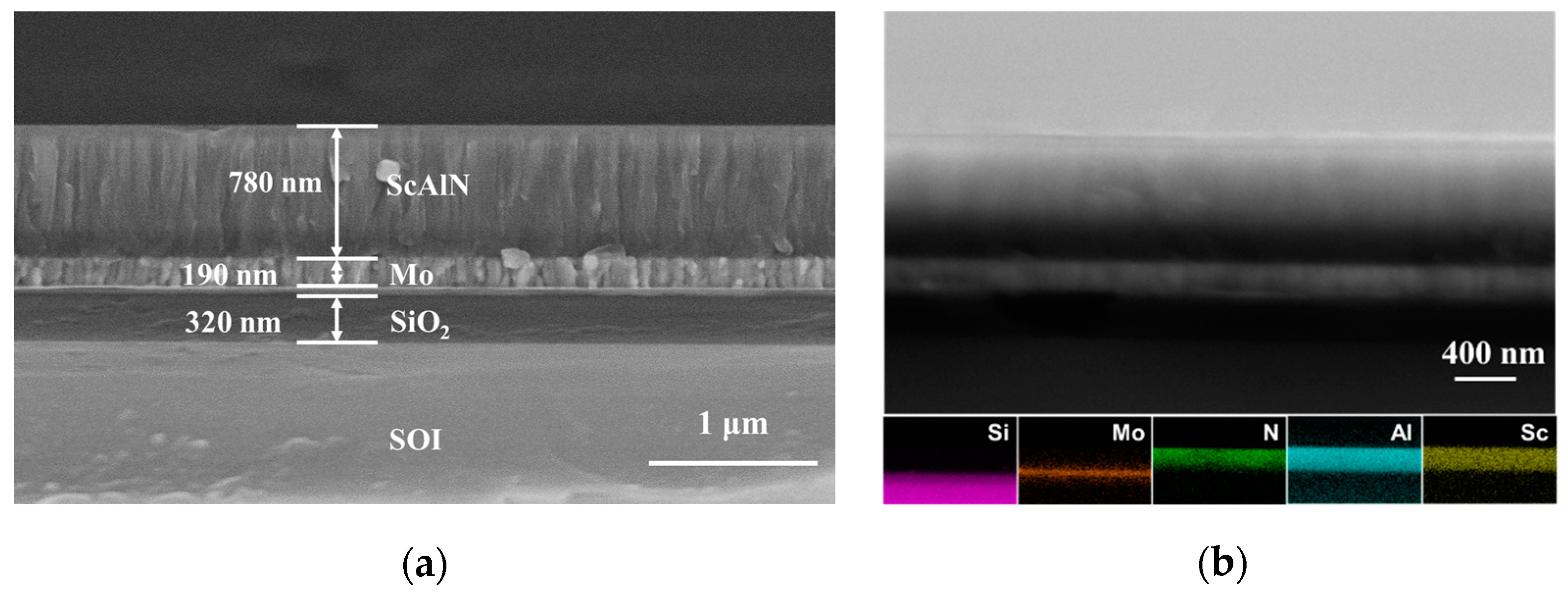
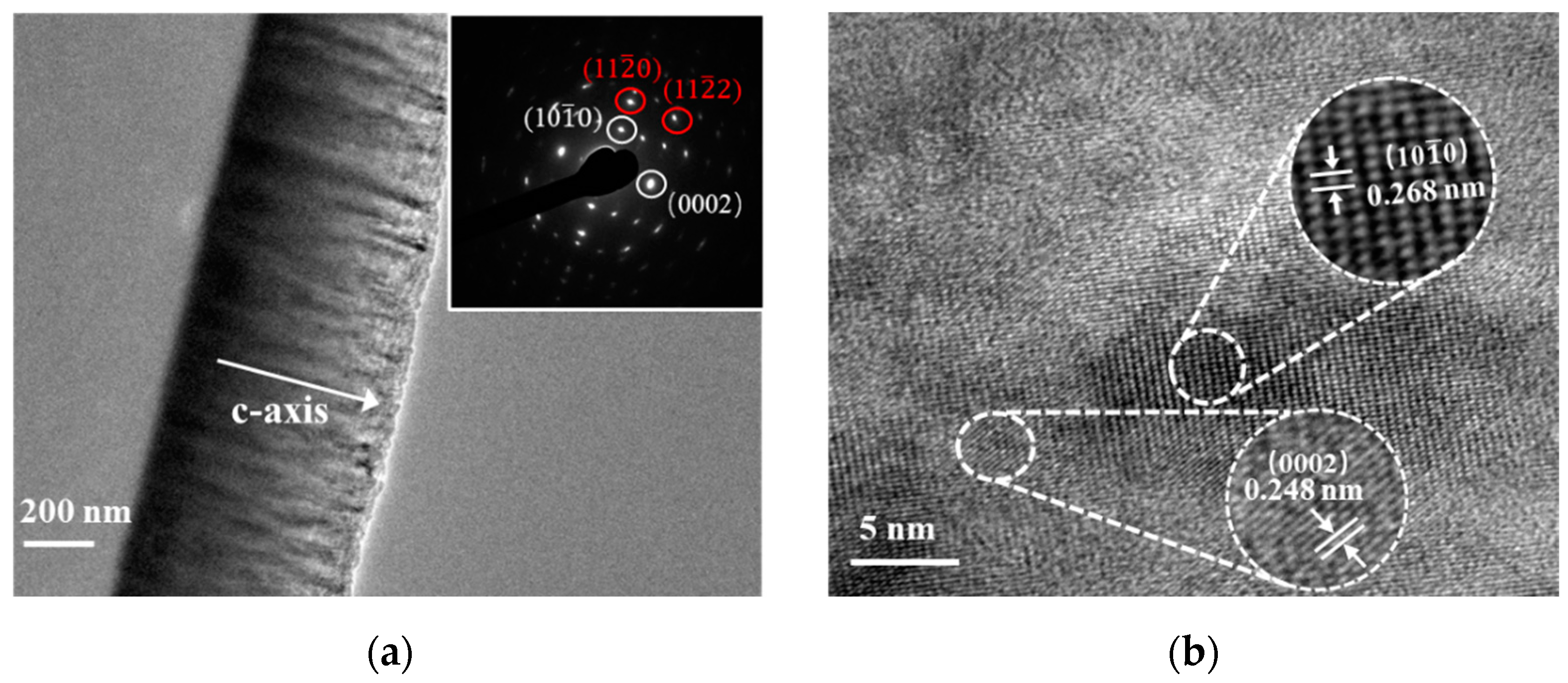
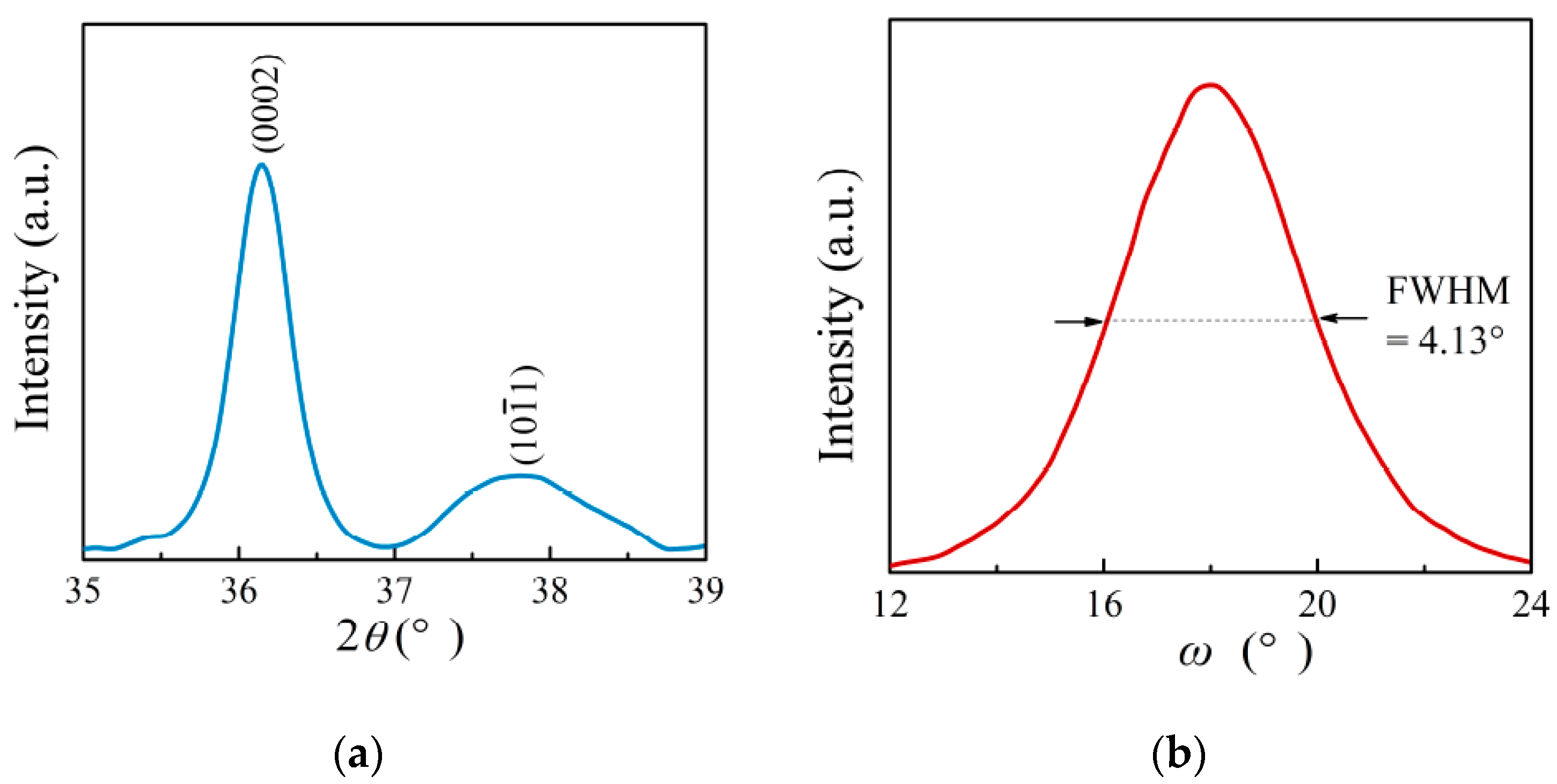
3.1. Microstructural and Crystal Structure Properties

Figure 1a shows the SEM cross-sectional view of the microstructure of the ScAlN thin film deposited on the Mo/SiO2/SOI substrate. The SEM image indicates that the prepared thin film had a visible columnar structure that grew perpendicular to the substrate. This columnar-like growth was similar to the columnar microstructure of pure AlN [28]. It can be observed that the SAlN thin film had a good crystalline quality and a clear grain boundary. The ScAlN thin film thickness was about 780 nm, and the thickness was about 190 and 320 nm for the Mo and SiO2, respectively. Figure 1b shows EDS mapping of the microstructure in a cross-sectional view. It shows that the prepared ScAlN film substrate had a layered structure; namely, ScAlN/Mo/SiO2/SOI, and the elements of Sc, Al, and N were evenly distributed in the ScAlN film. Through the EDS analysis, the atomic ratio for Sc:Al:N was found to be 0.29:0.71:1, which fit fairly well with the concentration of the Sc0.3-Al0.7 alloy target. This provided clear visual evidence that Al, N, and Sc elements were homogeneously distributed in the ScAlN.
Next, we turned to the detailed characterization of the crystal structure at the micro-nanometric level. Figure 2 illustrates the TEM plane views of the prepared Sc0.29Al0.71N thin film. It can be seen in Figure 2a, the cross-sectional TEM image, that the Sc0.29Al0.71N thin film had a uniform columnar structure and showed c-axis texture. The selective area electron diffraction (SAED) pattern (shown in the inset of Figure 2a) was composed of discrete spots in an arclike arrangement. Meanwhile, a slight spot broadening in the circumferential direction was present, which indicated that the crystalline quality of Sc0.29Al0.71N was not as good as the pure AlN thin film. It was noted that the crystal structure of Sc0.29Al0.71N was also found to have a hexagonal structure from the diffraction spots of the SAED pattern, and additional reflections such as (10 1 ¯ 0) and (11 2 ¯ 0) also appeared due to stacking faults. The HRTEM image of the same Sc0.29Al0.71N thin film (shown in Figure 2b) revealed that the crystal distortion and stacking faults occurred with the addition of Sc. The lattice plane spacing of the (0002) plane was about 0.248 nm, which was slightly smaller than that of the AlN (0.249 nm). A small amount of twinning with orientation (10 1 ¯ 0) was also visible, as the lattice parameters of (0002) and (10 1 ¯ 0) were very close to each other. These results indicated that the prepared Sc0.29Al0.71N thin film was polycrystalline.
The interplanar spacing of the hexagonal system is given by:
1 d 2 = 4 3 ( h 2 + h k + k 2 a 2 ) + l 2 c 2 ,
where h, k, and l are indices of the crystal plane; and d is the interplanar spacing. According to the obtained parameters shown in Figure 2, the a lattice constant and c lattice constant of the Sc0.29Al0.71N could be estimated as 3.0997 Å and 4.9569 Å, respectively. In order to further validate our results, we performed first-principles calculations on the structural properties of Sc0.29Al0.71N. Figure 3a shows the predicted crystal structure of the Sc0.29Al0.71N alloy. From the density of states (DOS) analysis shown in Figure 3b, we found that the Sc0.29Al0.71N remained semiconducting. The lattice parameter a in a pristine AlN crystal is defined as the distance between the N-N or Al-Al atoms within a hexagon ring. However, when the AlN was doped with Sc, the value of lattice parameter a varied due to localized strain. As shown in Table 2, in this work, the calculated value of a was taken as the average of all the N-N, Al-Al, Al-Sc, and N-Sc distances within the hexagon ring in a Sc0.29Al0.71N unit cell. The calculated lattice parameters of the crystal structure were a = 3.2619 Å and c = 4.9633 Å. These values were in good agreement with those previously reported Akiyama’s work, which were calculated using images of electron-beam diffractions [6].
Furthermore, X-ray photoelectron spectroscopy (XPS) was used to characterize the chemical bonds of the Sc-doped AlN thin film. Note that all XPS data were calibrated with 284.8 eV of C 1s peak. Figure 4a shows the Al 2p3/2 peak of the Sc0.29Al0.71N. The spectra exhibited only one intense peak related to aluminum, indicating that Al was the metal species with no inherent oxide. In Figure 4b, the nitrogen peak consists of two subpeaks of binding energies of 400.3 eV and 402.8 eV. The bigger subpeak at 402.8 eV was one belonging to the Al-N bond, and the smaller one was ascribed to the Sc-N bond. It can be seen that scandium had only one obvious peak in the Sc0.29Al0.71N thin film, indicating that there was only one way of binding Sc atoms. Through the analysis of the XPS, the data provided strong evidence that the Sc element formed a Sc-N combination in the Sc0.29Al0.71N thin film. It provided an effective basis for establishing a crystal structure model.

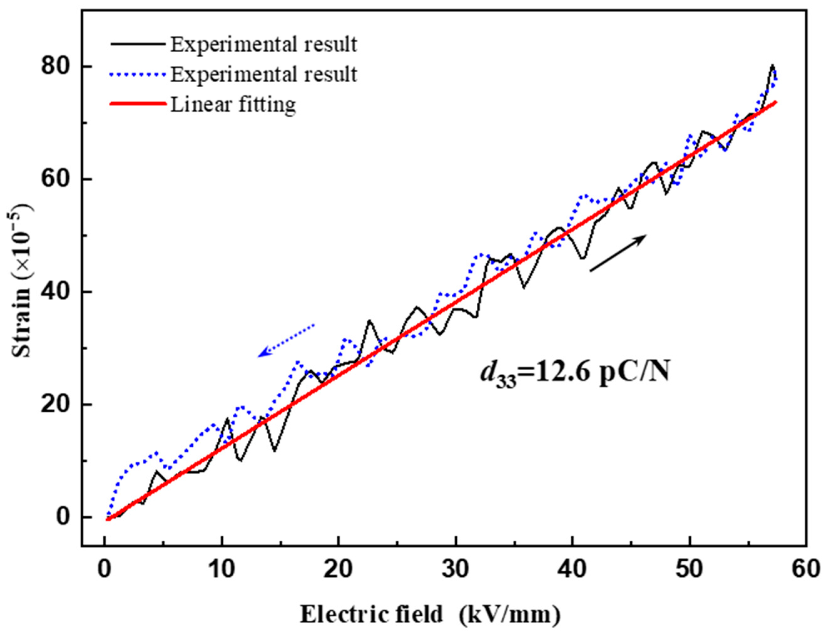
3.2. Crystal Orientation and Piezoelectric Properties

The crystal orientation of the Sc0.29Al0.71N thin film was investigated by HRXRD. The HRXRD measurements were carried out using the Cu Kα1 line (1.54056 Å). Figure 5a shows the HRXRD spectrum in θ–2θ scan mode of the Sc0.29Al0.71N thin film. There were two peaks of (0002) and (10 1 ¯ 1) in the 35–39° scanning range. In comparison, it showed a strong (0002) preferred orientation. Then, the crystallinity of thin films was investigated by XRD rocking-curve measurement. The full width at half maximum (FWHM) of the X-ray rocking curve is shown in Figure 5b. The FWHM value of the (0002) peak in the Sc0.29Al0.71N thin film was 4.13°. Although the crystal orientation was not high compared to that of single-crystal AlN film [29], this FWHM value suggested a strongly c-axis-oriented polycrystalline structure of the Sc0.29Al0.71N thin film.
Next, the ferroelectric hysteresis and field-induced strain curve of the Sc0.29Al0.71N thin film was investigated with a ferroelectric analyzer (Aixacct TF-2000). Figure 6 shows the measured field induced strain of the Sc0.29Al0.71N thin film as a function of an applied electric field. The experimental data showed that the induced strain varied linearly with both an increasing and decreasing electric field. An effective piezoelectric coefficient d33 of 12.6 pC/N could be estimated by linear fitting, which was slightly small compared to that of Akiyama’s work (~13.7 pC/N) [30]. This may have been caused by the difference in thin film quality or the different measurement tool. It is worth noting that the obtained d33 for Sc0.29Al0.71N thin film was almost 2.2 times larger than that of the AlN film. Such behaviors allowed us to know that it could be used in piezoelectric devices supporting strong electromechanical coupling. Taking an example of a surface acoustic wave resonator using the AlN film layered structure, in our previous work, the authors demonstrated that the effective coupling factor K2 was dramatically enhanced from 1.45% up to 10.5% by replacing AlN with ScAlN [31].

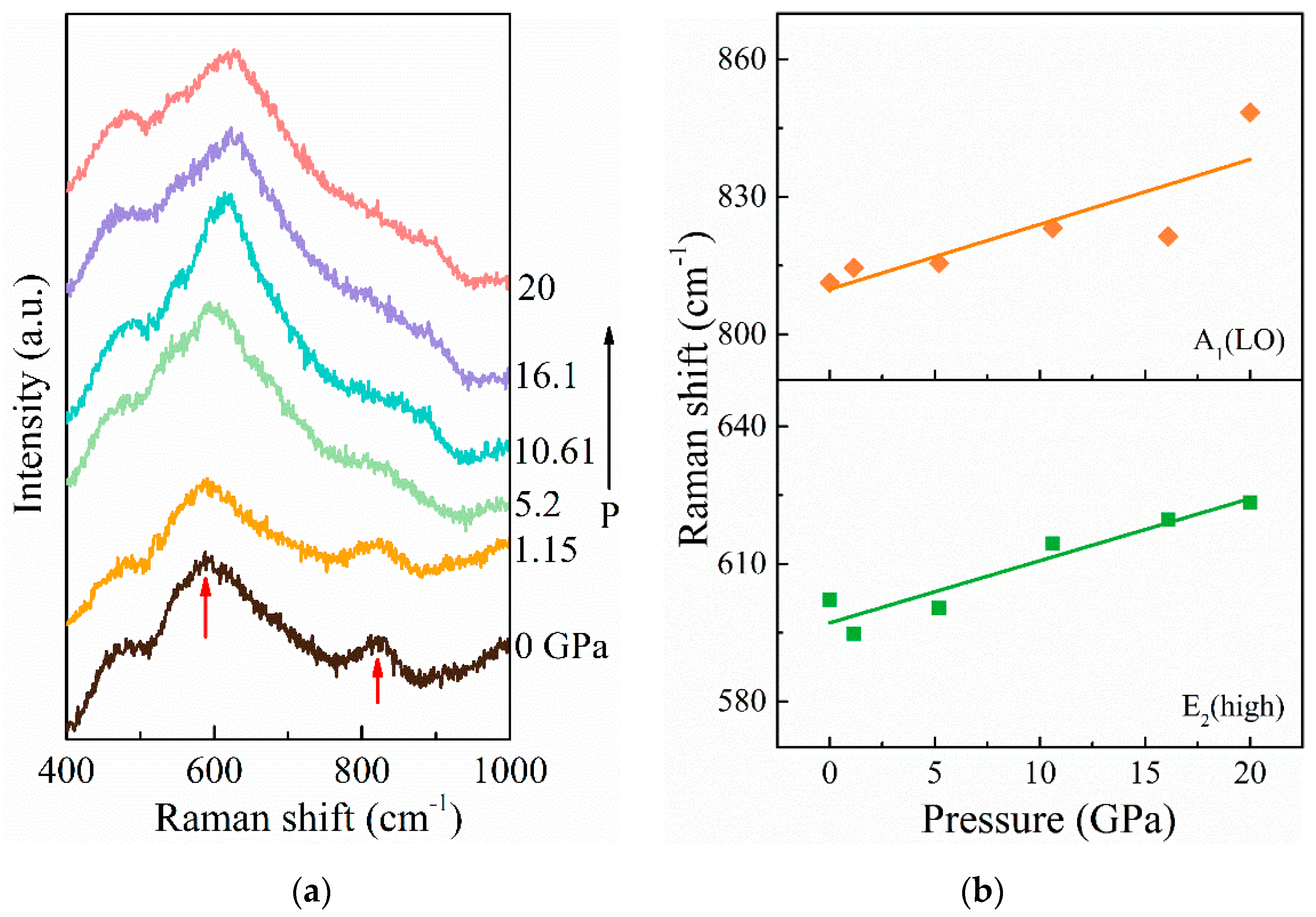
3.3. High-Pressure Properties

It is known that wurtzite-to-rocksalt phase transitions are typically observed in AlN at pressures of around 20 GPa [32]; nevertheless, ScAlN should be varied when doped with Sc. Hence, Raman measurements were taken of the Sc0.29Al0.71N thin film for analyses of its high-pressure properties. Figure 7a presents pressure-dependent Raman spectra of the Sc0.29Al0.71N thin film. The Raman spectra contained two peaks, at ~600 and ~810 cm−1, corresponding to the E2(high) and A1(LO) phonon modes, respectively [24,33]. It was found that the Raman bands of the wurtzite phase in AlN weakened above 18 GPa and disappeared at about 20 GPa due to the phase transition to the rocksalt structure [32,34,35]. However, it can be seen in Figure 7a that Raman bands in the Sc0.29Al0.71N thin film shifted continuously to higher phonon energy. No broadening or intensity loss of the E2(high) phonon mode was observed. The spectra were fitted with the Lorentz functions to determine the phonon wavenumber. The fitted results shown in Figure 7b were the measured frequencies for E2(high) and A1(LO) modes as a function of pressure, while the lines were obtained from linear fitting. With increasing pressure, the spectral deconvolution of the Raman spectra revealed a slightly linear enhancement in the frequency of phonon modes, and the decrease in lattice constants was related to the increase in phonon frequencies. Compared with the pressure dependence of the phonon frequencies of the Raman-active modes in wurtzite AlN, the rate of variation of frequencies with pressure for the E2(high) mode in Sc0.29Al0.71N was smaller. There was no wurtzite-to-rocksalt phase transition under high pressure (≤20 GPa). This means that piezoelectric devices using Sc0.29Al0.71N thin film could maintain material properties under high pressure, which is very important to ensure stable and reliable device performance, especially for piezoelectric pressure sensors.

4. Conclusions

In this work, a Sc0.29Al0.71N piezoelectric thin film measuring 780 nm thick was prepared with a conventional pulsed DC magnetron sputtering system on a Mo/SiO2/AlN/SOI substrate. Characterization of the microstructural and crystal structure properties for the sputtered Sc0.29Al0.71N thin film were performed. The SEM micrographs showed that the Sc0.29Al0.71N thin film had a good crystalline quality and a clear grain boundary. The TEM images revealed that crystal distortion and stacking faults occurred with the addition of Sc. The analyses of the XPS showed that the Sc element formed a Sc-N combination in the Sc0.29Al0.71N thin film. Analyses based on the DOS indicated that the Sc0.29Al0.71N remained semiconducting. The crystal structure was hexagonal phase, and the measured lattice constants a and c of Sc0.29Al0.71N were estimated as 3.0997 Å and 4.9569 Å, respectively. First-principles calculations were performed to predict the structural and electronic properties of the Sc0.29Al0.71N. The calculated lattice parameters were in good agreement with the measured results. This provided an effective basis for establishing a crystal structure model of ScxAl1−xN for various Sc content.
Furthermore, the piezoelectric-device-relevant material properties in terms of crystal orientation and piezoelectric response, as well as high-pressure properties, were also investigated. The results demonstrated that the prepared ScAlN thin film offered high-quality crystal orientation and a high effective piezoelectric coefficient d33 of 12.6 pC/N. In addition, there was no wurtzite-to-rocksalt phase transition under high pressure (≤20 GPa), which is quite beneficial for application in strong coupling piezoelectric devices with high-pressure stability.

Author Contributions

Conceptualization, X.S., Q.Z. and X.Z.; methodology on DFT and related calculations, K.H.Y. and K.-H.C.; formal analysis, K.H.Y., M.C., and H.L.; investigation, Q.Z., X.Q., F.W., and X.Z.; resources, X.S. and X.Q.; data curation, F.W. and Y.T.; writing—original draft preparation, Q.Z. and M.C.; writing—review and editing, Q.Z., K.-H.C., and X.Z.; visualization, M.C. and H.L.; supervision, Q.Z. and Y.T.; project administration, X.Z.; funding acquisition, Q.Z., F.W. and X.Z. All authors have read and agreed to the published version of the manuscript.

Funding

This research was funded by the National Natural Science Youth Foundation of China (Grant Number 11904233), the National Natural Science Foundation of China (Grant Number 52172005), and the Science and Technology Commission of Shanghai Municipality (Grant Number 19070502800).

Institutional Review Board Statement

Not applicable.

Informed Consent Statement

Not applicable.

Data Availability Statement

Data sharing is not applicable for this article.

Acknowledgments

The authors would like to thank the Center for High Pressure Science and Technology Advanced Research (HPSTAR, Shanghai) for providing the high-pressure experimental setup. The authors would also like to thank Hao Deng from the Institute of Crystallography, RWTH Aachen University of Germany, for the valuable crystal structural discussion.

Conflicts of Interest

The authors declare no conflict of interest.

References

  1. Mariotti, G.; Vannozzi, L. Fabrication, characterization, and properties of poly (ethylene-co-vinyl acetate) composite thin films doped with piezoelectric nanofillers. Nanomaterials 2019, 9, 1182. [Google Scholar] [CrossRef] [Green Version]
  2. Jin, C.; Hao, N.; Xu, Z.; Trase, I.; Nie, Y.; Dong, L.; Closson, A.; Chen, Z.; Zhang, J.X.J. Flexible piezoelectric nanogenerators using metal-doped ZnO-PVDF films. Sens. Actuators A 2020, 305, 111912. [Google Scholar] [CrossRef] [PubMed]
  3. Talbi, A.; Sarry, F.; Brizoual, L.L.; Elmazria, O.; Alnot, P. Sezawa mode SAW pressure sensors based on ZnO/Si structure. IEEE Trans. Ultrason. Ferroelect. Freq. Control 2004, 51, 1421–1426. [Google Scholar] [CrossRef]
  4. Dubois, M.-A.; Muralt, P. Properties of aluminum nitride thin films for piezoelectric transducers and microwave filter applications. Appl. Phys. Lett. 1999, 74, 3032–3034. [Google Scholar] [CrossRef]
  5. Tadigadapa, S.; Mateti, K. Piezoelectric MEMS sensors: State-of-the-art and perspectives. Meas. Sci. Technol. 2009, 20, 092001. [Google Scholar] [CrossRef]
  6. Akiyama, M.; Kamohara, T.; Kano, K.; Teshigahara, A.; Takeuchi, Y.; Kawahara, N. Enhancement of piezoelectric response in scandium aluminum nitride alloy thin films prepared by dual reactive cosputtering. Adv. Mater. 2009, 21, 593–596. [Google Scholar] [CrossRef] [PubMed]
  7. Wingqvist, G.; Tasnadi, F.; Zukauskaite, A.; Birch, J.; Arwin, H.; Hultman, L. Increased electromechanical coupling in w−ScxAl1−xN. Appl. Phys. Lett. 2010, 97, 112902. [Google Scholar] [CrossRef]
  8. Piazza, G.; Felmetsger, V.; Muralt, P.; Olsson, R.H.; Ruby, R. Piezoelectric aluminum nitride thin films for microelectromechanical systems. MRS Bull. 2012, 37, 1051–1061. [Google Scholar] [CrossRef] [Green Version]
  9. Yantchev, V.; Katardjiev, I. Thin film Lamb wave resonators in frequency control and sensing applications: A review. J. Micromech. Microeng. 2013, 23, 043001. [Google Scholar] [CrossRef]
  10. Takeuchi, N. First-principles calculations of the ground-state properties and stability of ScN. Phys. Rev. B 2002, 65, 045204. [Google Scholar] [CrossRef]
  11. Zoroddu, A.; Bernardini, F.; Ruggerone, P.; Fiorentini, V. First-principles prediction of structure, energetics, formation enthalpy, elastic constants, polarization, and piezoelectric constants of AlN, GaN, and InN: Comparison of local and gradient-corrected density-functional theory. Phys. Rev. B 2001, 64, 045208. [Google Scholar] [CrossRef] [Green Version]
  12. Mancera, L.; Rodríguez, J.A.; Takeuchi, N. Theoretical study of the stability of wurtzite, zinc-blende, NaCl and CsCl phases in group IIIB and IIIA nitrides. Phys. Status Solidi. B 2004, 241, 2424. [Google Scholar] [CrossRef]
  13. Farrer, N.; Bellaiche, L. Properties of Hexagonal ScN versus Wurtzite GaN and InN. Phys. Rev. B 2002, 66, 201203. [Google Scholar] [CrossRef]
  14. Ranjan, V.; Bin-Omran, S.; Sichuga, D.; Nichols, R.S.; Bellaiche, L.; Alsaad, A. Properties of GaN/ScN and InN/ScN superlattices from first principles. Phys. Rev. B 2005, 72, 085315. [Google Scholar] [CrossRef]
  15. Alsaad, A.; Ahmad, A. Piezoelectricity of ordered (ScxGa1−xN) alloys from first principles. Eur. Phys. J. 2006, 54, 151–156. [Google Scholar] [CrossRef]
  16. Wang, Q.; Lu, Y.; Mishin, S.; Oshmyansky, Y.; Horsley, D.A. Design, fabrication, and characterization of scandium aluminum nitride-based piezoelectric micromachined ultrasonic transducers. J. Microelectromech. Syst. 2017, 26, 1132. [Google Scholar] [CrossRef]
  17. Moreira, M.; Bjurström, J.; Katardjev, I.; Yantchev, V. Aluminum scandium nitride thin-film bulk acoustic resonators for wide band applications. Vacuum 2011, 86, 23–26. [Google Scholar] [CrossRef]
  18. Hashimoto, K.; Sato, S.; Teshigahara, A.; Nakamura, T.; Kano, K. High-performance surface acoustic wave resonators in the 1 to 3 GHz range using a ScAlN/6H-SiC structure. IEEE Trans. Ultrason. Ferroelect. Freq. Control 2013, 60, 637–642. [Google Scholar] [CrossRef]
  19. Hardy, M.T.; Downey, B.P.; Nepal, N.; Storm, D.F.; Katzer, D.S.; Meyer, D.J. Epitaxial ScAlN grown by molecular beam epitaxy on GaN and SiC substrates. Appl. Phys. Lett. 2017, 110, 162104. [Google Scholar] [CrossRef]
  20. Sumisaka, M.; Yamazaki, K.; Fujii, S.; Tang, G.; Han, T.; Suzuki, Y.; Otomo, S.; Omori, T.; Hashimoto, K. Sputter deposition of ScAlN using large size alloy target with high Sc content and reduction of Sc content in deposited films. Jpn. J. Appl. Phys. 2015, 54, 07HD06. [Google Scholar] [CrossRef]
  21. Li, X.-H.; Wang, S.; Xie, H.; Wei, Y.O.; Kao, T.-T.; Satter, M.M.; Shen, S.-C.; Douglas Yoder, P.; Detchprohm, T.; Dupuis, R.D.; et al. Growth of high-quality AlN layers on sapphire substrates at relatively low temperatures by metalorganic chemical vapor deposition. Phys. Status Solidi B 2015, 252, 1089–1095. [Google Scholar] [CrossRef]
  22. Arakawa, K.; Yanagitani, T.; Kano, K.; Teshigahara, A.; Akiyama, M. Deposition techniques of c-axis-tilted ScAlN films by conventional RF magnetron sputtering. In Proceedings of the 2010 IEEE International Ultrasonics Symposium, San Diego, CA, USA, 11–14 October 2010; pp. 1050–1053. [Google Scholar] [CrossRef]
  23. Zukauskaite, A.; Wingqvist, G.; Palisaitis, J.; Jensen, J.; Persson, P.O.Å.; Matloub, R.; Muralt, P.; Kim, Y.; Birch, J.; Hultman, L. Microstructure and dielectric properties of piezoelectric magnetron sputtered w-ScxAl1−xN thin films. J. Appl. Phys. 2012, 111, 093527. [Google Scholar] [CrossRef] [Green Version]
  24. Deng, R.; Jiang, K.; Gall, D. Optical phonon modes in ScxAl1−xN. J. Appl. Phys. 2014, 115, 013506. [Google Scholar] [CrossRef]
  25. Giannozzi, P.; Baroni, S.; Bonini, N.; Calandra, M.; Car, R.; Cavazzoni, C.; et al. QUANTUM ESPRESSO: A modular and open-source software project for quantum simulations of materials. J. Phys. Condens. Matter. 2009, 21, 395502. [Google Scholar] [CrossRef]
  26. Giannozzi, P.; Andreussi, O.; Brumme, T.; Bunau, O.; Nardelli, M.B.; Calandra, M.; et al. Advanced capabilities for materials modelling with Quantum ESPRESSO. J. Phys. Condens. Matter 2017, 29, 465901. [Google Scholar] [CrossRef] [PubMed] [Green Version]
  27. Perdew, J.P.; Ruzsinszky, A.; Csonka, G.I.; Vydrov, O.A.; Scuseria, G.E.; Constantin, L.A.; Zhou, X.; Burke, K. Restoring the density-gradient expansion for exchange in solids and surfaces. Phys. Rev. Lett. 2008, 100, 136406. [Google Scholar] [CrossRef] [PubMed] [Green Version]
  28. Lloret, F.; Araújo, D.; Villar, M.P.; Rodríguez-Madrid, J.G.; Iriarte, G.F.; Williams, O.A.; Calle, F. Diamond underlayer microstructure effect on the orientation of AlN piezoelectric layers for high frequency SAW resonators by TEM. Microelectron. Eng. 2013, 112, 193–197. [Google Scholar] [CrossRef]
  29. Okano, H.; Takahashi, Y.; Tanaka, T.; Shibata, K.; Nakano, S. Preparation of c-Axis oriented AlN thin films by low-temperature reactive sputtering. Jpn. J. Appl. Phys. 1992, 31, 3446. [Google Scholar] [CrossRef]
  30. Akiyama, M.; Kano, K.; Teshigahara, A. Influence of growth temperature and scandium concentration on piezoelectric response of scandium aluminum nitride alloy thin films. Appl. Phys. Lett. 2009, 95, 162107. [Google Scholar] [CrossRef]
  31. Zhang, Q.; Han, T.; Tang, G.; Chen, J.; Hashimoto, K.Y. SAW characteristics of AlN/SiO2/3C-SiC layered structure with embedded electrodes. IEEE Trans. Ultrason. Ferroelect. Freq. Control 2016, 63, 1608–1612. [Google Scholar] [CrossRef]
  32. Manjón, F.J.; Errandonea, D.; Romero, A.H.; Garro, N.; Serrano, J.; Kuball, M. Lattice dynamics of wurtzite and rocksalt AlN under high pressure: Effect of compression on the crystal anisotropy of wurtzite-type semiconductors. Phys. Rev. B 2008, 77, 205204. [Google Scholar] [CrossRef] [Green Version]
  33. Kuball, M.; Hayes, J.M.; Prins, A.D.; Uden, N.W.V.; Dunstan, D.J.; Shi, Y.; Edgar, J.H. Raman scattering studies on single-crystalline bulk AlN under high pressures. Appl. Phys. Lett. 2001, 78, 724. [Google Scholar] [CrossRef]
  34. Kuball, M.; Hayes, J.M.; Shi, Y.; Edgar, J.H.; Prins, A.D.; Uden, N.W.A.; Dunstan, D.J. Raman scattering studies on single-crystalline bulk AlN: Temperature and pressure dependence of the AlN phonon modes. J. Cryst. Growth 2001, 231, 391. [Google Scholar] [CrossRef]
  35. Yakovenko, E.; Gauthier, M.; Polian, A. High-pressure behavior of the bond-bending mode of AIN. Exp. Theor. Phys. 2004, 98, 981. [Google Scholar] [CrossRef]
Figure 1. SEM micrographs and analysis of ScAlN thin film deposited on Mo/SiO2/AlN/SOI: (a) SEM micrographs; (b) EDS mapping.
Materials 14 06437 g001
Figure 2. TEM images of the prepared Sc0.29Al0.71N thin film: (a) cross-sectional TEM image and selective area electron diffraction pattern (SAED); (b) high-resolution TEM image.
Materials 14 06437 g002
Figure 3. (a) Top and side views of the calculated crystal structure; and (b) density of states (DOS) for the Sc0.29Al0.71N crystal. The purple, grey, and bluish spheres denote Al, N, and Sc atoms, respectively.
Materials 14 06437 g003
Figure 4. XPS elemental spectra for Sc0.29Al0.71N thin film: (a) Al 2p3/2; (b) N 1s and Sc 2p3/2.
Materials 14 06437 g004
Figure 5. (a) High-resolution XRD pattern and (b) X-ray rocking curve of the Sc0.29Al0.71N thin film.
Materials 14 06437 g005
Figure 6. The measured field-induced strain of the Sc0.29Al0.71N thin film as a function of an applied electric field.
Materials 14 06437 g006
Figure 7. (a) Pressure evolution of Raman spectra of the Sc0.29Al0.71N thin film for pressurization cycle; (b) pressure dependence of E2(high) and A1(LO) phonon modes.
Materials 14 06437 g007
Table 1. The deposition conditions.
ParameterValue
Target-substrate distance70 mm (fixed)
Substrate temperature300 °C
Power7500 W
RF Bias60W
Total gas pressure2.6 mTorr
Gas composition ratioAr/N2 = 1/3
Sputtering time20 min
Table 2. The calculated lattice constants within a unit cell of Sc0.29Al0.71N.
Lattice Constant, a (Å)
3.47923.13563.16163.15783.59573.0657
3.22373.18893.21353.35153.15513.2530
3.13763.53823.15463.14983.14033.5532
3.19533.35103.25783.15453.23883.2537
3.12573.10103.45243.59653.08943.1694
3.34653.22123.23443.16323.32683.2614
3.18203.17443.43803.10183.53493.1677
3.23873.24433.37733.24243.36733.1387
3.52423.06463.27143.15213.08023.2563
3.24323.39383.15593.31913.24013.1299
3.17813.52843.22953.54103.15663.1619
3.36123.17693.26903.22733.18313.2497
3.25993.15573.37343.33103.24453.2025
3.60093.41513.18113.22863.14193.4969
3.09743.14563.30843.22093.43483.1904
Note: The average and standard deviations of the calculated lattice constant a were 3.2619 Å and 0.1382 Å, respectively.
Publisher’s Note: MDPI stays neutral with regard to jurisdictional claims in published maps and institutional affiliations.

