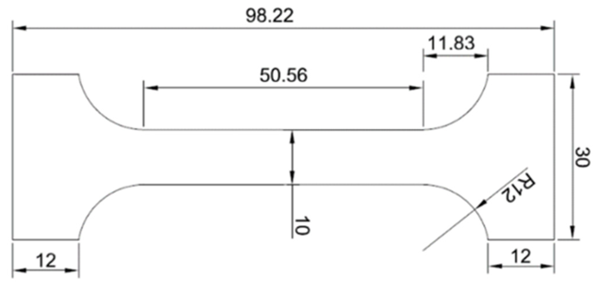
Figure 1.
Test piece of a solder for a static tensile test.
Figure 1.
Test piece of a solder for a static tensile test.
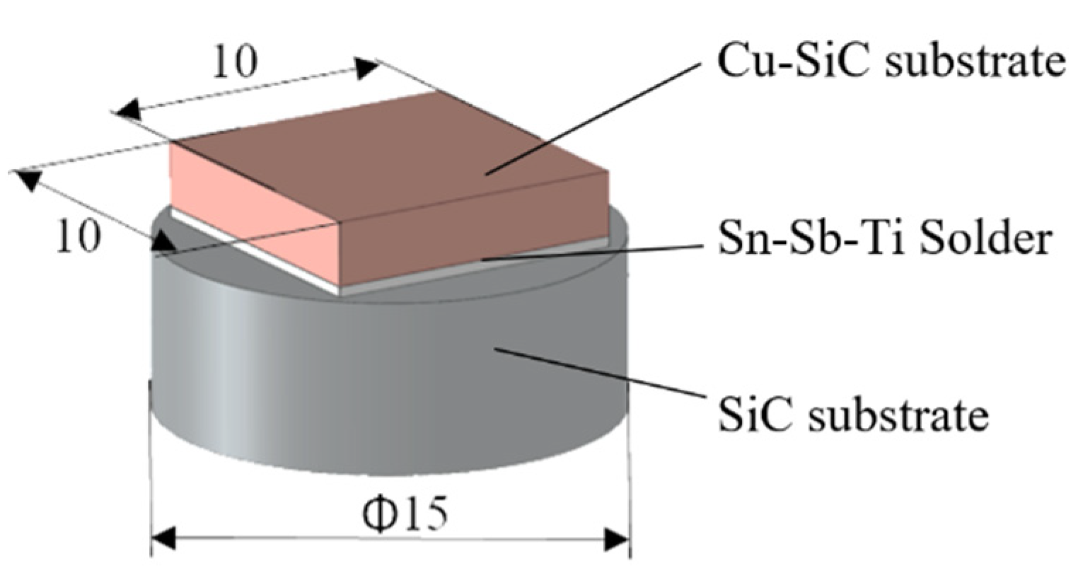
Figure 2.
Microstructure of a metal–ceramic composite of the type Cu–SiC.
Figure 2.
Microstructure of a metal–ceramic composite of the type Cu–SiC.
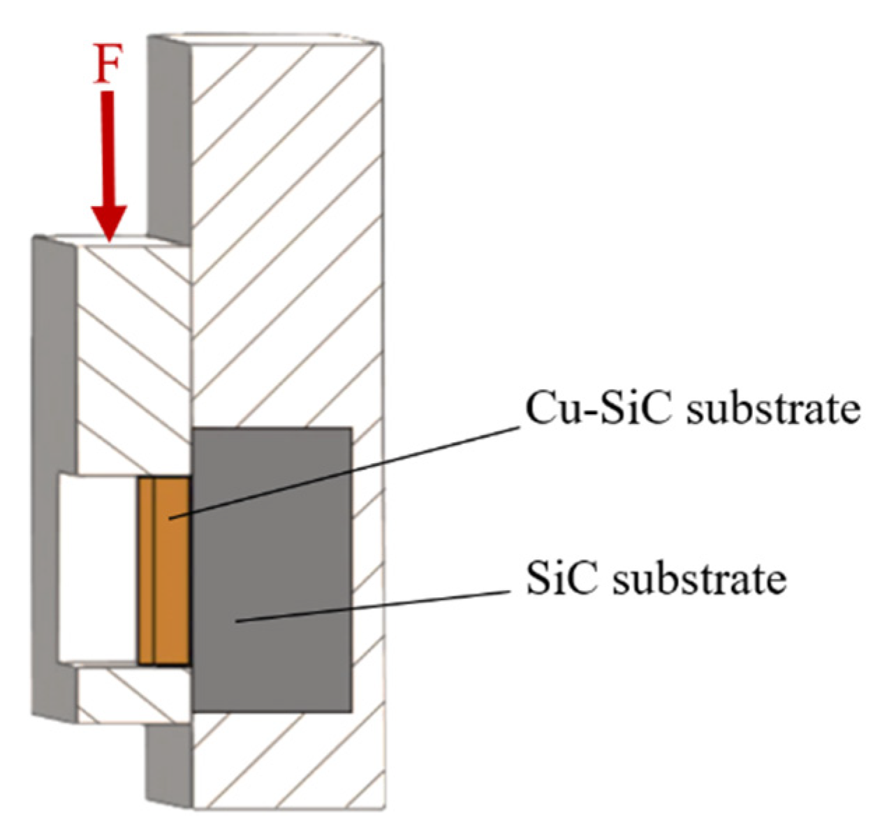
Figure 3.
Assembly of a soldered joint for analysis of solder/substrate boundaries.
Figure 3.
Assembly of a soldered joint for analysis of solder/substrate boundaries.
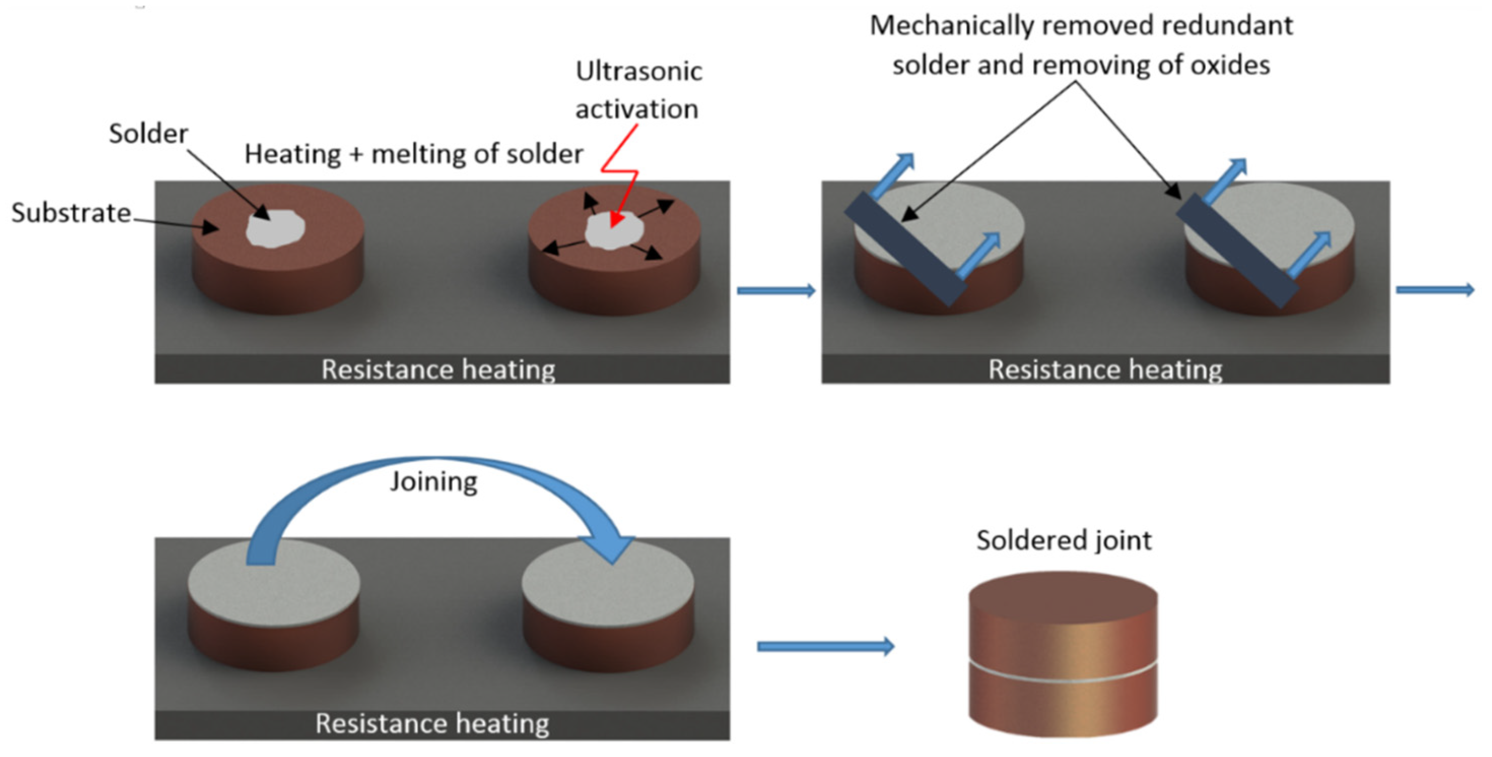
Figure 4.
Schematic representation of the soldering process in the presence of ultrasonic power.
Figure 4.
Schematic representation of the soldering process in the presence of ultrasonic power.
Figure 5.
Schematic representation of the specimen for the shear strength test of the Cu–SiC/Sb–Sb–Ti/SiC joint.
Figure 5.
Schematic representation of the specimen for the shear strength test of the Cu–SiC/Sb–Sb–Ti/SiC joint.
Figure 6.
Scheme of shear strength measurement.
Figure 6.
Scheme of shear strength measurement.
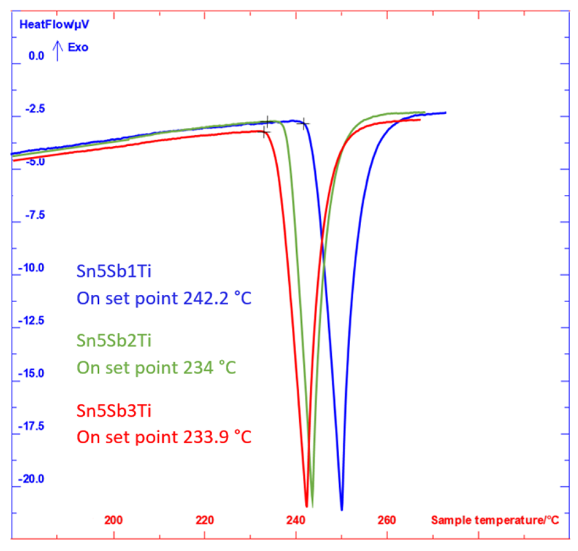
Figure 7.
DTA analysis of specimens of soldering alloys of the type SnSb5TiX (2nd measurement).
Figure 7.
DTA analysis of specimens of soldering alloys of the type SnSb5TiX (2nd measurement).
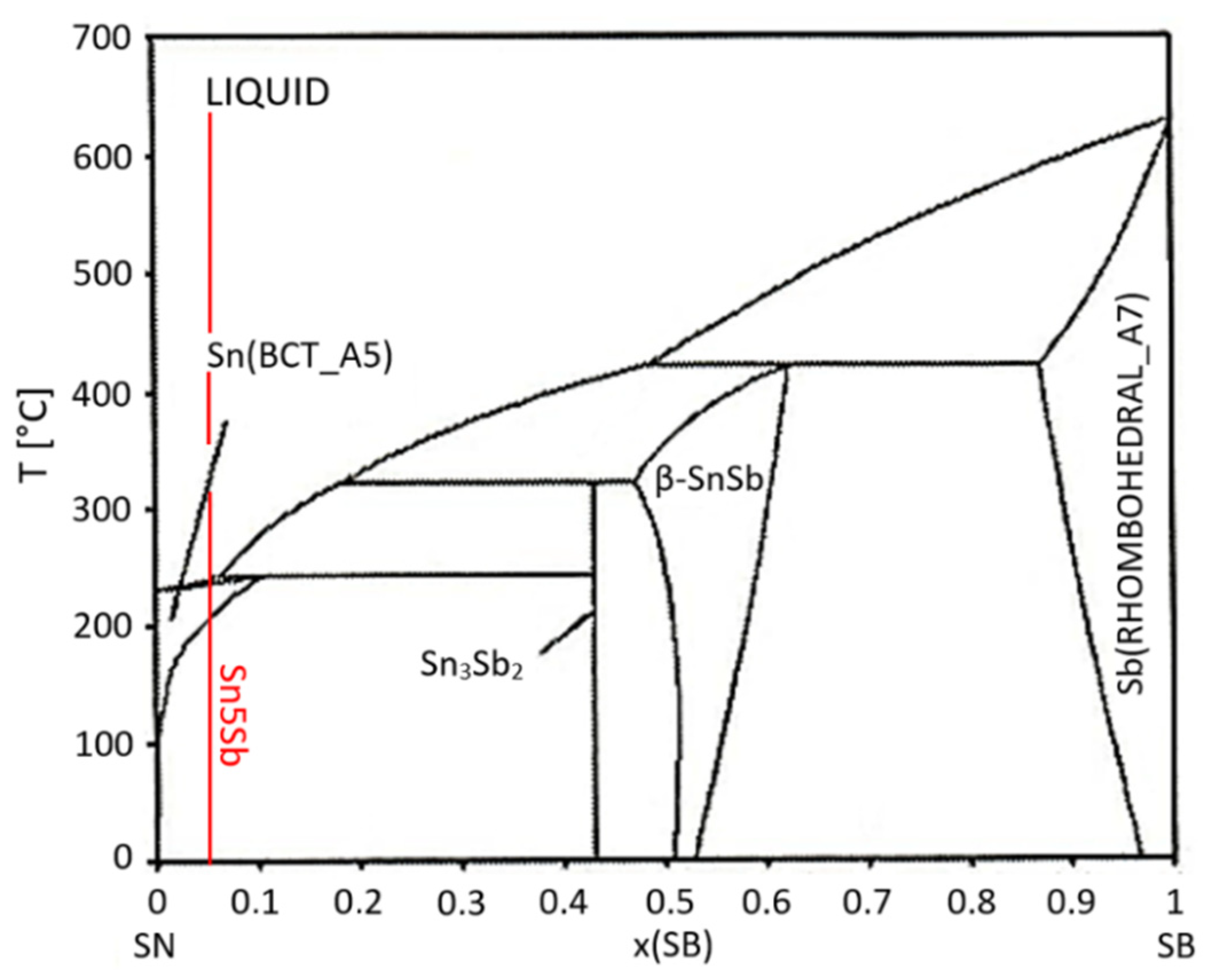
Figure 8.
Binary system of tin–antimony [
38]. The red line indicates the chemical composition of the Sn5Sb base solder.
Figure 8.
Binary system of tin–antimony [
38]. The red line indicates the chemical composition of the Sn5Sb base solder.
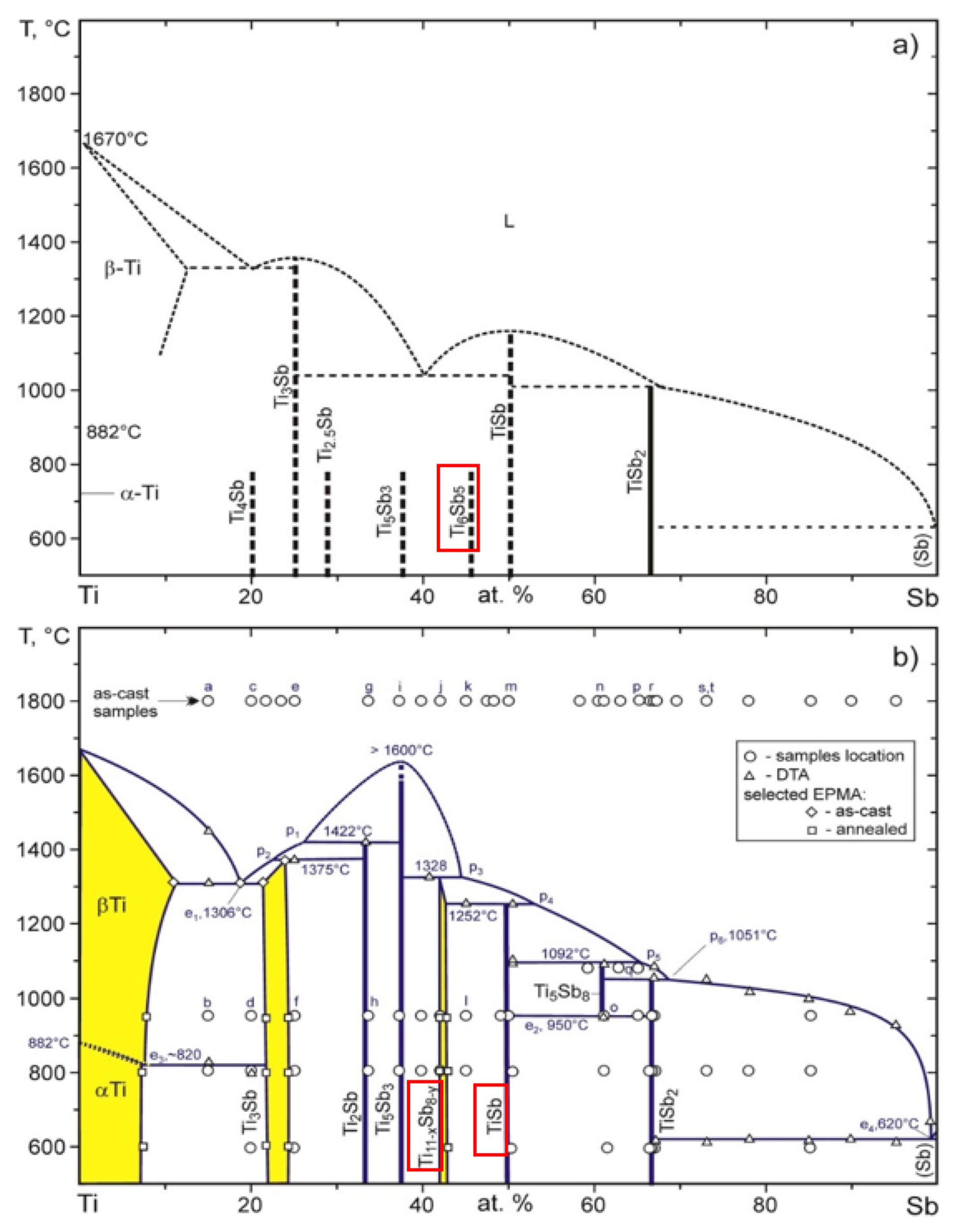
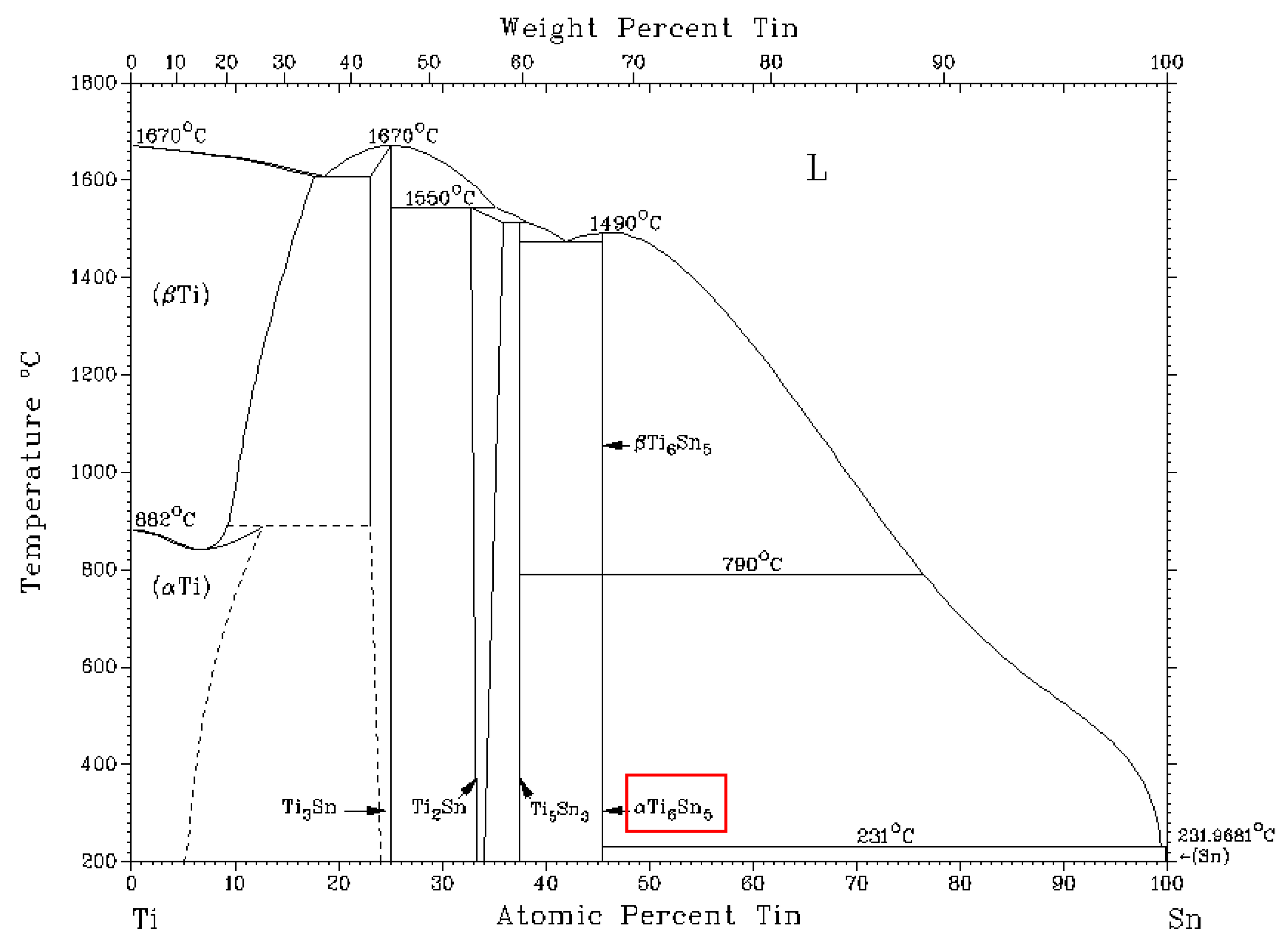
Figure 9.
Equilibrium binary diagram of the tin-titanium system [
39]. The red box indicates the phase identified in the solder structure.
Figure 9.
Equilibrium binary diagram of the tin-titanium system [
39]. The red box indicates the phase identified in the solder structure.
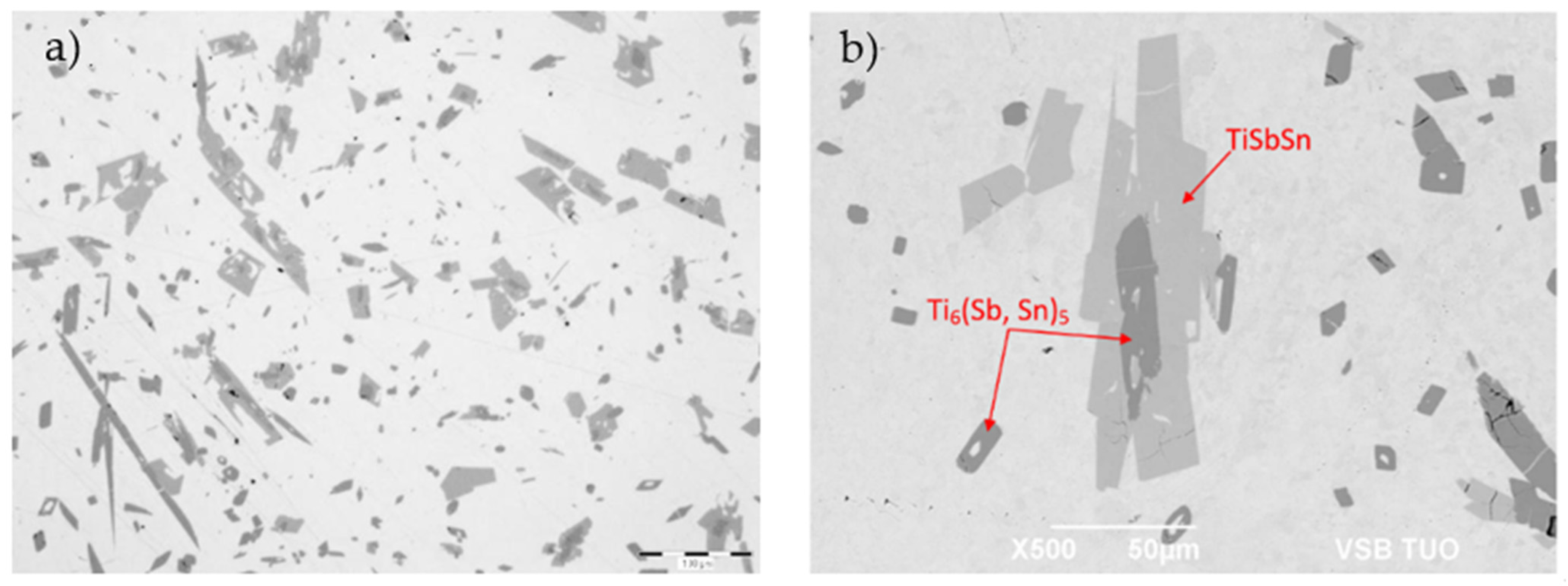
Figure 10.
Microstructure of the Sn5Sb3Ti phase; (a) from an optical microscope in the as-etched condition; (b) from SEM in BSE mode at a higher magnification.
Figure 10.
Microstructure of the Sn5Sb3Ti phase; (a) from an optical microscope in the as-etched condition; (b) from SEM in BSE mode at a higher magnification.
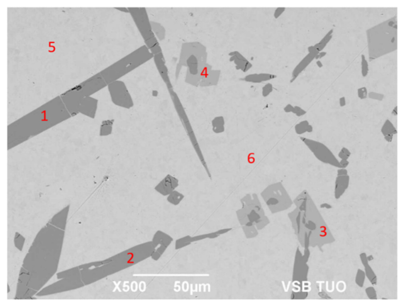
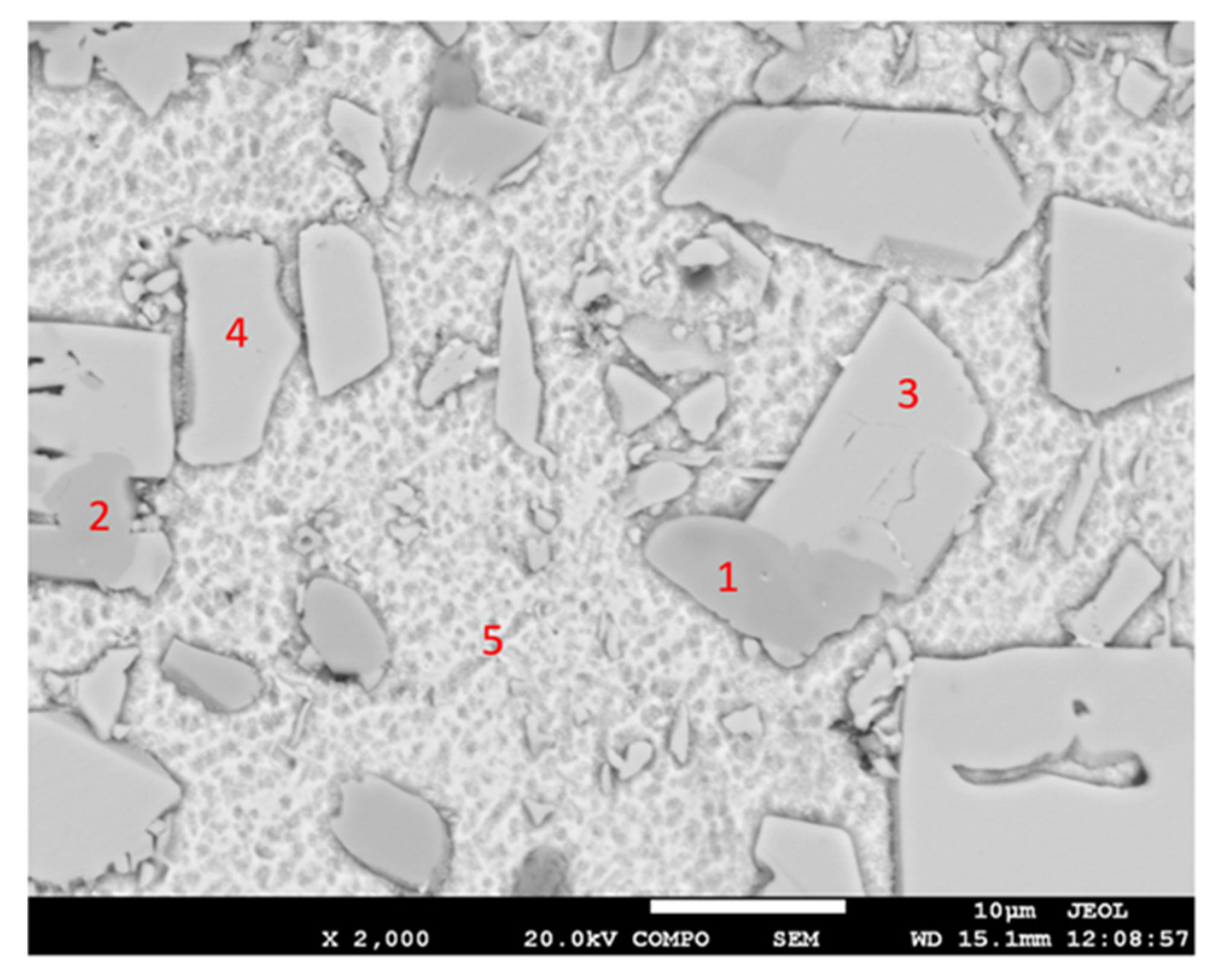
Figure 11.
Representation of measuring points of the Sn5Sb3Ti solder.
Figure 11.
Representation of measuring points of the Sn5Sb3Ti solder.
Figure 12.
Equilibrium diagram of titanium—antimony; (
a) partial [
40]; (
b) completed [
40].
Figure 12.
Equilibrium diagram of titanium—antimony; (
a) partial [
40]; (
b) completed [
40].
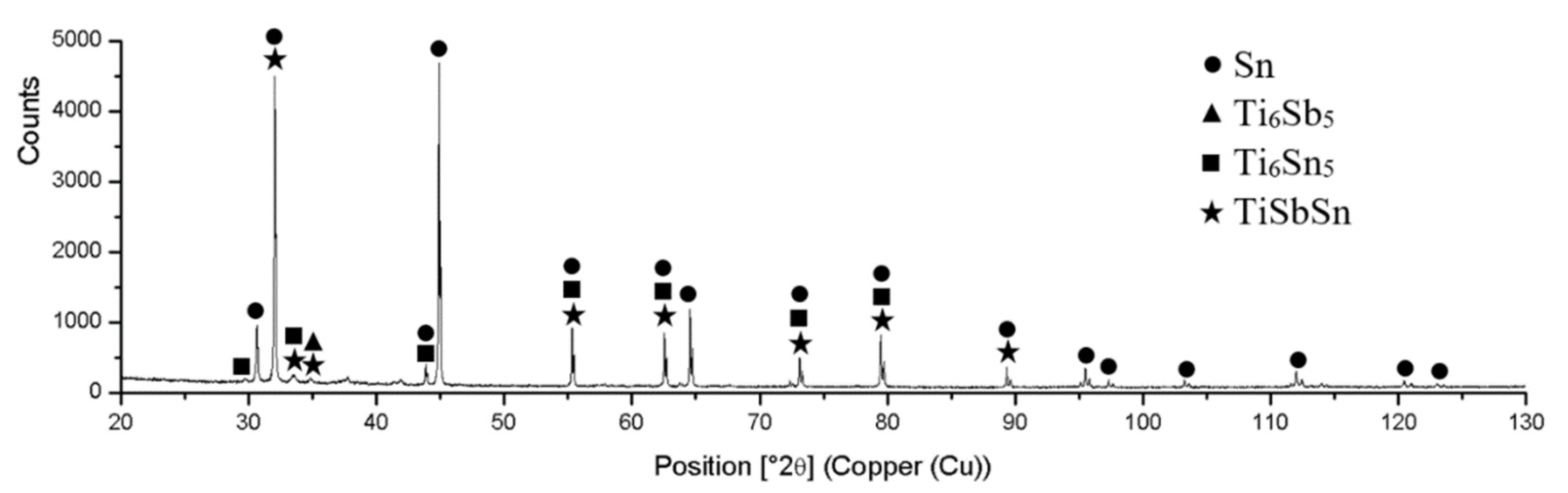
Figure 13.
XRD analysis of the Sn5Sb3Ti solder.
Figure 13.
XRD analysis of the Sn5Sb3Ti solder.
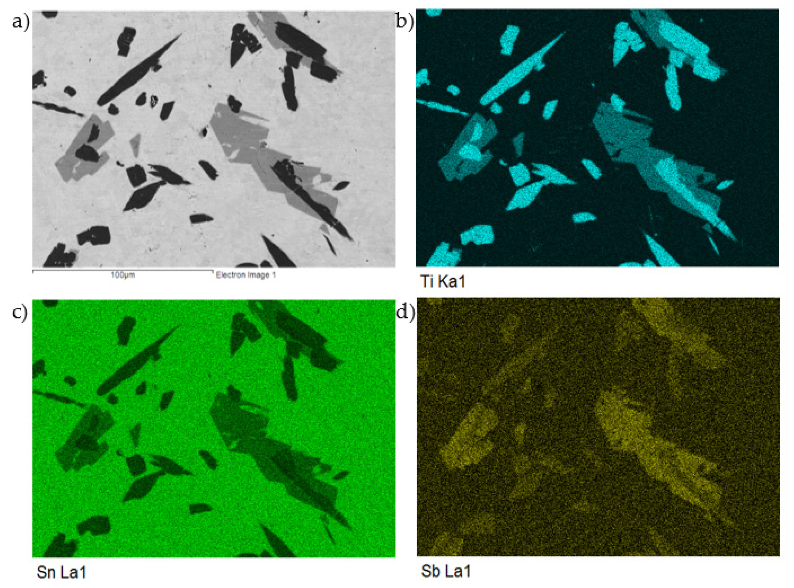
Figure 14.
The map of Ti, Sn, and Sb elements in the microstructure of the SnSb5Ti3 solder. SEM photo of (a) the microstructure, (b) Ti, (c) Sn, and (d) Sb.
Figure 14.
The map of Ti, Sn, and Sb elements in the microstructure of the SnSb5Ti3 solder. SEM photo of (a) the microstructure, (b) Ti, (c) Sn, and (d) Sb.
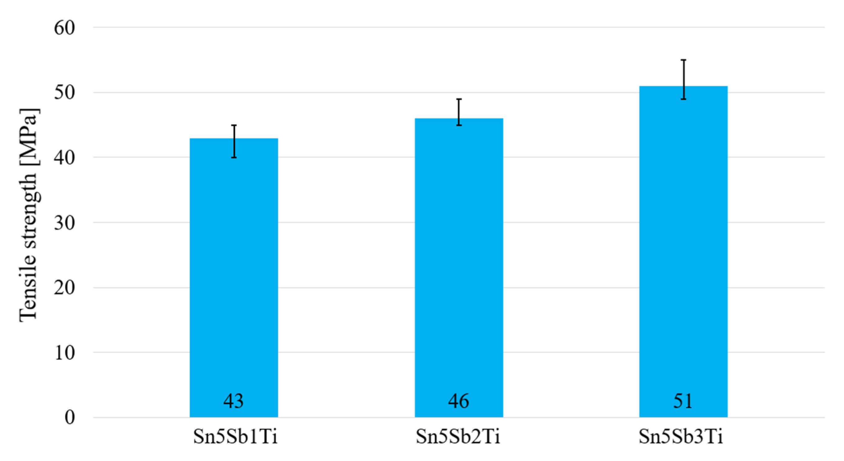
Figure 15.
Tensile strength of soldering alloys of the type Sn5Sb1-3Ti.
Figure 15.
Tensile strength of soldering alloys of the type Sn5Sb1-3Ti.
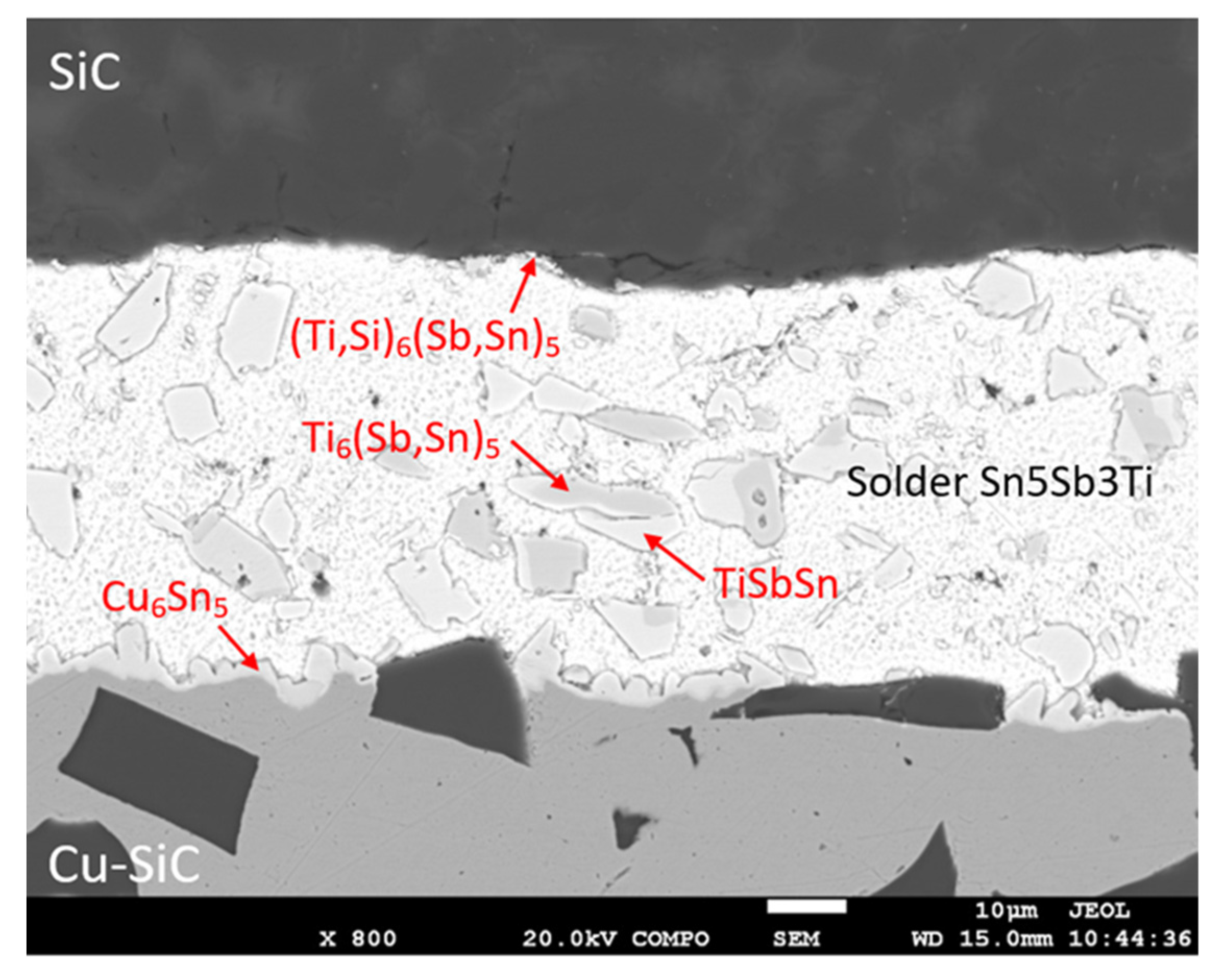
Figure 16.
Microstructure of the SiC/Sn5Sb3Ti/Cu–SiC joint from the SEM analysis in BSE mode.
Figure 16.
Microstructure of the SiC/Sn5Sb3Ti/Cu–SiC joint from the SEM analysis in BSE mode.
Figure 17.
Representation of measuring points of the SiC/Sn5Sb3Ti/Cu–SiC joint.
Figure 17.
Representation of measuring points of the SiC/Sn5Sb3Ti/Cu–SiC joint.
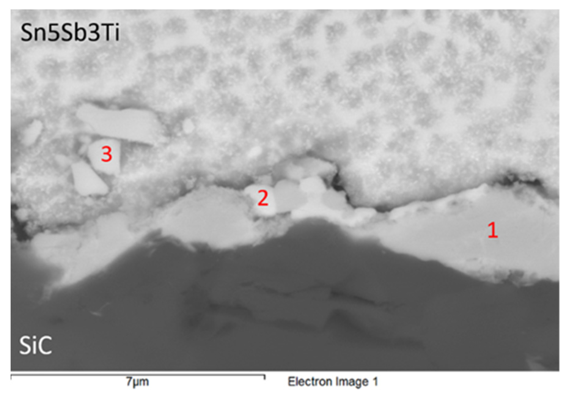
Figure 18.
Representation of measuring points on the SiC/Sn5Sb3Ti interface.
Figure 18.
Representation of measuring points on the SiC/Sn5Sb3Ti interface.
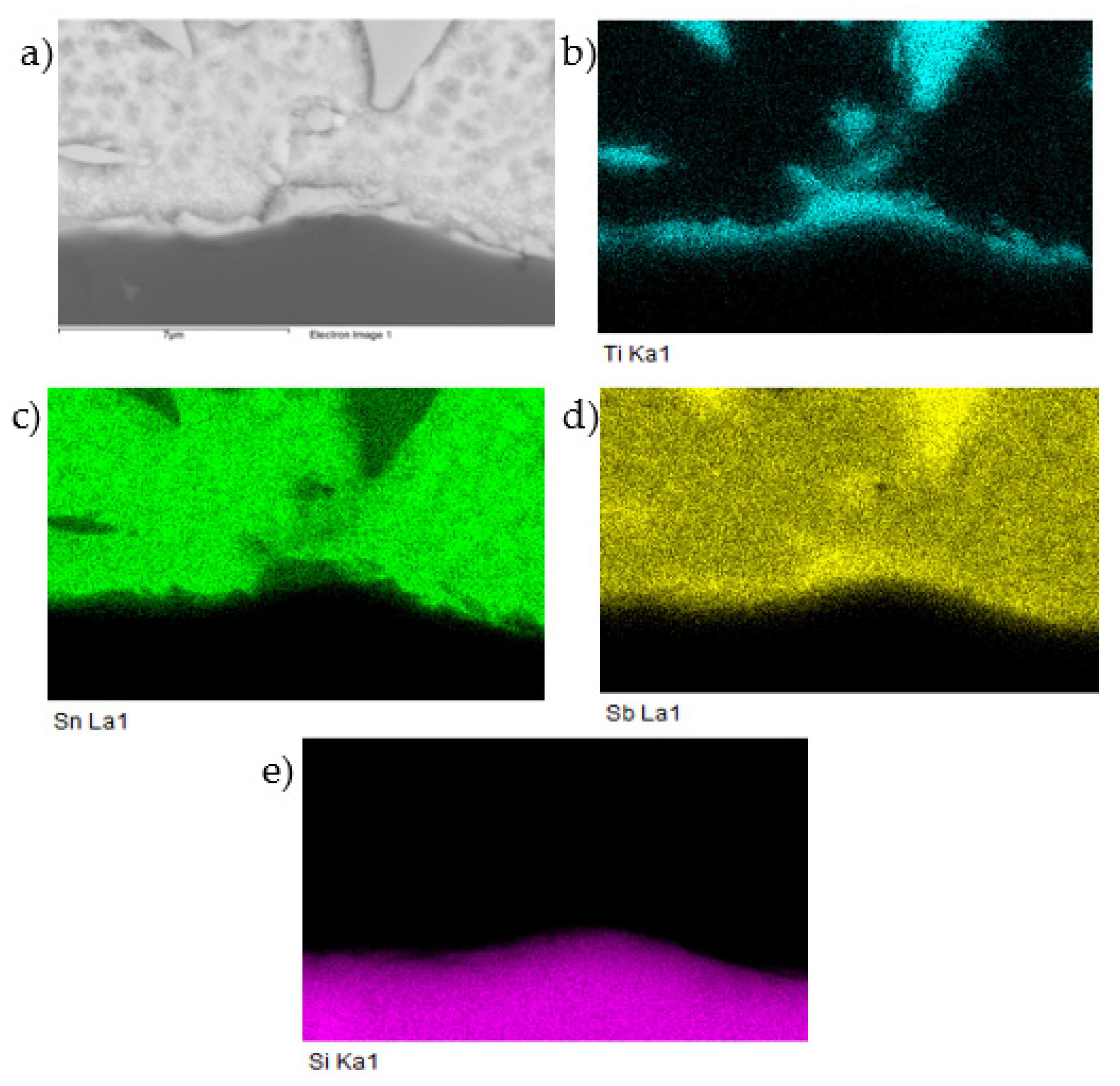
Figure 19.
Planar distribution of Ti, Sn, Sb, and Si elements in the boundary of the SiC/Sn5Sb3Ti joint; SEM photo of (a) the boundary, (b) Ti, (c) Sn, (d) Sb, and (e) Si.
Figure 19.
Planar distribution of Ti, Sn, Sb, and Si elements in the boundary of the SiC/Sn5Sb3Ti joint; SEM photo of (a) the boundary, (b) Ti, (c) Sn, (d) Sb, and (e) Si.
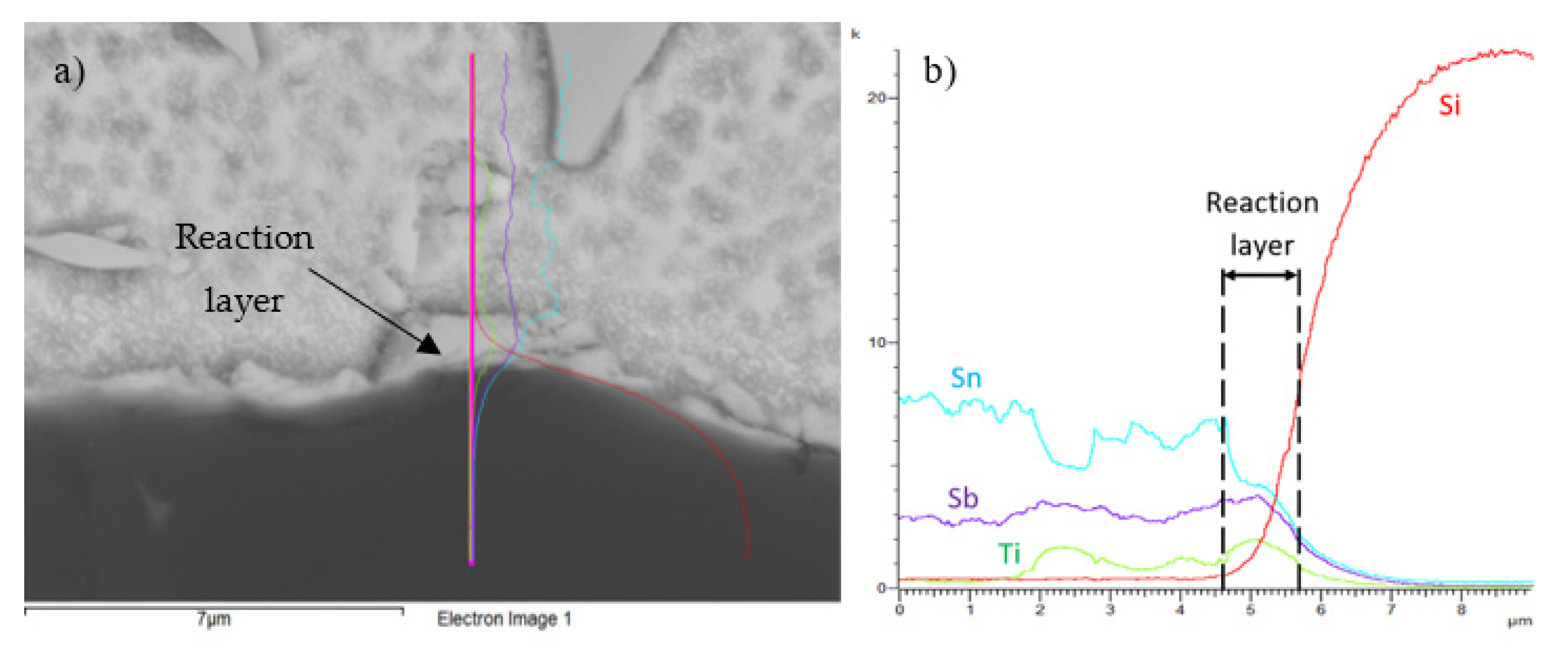
Figure 20.
Line EDX analysis of the SiC/Sn5Sb3Ti joint; (a) transition zone with a marked line; (b) concentration profiles of Sb, Sn, Ti, and Si elements.
Figure 20.
Line EDX analysis of the SiC/Sn5Sb3Ti joint; (a) transition zone with a marked line; (b) concentration profiles of Sb, Sn, Ti, and Si elements.
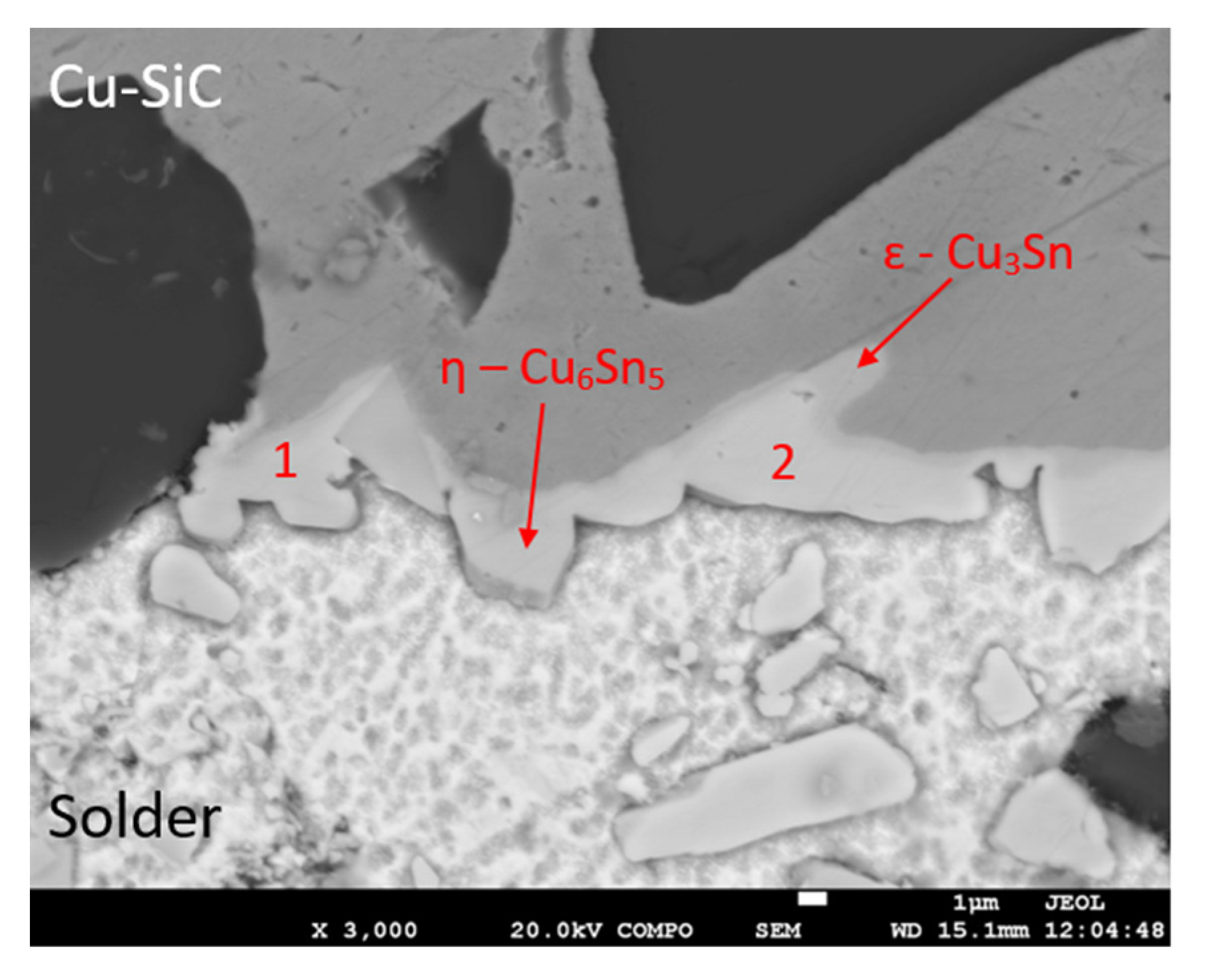
Figure 21.
Representation of the boundary in the Cu–SiC/Sn5Sb3Ti joint.
Figure 21.
Representation of the boundary in the Cu–SiC/Sn5Sb3Ti joint.
Figure 22.
Map of elements in the boundary of the Cu–SiC/Sn5Sb3Ti joint; SEM photo of (a) the boundary, (b) Cu, (c) Sn, (d) Sb, and (e) Ti.
Figure 22.
Map of elements in the boundary of the Cu–SiC/Sn5Sb3Ti joint; SEM photo of (a) the boundary, (b) Cu, (c) Sn, (d) Sb, and (e) Ti.
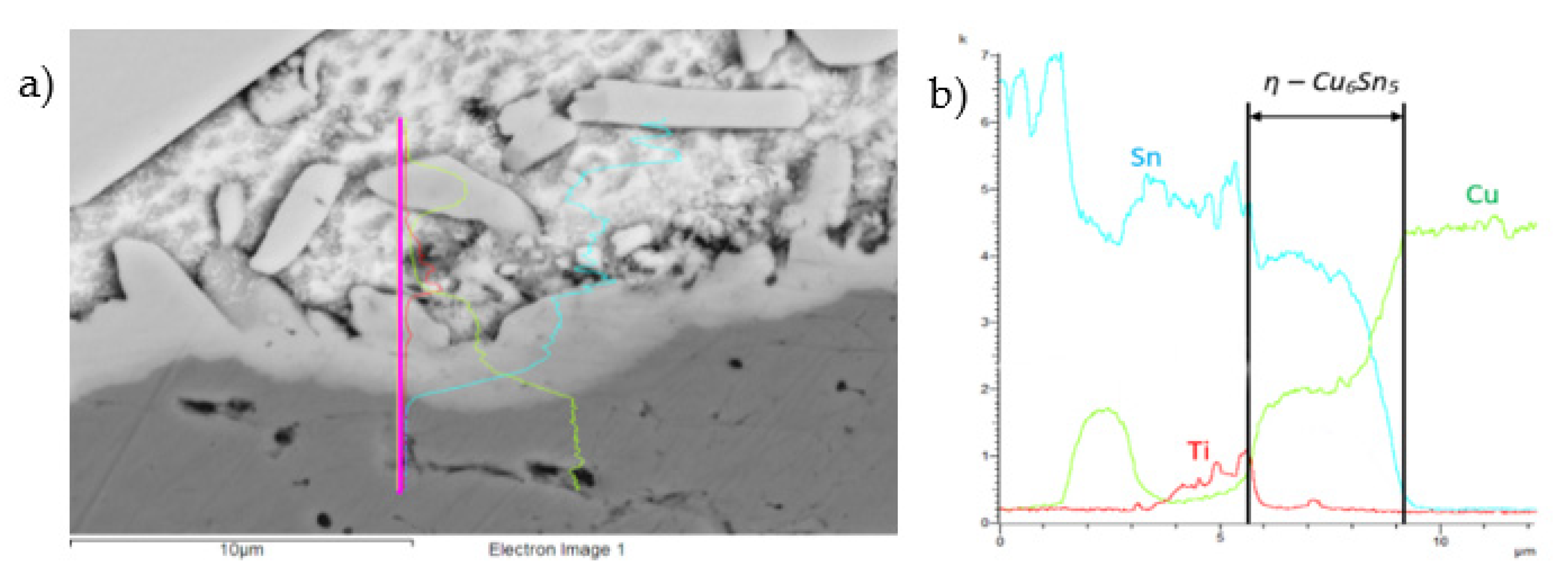
Figure 23.
The line EDX analysis of the Cu–SiC/Sn5Sb3Ti joint; (a) transition zone with a marked line; (b) concentration profiles of Sn, Sb, Ti, and Cu elements.
Figure 23.
The line EDX analysis of the Cu–SiC/Sn5Sb3Ti joint; (a) transition zone with a marked line; (b) concentration profiles of Sn, Sb, Ti, and Cu elements.
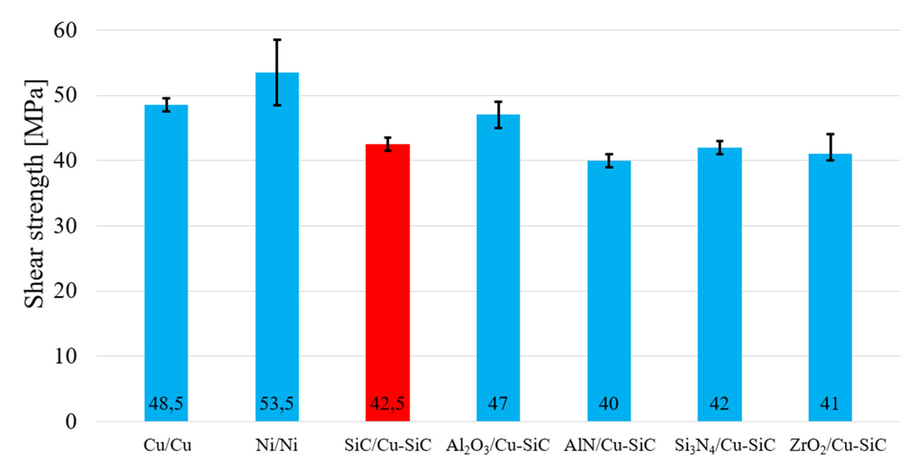
Figure 24.
Shear strength of soldered joints fabricated with the Sn5Sb3Ti solder.
Figure 24.
Shear strength of soldered joints fabricated with the Sn5Sb3Ti solder.
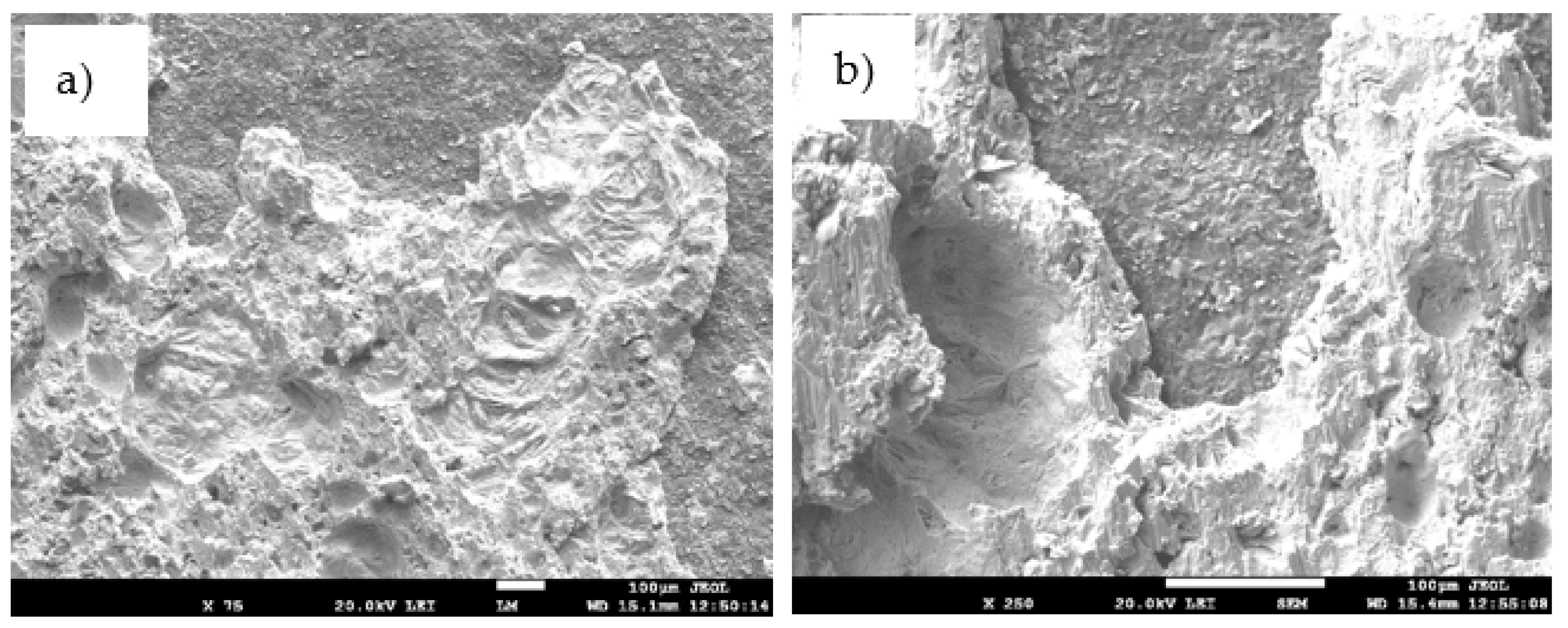
Figure 25.
The fractured surface of the soldered joint of SiC/Sn5Sb3Ti/CuSiC; (a) magnification 75×; (b) magnification 250×.
Figure 25.
The fractured surface of the soldered joint of SiC/Sn5Sb3Ti/CuSiC; (a) magnification 75×; (b) magnification 250×.
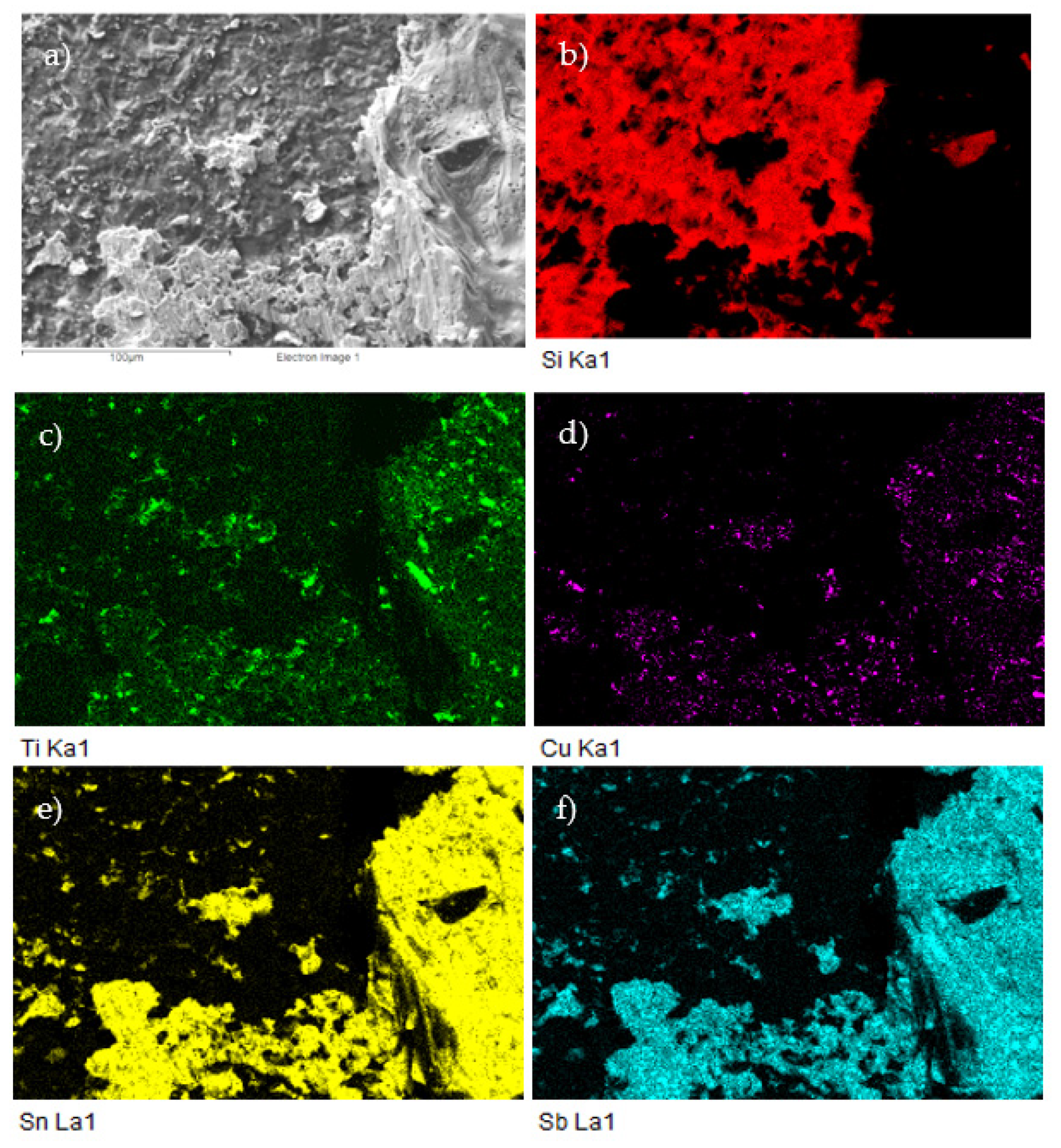
Figure 26.
The fractured surface of the soldered joint of SiC/Sn5Sb3Ti/Cu–SiC and the planar distribution of individual elements; (a) fracture morphology; (b) Si; (c) Ti; (d) Cu; (e) Sn; (f) Sb.
Figure 26.
The fractured surface of the soldered joint of SiC/Sn5Sb3Ti/Cu–SiC and the planar distribution of individual elements; (a) fracture morphology; (b) Si; (c) Ti; (d) Cu; (e) Sn; (f) Sb.
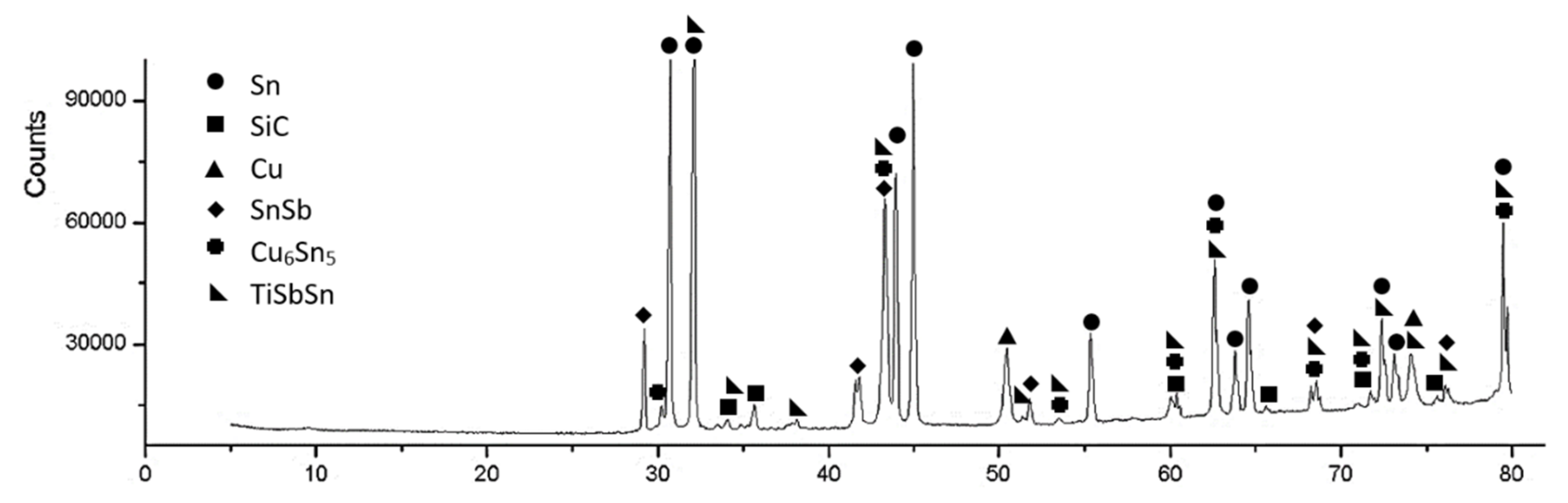
Figure 27.
XRD analysis of the boundary in the SiC/Sn5Sb3Ti/CuSiC joint.
Figure 27.
XRD analysis of the boundary in the SiC/Sn5Sb3Ti/CuSiC joint.
Table 1.
Composition of the Sn–Sb–Ti alloy and the results of chemical analysis by the ICP-AES method (wt.%).
Table 1.
Composition of the Sn–Sb–Ti alloy and the results of chemical analysis by the ICP-AES method (wt.%).
| Specimen | Charge (wt.%) | ICP-AES (wt.%) |
|---|
| Sn | Sb | Ti | Sn | Sb | Ti |
|---|
| Sn5Sb1Ti | 94.0 | 5.0 | 1.0 | Balance | 4.98 ± 0.15 | 1.21 ± 0.25 |
| Sn5Sb2Ti | 93.0 | 5.0 | 2.0 | Balance | 3.94 ± 0.48 | 1.79 ± 0.10 |
| Sn5Sb3Ti | 92.0 | 5.0 | 3.0 | Balance | 5.18 ± 0.26 | 3.31 ± 0.34 |
Table 2.
Ultrasonic soldering parameters.
Table 2.
Ultrasonic soldering parameters.
| Ultrasound power | 400 | (W) |
| Working frequency | 40 | (kHz) |
| Amplitude | 2 | (μm) |
| Soldering temperature | 260 | (°C) |
| Time of ultrasound activation | 5 | (s) |
Table 3.
The values of phase transformation in Sn5SbXTi solders measured by DTA analysis.
Table 3.
The values of phase transformation in Sn5SbXTi solders measured by DTA analysis.
| Composition | Onset Point on Heating (°C) | Onset Point on Cooling Down (°C) |
|---|
| | First measurement | Second measurement | First measurement | Second measurement |
| Sn5Sb1Ti | 247.5 | 242.2 | 239.6 | 239.6 |
| Sn5Sb2Ti | 241.8 | 234.0 | 230.7 | 230.9 |
| Sn5Sb3Ti | 234.9 | 233.9 | 228.6 | 228.3 |
Table 4.
HV microhardness of individual components of the Sn5Sb3Ti solder.
Table 4.
HV microhardness of individual components of the Sn5Sb3Ti solder.
| | Sn Matrix | Bright-Gray TiSbSn Phase | Dark-Gray Ti6(Sb,Sn)5 Phase |
|---|
| HV 0.01 | 20 | 174 | 939 |
Table 5.
EDX analysis of the Sn5Sb3Ti solder.
Table 5.
EDX analysis of the Sn5Sb3Ti solder.
| Spectrum | Sn (wt.%) | Sb (wt.%) | Ti (wt.%) | Solder Component |
|---|
| Spectrum 1 | 32.5 | 31.7 | 35.8 | Ti6(Sb,Sn)5 phase |
| Spectrum 2 | 33.9 | 30.9 | 35.2 | Ti6(Sb,Sn)5 phase |
| Spectrum 3 | 49.6 | 34.0 | 16.5 | TiSbSn phase |
| Spectrum 4 | 50.8 | 32.8 | 16.4 | TiSbSn phase |
| Spectrum 5 | 98.1 | 1.9 | 0 | Sn + Sb3Sn2 phase |
| Spectrum 6 | 97.0 | 3.0 | 0 | Sn + Sb3Sn2 phase |
Table 6.
Point EDX analysis of the SiC/SnSb5Ti3/Cu–SiC joint.
Table 6.
Point EDX analysis of the SiC/SnSb5Ti3/Cu–SiC joint.
| Spectrum | Sn (wt.%) | Sb (wt.%) | Ti (wt.%) | Solder Component |
|---|
| Spectrum 1 | 34.7 | 30.0 | 35.4 | Ti6(Sb,Sn)5 phase |
| Spectrum 2 | 34.6 | 30.1 | 35.3 | Ti6(Sb,Sn)5 phase |
| Spectrum 3 | 47.4 | 35.7 | 16.9 | TiSbSn phase |
| Spectrum 4 | 46.9 | 36.8 | 16.4 | TiSbSn phase |
| Spectrum 5 | 98.5 | 1.5 | 0 | Sn + Sb3Sn2 phase |
Table 7.
Point EDX analysis of the boundary in the SiC/Sn5Sb3Ti joint.
Table 7.
Point EDX analysis of the boundary in the SiC/Sn5Sb3Ti joint.
| Spectrum | Sn (wt.%) | Sb (wt.%) | Ti (wt.%) | Si (wt. %) | Solder Component |
|---|
| Spectrum 1 | 33.60 | 29.99 | 33.38 | 3.03 | (Ti,Si)6(Sb,Sn)5 phase |
| Spectrum 2 | 63.07 | 12.16 | 17.55 | 7.21 | Si7Ti10(Sb,Sn)17 phase |
| Spectrum 3 | 61.76 | 22.81 | 14.69 | 0.74 | TiSbSn phase |
Table 8.
Point EDX analysis of the boundary in the Cu–SiC/Sn5Sb3Ti joint.
Table 8.
Point EDX analysis of the boundary in the Cu–SiC/Sn5Sb3Ti joint.
| Spectrum | Sn (wt.%) | Cu (wt.%) | Solder Component |
|---|
| Spectrum 1 | 39.7 | 60.3 | η-Cu6Sn5 |
| Spectrum 2 | 39.1 | 61.0 | η-Cu6Sn5 |


