Article

Investigations of Structural and Electrical Properties of ALD Films Formed with the Ozone Precursor

by
Aleksandra Seweryn
1,*,
Krystyna Lawniczak-Jablonska
1,
Piotr Kuzmiuk
1,
Sylwia Gieraltowska
1,
Marek Godlewski
1 and
Robert Mroczynski
2
1
Institute of Physics, Polish Academy of Sciences, Aleja Lotnikow 32/46, PL-02668 Warsaw, Poland
2
Institute of Microelectronics and Optoelectronics, Warsaw University of Technology, Koszykowa 75, PL-00662 Warsaw, Poland
*
Author to whom correspondence should be addressed.
Materials 2021, 14(18), 5395; https://doi.org/10.3390/ma14185395
Submission received: 20 August 2021 / Revised: 12 September 2021 / Accepted: 14 September 2021 / Published: 18 September 2021
(This article belongs to the Special Issue Trends in Electronic and Optoelectronic Materials)

Abstract

:
The continuous development of ALD thin films demands ongoing improvements and changes toward fabricating materials with tailored properties that are suitable for different practical applications. Ozone has been recently established as a precursor, with distinct advantages over the alternative oxidizing precursors in the ALDs of advanced dielectric films. This study reports alumina (Al2O3) and hafnia (HfO2) formation using an O3 source and compares the obtained structural and electrical properties. The performed structural examinations of ozone-based materials proved homogenous high-k films with less vacancy levels compared to water-based films. The enhanced structural properties also result in the problematic incorporation of different dopants through the bulk layer. Furthermore, analysis of electrical characteristics of the MIS structures with ALD gate dielectrics demonstrated the improved quality and good insulating properties of ozone-based films. However, further optimization of the ALD technique with ozone is needed as a relatively low relative permittivity characterizes the ultra-thin films.

1. Introduction

Over the last two decades, atomic layer deposition (ALD) has been widely used in research and industry as an ideal technology for thin-film fabrication. ALD has a variety of advantages over conventional chemical vapor deposition (CVD) processes. Due to the unique self-limiting surface chemical reactions, ALD enables precise control of the thickness, composition, and stoichiometry of a grown material that is challenging to achieve via CVD methods [1,2]. Another essential advantage of ALD processing is its relatively low growth temperature, ranging from a typical 100 °C up to 350 °C. This feature makes ALD suitable for use in electronic and photonic devices based on transparent and flexible substrates, including polymers or hybrid structures with organic or low-dimensional materials [3,4,5]. Furthermore, ALD is commonly used for the fabrication of high-k dielectrics, transparent conductive oxides (TCOs), or conductive materials as gate-dielectrics in metal-oxide-semiconductor (MOS) devices [6,7], materials for non-volatile memory (NVSM) structures [8,9], optical coatings in lasers or light-emitting devices (LEDs) [10,11], membranes [12], sensing devices [13], waveguides [14], or photovoltaics [15,16].
The formation of thin films using ALD requires a precursor, efficiently supplying chemical reactions at the surface with reactive oxygen. Typical precursors that satisfy this requirement include oxygen (O2), hydrogen peroxide (H2O2), water (H2O), or ozone (O3), but water is most commonly used as the oxygen source during the fabrication of thin films. However, there are several reports that water-based ALD materials suffer from specific failures. It has been demonstrated that several films can delaminate from the substrate after elevated temperature treatment, and the substitution of water with ozone can limit such an effect [17,18].The growth of ozone-based materials can also be performed at significantly lower temperatures [19].
Furthermore, the improved quality of ALD materials has been shown to result in a significant smoothness level, lower leakage currents, and minor flat-band shift [20]. Ozone is characterized by a high electrochemical potential and high volatility. These two features are used in shortening purge times between ALD cycles and result in cost-savings [21]. The absence of hydrogen in the ozone molecule also reduces the risk of hydrogen and hydroxyl contamination in the deposited film.
Although the ALD method has been known for many years, and the first reports were from the 1970s [22,23], this method is still developing, which guarantees progress in thin films nanotechnology. In the case of oxide layers, the choice of the oxygen precursor can determine the properties of the layers. As we have already shown [24], the change from commonly used water to ozone significantly influenced, for example, the crystallography of ZnO layers. Selected metal precursors do not react with water due to the low activation energy. However, synthesis with ozone results in excellent film quality [25]. To systematize this issue after successful tests with dimethylzinc, experiments with another metal precursor were performed to examine if the properties of dielectric high-k oxide growth at low temperatures can be improved. In addition, to work with ALD ozone as a new oxygen precursor, the ALD procedures of high-k oxide growth using low temperatures, but with water, were developed [5].
In this work, we report the successful fabrication of alumina (Al2O3) and hafnia (HfO2) using an O3 source and compare the obtained structural and electrical properties of films. In the first stage of this study, we compare the structural and electrical parameters of Al2O3-based materials fabricated with water and ozone. Then, the selected processes were employed to fabricate alumina and hafnia layers with different thicknesses using an O3 oxygen source. The crystal structure, surface roughness, and chemical composition of fabricated films were analyzed. Moreover, the fabricated films were used as gate dielectric materials in MIS structures. Capacitance-voltage (C-V) and current-voltage (I-V) characteristics were examined to extract basic electrical parameters of investigated films. Our research study leads to the fabrication of good quality high-k films with properties suitable for electronic and photovoltaic applications.

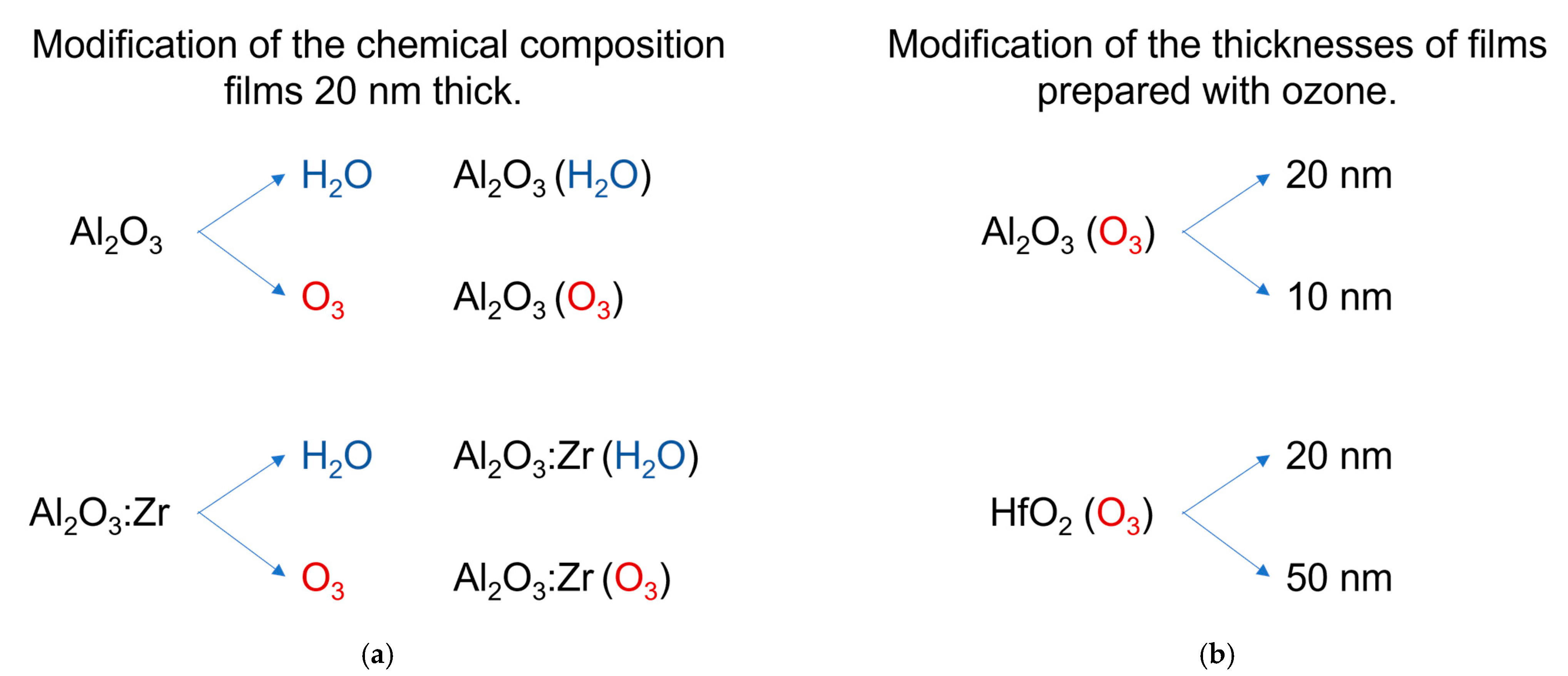
2. Materials and Methods

2.1. ALD of High-k Oxides

ALD technology consists of the sequential deposition of metal and oxide monolayers, which result in the growth of oxide films. To grow alumina and hafnia thin films, we used the Savannah-100 Cambridge NanoTech Inc., Cambridge, Massachusetts, USA ALD reactor with access to the purging gas—nitrogen, with the purity of 6.0. This reactor was equipped with a Savannah Ozone Generator with access to oxygen with a purity of 5.0, as reported in [24]. According to the manufacturer’s data, the used ozone generator was characterized by ~120 mg/L (~7.5 wt.% O3) capacity. We performed the growth of films at low temperatures, i.e., 100 °C and 90 °C for alumina and hafnia deposition, respectively. As metal precursors, we used the following compounds: trimethylaluminum (CAS Number: 75-24-1, Sigma Aldrich, Saint Louis, MO, USA), tetrakis(dimethylamido)hafnium(IV) (CAS Number: 19782-68-4, Sigma Aldrich, Saint Louis, MO, USA) for the growth of films, and tetrakis(dimethylamido)zirconium(IV) (CAS Number: 19756-04-8, Sigma Aldrich, Saint Louis, MO, USA) as dopant compounds for the preparation of the alumina film with the zirconium ions. According to the type of films, the used oxidants were deionized water (Millipore Milli-Q) or ozone received from the generator mentioned above. As previously reported, all processes were performed under vacuum, below 0.5 Torr [24,26]. Several ALD cycles were optimized to deposition of 10 nm and 20 nm films thick in the case of alumina and 20 nm and 50 nm films thick in the case of hafnia. Moreover, the modification of films was done by selecting oxygen precursors and through doping of Zr ions. In Figure 1, all types of investigated samples are summarized. The growth rate by ozone-based ALD processes is comparable to that with water-based oxygen precursors. To obtain 20 nm thick Al2O3 film with water 128 ALD cycles are needed up to 150 ALD cycles to get 20 nm thick Al2O3 film with water. This gives a growth rate of 1.6 Å/cycle and 1.3 Å/cycle for alumina water and ozone-based ALD appropriately. The result obtained for Al2O3:Zr were 1.5 Å/cycle and 1.2 Å/cycle with water and with ozone, respectively. The growth rate using hafnia ALD growth with the ozone was 1.4 Å/cycle.

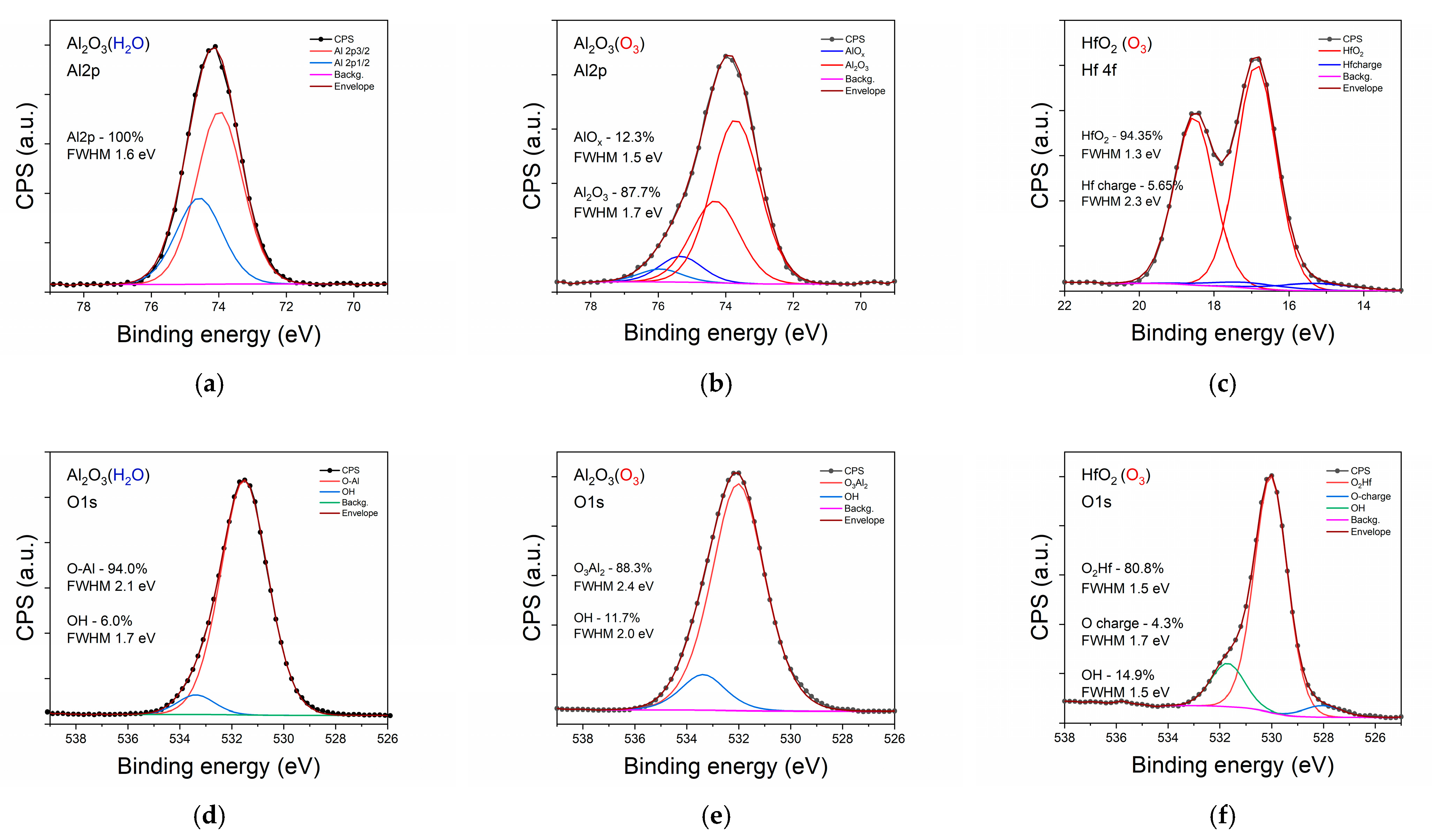
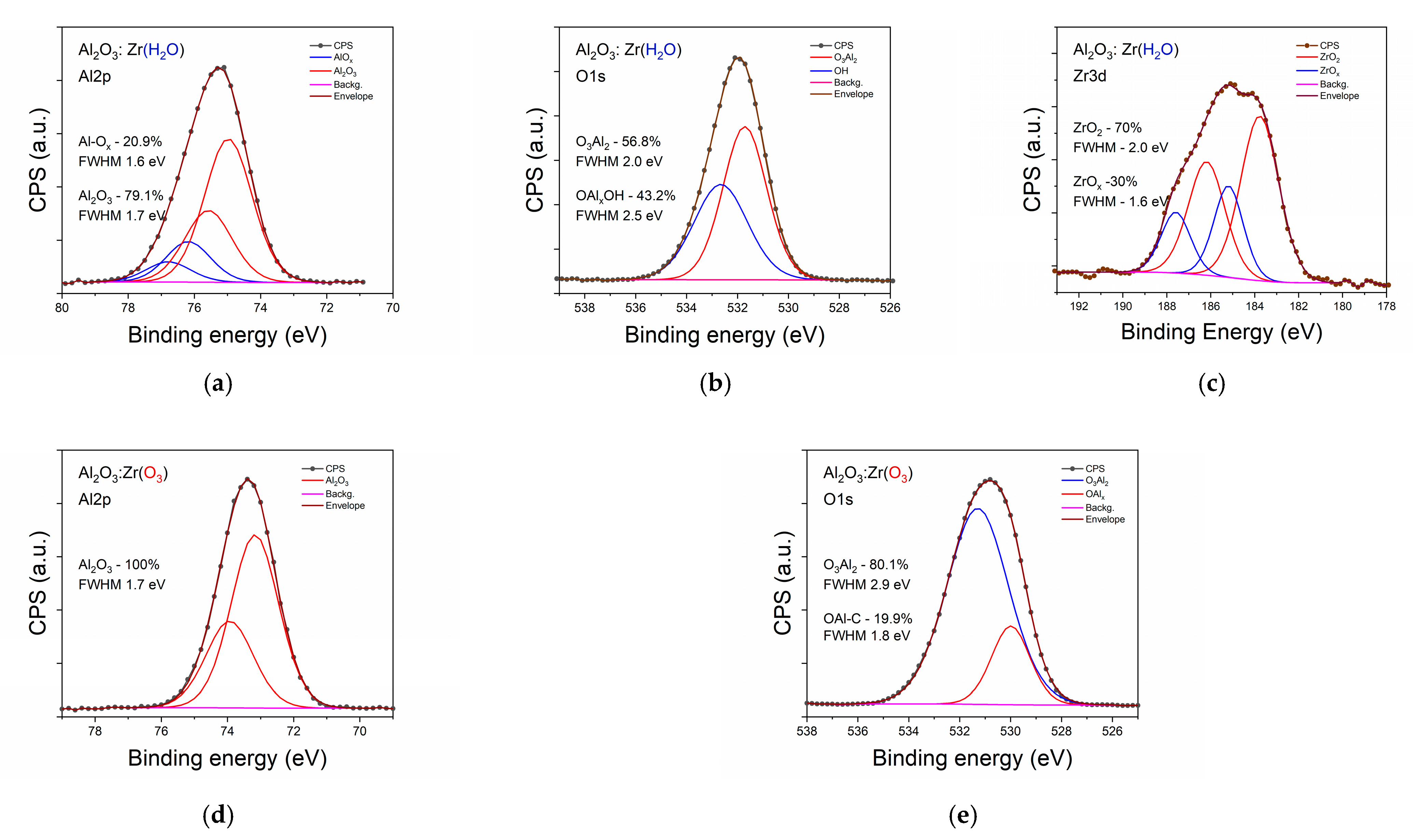
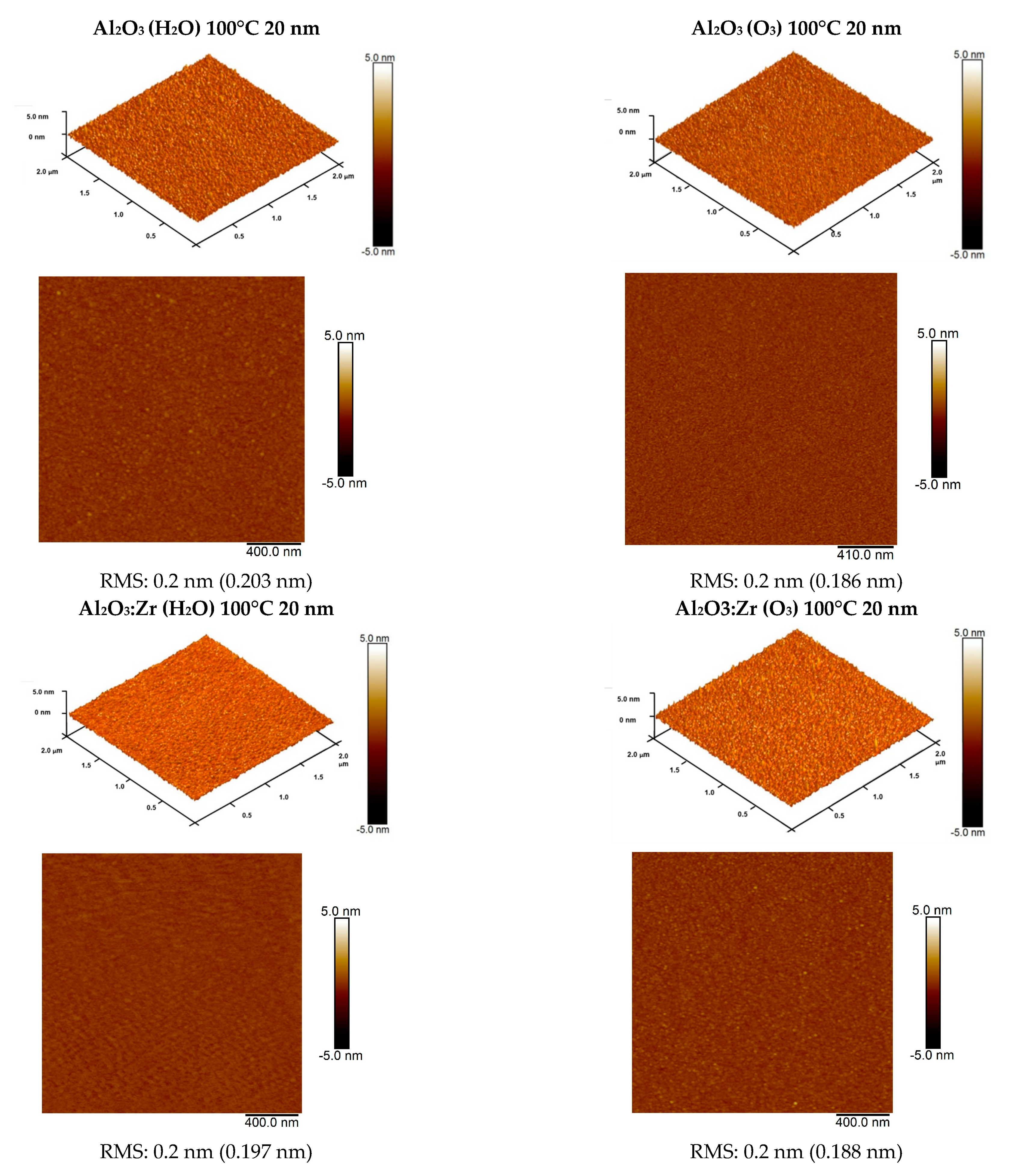
2.2. Structural Characterization of Dielectric Films

In order to describe the chemical composition and structural properties of films, selected measurements were performed. The film thicknesses were defined using a NanoCalc 2000-UV/VIS (Micropack GmbH, Ostfildern, Germany) with pre-installed software(Nanocalc232, Ostfildern, Germany).
XPS measurements were performed with a Scienta (Uppsala, Sweden) R4000 hemispherical analyzer (pass energy 200 eV) and monochromatic Al Kα (1486.7 eV) excitation (Scienta MX-650) working with a power of 150 W. The full width at half maximum (FWHM) of the 4f7/2 Au line measured under the same experimental conditions was 0.64 eV. The energy scale was calibrated, setting the C 1s line at the position of 285.0 eV. Samples were measured as received. A significant amount of C was detected on the sample surface. To gain information about the content of C in the bulk of the sample, short sputtering with an Ar+ ion gun at 1 kV, 5 mA, was performed. The spectra were analyzed using the commercial CASA XPS software package (Casa Software Ltd., version 2.3.17) with the Shirley background. The spectra were fitted with a mixed Gaussian–Lorentzian (GL (30)) function.
The surface morphology was investigated using atomic force microscopy (AFM, Bruker Dimension Icon, Santa Barbara, CA, USA) using PeakForce Tapping and silicon nitride probes with sharp tips (tip radius—2 nm). The surface roughness was determined by a root mean square (RMS) roughness of the AFM height measurements from images taken from a 10 × 10 μm2 region. The surface morphology of the layer was measured on silicon substrates.

2.3. MIS Structures Fabrication and Electrical Characterization

To perform electrical characterization of examined high-k films, MIS capacitors with Al2O3 or HfO2 gate dielectric layer were fabricated. In this study, silicon (Si) n-type substrates with a resistivity of 1 ÷ 10 Ωcm and an orientation (100) were used. The processing sequence of the MIS structures was as follows: Si substrates were cleaned employing a modified RCA (Radio Corporation of America) method (Piranha + SC1 + SC2 + HF dipping). Then, ALD processes, according to the procedure described in Section 2.1 were performed. After forming ALD oxides, the aluminum (Al) contact pads were developed through the standard UV (@400 nm) photolithography process and wet etching of excess aluminum. A pulsed-DC magnetron sputtering process was used to fabricate conductive films [27]. A PlasmaLab Oxford System 400 (Bristol, UK) was used to perform Al deposition on the top and bottom contacts. The fabricated MIS structures with the gate area of A = 1.7 × 10⁻⁴ cm2 allowed for determining the investigated structures’ basic electrical properties. The quality of obtained MOS structures was examined with a Keithley 4200 semiconductor characterization system (Tektronix, Beaverton, OR, USA) equipped with SUSS PM-8 probe station utilizing current–voltage (I-V) and capacitance–voltage (C-V) characteristic analyses. The procedure of the extraction of electrical parameters of the examined MIS structures was described in [28].

3. Results and Discussion

3.1. Structural Characterization of Investigated Samples

The uniform and homogenous ALD hafnia and alumina films were obtained on the Si substrate. First, the growth rates were estimated by performing ALD processes to define the number of ALD cycles needed. The thickness of the layers was in the range of 20–22 nm. This confirms the repeatability and scalability of the ALD measurement, which is one of the main advantages of this technology. The amorphous nature of the structures grown at low temperature has been shown in previous work [5].
Table 1 presents elements content (in at %) in investigated samples derived from XPS measurements of C 1s, O 1s, Al 2p, Hf 4f and Zr 3d lines.
Considering the content of the component in the investigated samples from the data presented in Table 1, is clearly seen that only the bulk of the HfO2 sample is stoichiometric, but, at the surface of this sample, an excess of oxygen was detected together with a high content of C. Opposite to this, in the case of Al2O3 samples, a deficit of oxygen was found in all samples besides that of Al2O3:Zr (O3). The growth performed in the presence of ozone reduced the number of oxygen defects in the Al2O3 (Al/O = 0.70 compared to 0.77 in the case of Al2O3 (H2O)) but prevented the incorporation of Zr. This suggests that Zr diffused through the oxygen vacancies during sample growth. The oxygen vacancies at the level of 0.77 were naturally present in the crystalline sapphire and significantly affected the chemistry of N incorporation from the nitrogen plasma [29]. The presence of O vacancies was necessary for the incorporation of N. Moreover, the increase in the number of O vacancies by forming the Al(NOy)x in the amorphous AlOx films significantly increased the amount of incorporated N. To check this hypothesis, an analysis of chemical states of the measured high-resolution spectra was performed. The results are presented in Figure 2 and Figure 3. For clarity of presentation, only the data for the bulk of the samples is shown. Examining the Al 2p spin-orbital in two cases (Al2O3 (H2O) and Al2O3:Zr (O3)), single chemical binding of Al was detected at the surface (not shown) and in the bulk of the samples with slightly better chemical order in the first sample (full width at half maximum (FWHM) 1.6 eV and 1.7 eV, respectively).
Nevertheless, the oxygen 1s orbitals for these samples had different components, indicating the different chemistry of oxygen incorporation. In the case of Al2O3 (H2O) 94% of the oxygen had binding energy (BE) for sapphire (Figure 2d). Other atoms were shifted more than 1.5 eV to higher energy, typical for absorbed water or other contamination [30]. For the Al2O3:Zr (O3) sample, two oxygen components provided a good envelope for a measured line, but the second component that took 20% of O had a BE lower by 1.3 eV compared with the fraction banded in sapphire. Moreover, the mainline was much broader (FWHM 2.9 eV) than in Al2O3 (H2O) (FWHM 2.1 eV). This low BE fraction consisted at the surface of more than 50% of the oxygen. This kind of fraction was not observed in the case of Al2O3 (O3) without Zr doping. In addition, Zr atoms, neither in bulk nor at the surface of Al2O3:Zr (O3), were detected. This may suggest that the low energy oxygen fraction filed the oxygen vacancies in the Al2O3 crystalline structure and formed higher valency component [31] and blocked Zr incorporation.
Analyzing the chemistry observed in the Al2O3:Zr (H2O) sample, where Zr was detected, at a level of 1.3 at % at the surface and 2.2 at % in bulk, we can clearly distinguish two fractions of Al and Zr as well at the surface, as in bulk. This fact demonstrates the presence of the fraction of Al atoms with a distorted atomic order compared to that in crystalline sapphire. At the surface, it is about 42% Al atoms and in bulk 21%, indicating that the process begins at the surface and advances to the bulk of the film. The second component has a higher BE, which is usually connected with fewer oxygen atom bonds to metal (e.g., [32] for MnO2 BE of Mn(IV) is 641.4 eV but fir MnO 641.1 eV Mn(II)) and a higher ionic state. In the case of Zr at the surface, only 50% of all Zr atoms have atomic order as in ZrO2 while 70% do in bulk. Two components of the O 1s line provide good fitting, one with BE for sapphire and a high BE component evidencing other kinds of oxygen bindings. High energy components at the surface consist of almost 79% O. Still, in bulk, only 43% is much broader than the sapphire component, which usually shows several different atoms surrounding in this fraction.
Two kinds of Al bonds were also detected in the case of the Al2O3 (O3) sample, confirming the lack of oxygen, but the second higher BE fraction was at the level of 10% (20% in the case of the Al2O3:Zr (H2O) sample). The second fraction of oxygen was also much smaller in the Al2O3 (O3) sample. For HfO2 (O3), the one fraction of Hf 4f was used to fit the spectra and two typical components for O 1s (Figure 2c, f), but a small charging effect was observed at the low energy site of both spectra.
Summing up, XPS studies showed that films grown in the presence of ozone have fever oxygen vacancies than those grown in the presence of H2O, but this prevents the accommodation of dopants.
Since the low roughness of the surface is a crucial parameter for the electrical properties of the films, AFM measurements were performed. The data are presented below. Figure 4 and Figure 5 indicate a very flat surface for low-temperature thin films grown using ALD with a thickness of approximately 20 nm. The extremely low surface roughness with an RMS roughness value of about 0.2 nm was achieved for all aluminum oxide layers, including Al2O3 and Al2O3 with Zr obtained at 100 °C from water or ozone as the oxide precursor. It can also be clearly noticed that a slightly better surface morphology can characterize high-k films fabricated using O3. HfO2 layers deposited at 90 °C are characterized by a somewhat higher surface roughness, but are still very homogenous, with an RMS roughness level of about 0.4 nm.
The processes of ALD deposition for the HfO2 and Al2O3 layers were investigated by the authors [5,33]. The Hf and Al precursors used by us in the present paper are the same—tetrakis(dimethylamido)hafnium (TDMAH) and trimethylaluminum (TMA), respectively—as in our previous studies. The oxygen precursor used in previous experiments was deionized water:
Hf [(CH3)2N]4 + 2H2O → HfO2 + 4HN(CH3)2
2Al(CH3)3 + 3H2O → Al2O3 + 6CH4
where ozone is used in the present paper. We determined the so-called ALD growth window from earlier studies. We established that the ALD window for HfO2 is in the range of 130 °C to 140 °C, giving the growth rate of 1.4 Å per cycle, and, for Al2O3, from 180 °C to 200 °C, giving a growth rate of 1.0 Å per cycle. However, both films can be deposited at lower temperatures. At 80 °C, the growth rate for Al2O3 drops slightly to 0.8 Å per cycle [33]. A reverse effect was observed for HfO2, i.e., the growth rate was even higher, about 1.5 Å per cycle [33]. For HfO2, we observed that films with a thickness above about 200 nm showed a tendency to crystallize, even at low process temperatures. For Al2O3 layers, this tendency is weaker (as we concluded from XRD investigations) [33], but is still a lower growth temperature and thinner films are more suitable for microelectronic applications. This is because the amorphous structure is expected to have substantially reduced leakage current. Higher leakage currents are associated with the presence of grain boundaries appearing in crystalline films [2]. We also observed that films grown at a lower temperature are very smooth. From the AFM studies, we concluded that the surface roughness’s root mean square (RMS) value depends on the growth temperature and the layer thickness. It was the lowest (RMS = 0.2 nm) for the thin Al2O3 films (50 nm) and a growth temperature of 100°C [33]. Based on the results discussed above, we selected a low growth temperature for both Al2O3 and HfO2 layers but changed the source of oxygen from deionized water to ozone. From initial studies, we checked that such changes affected the material properties and may affect hydrogen and carbon concentrations in the films and film stoichiometry. Regarding film stoichiometry, since ozone is more reactive, we expected that the concentration of vacancies in the films might be affected.

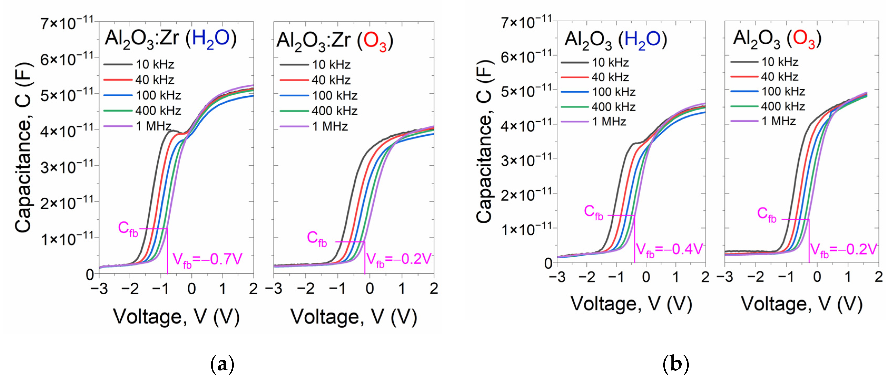
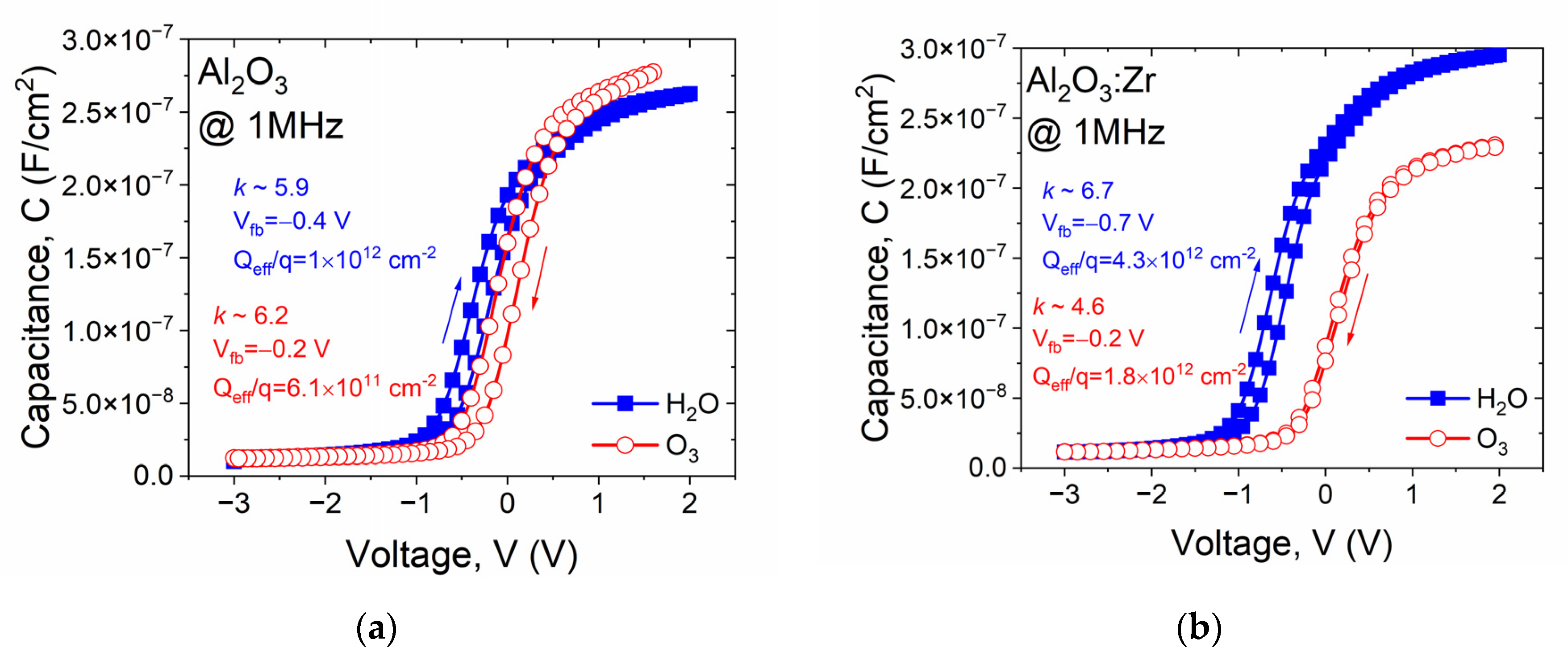
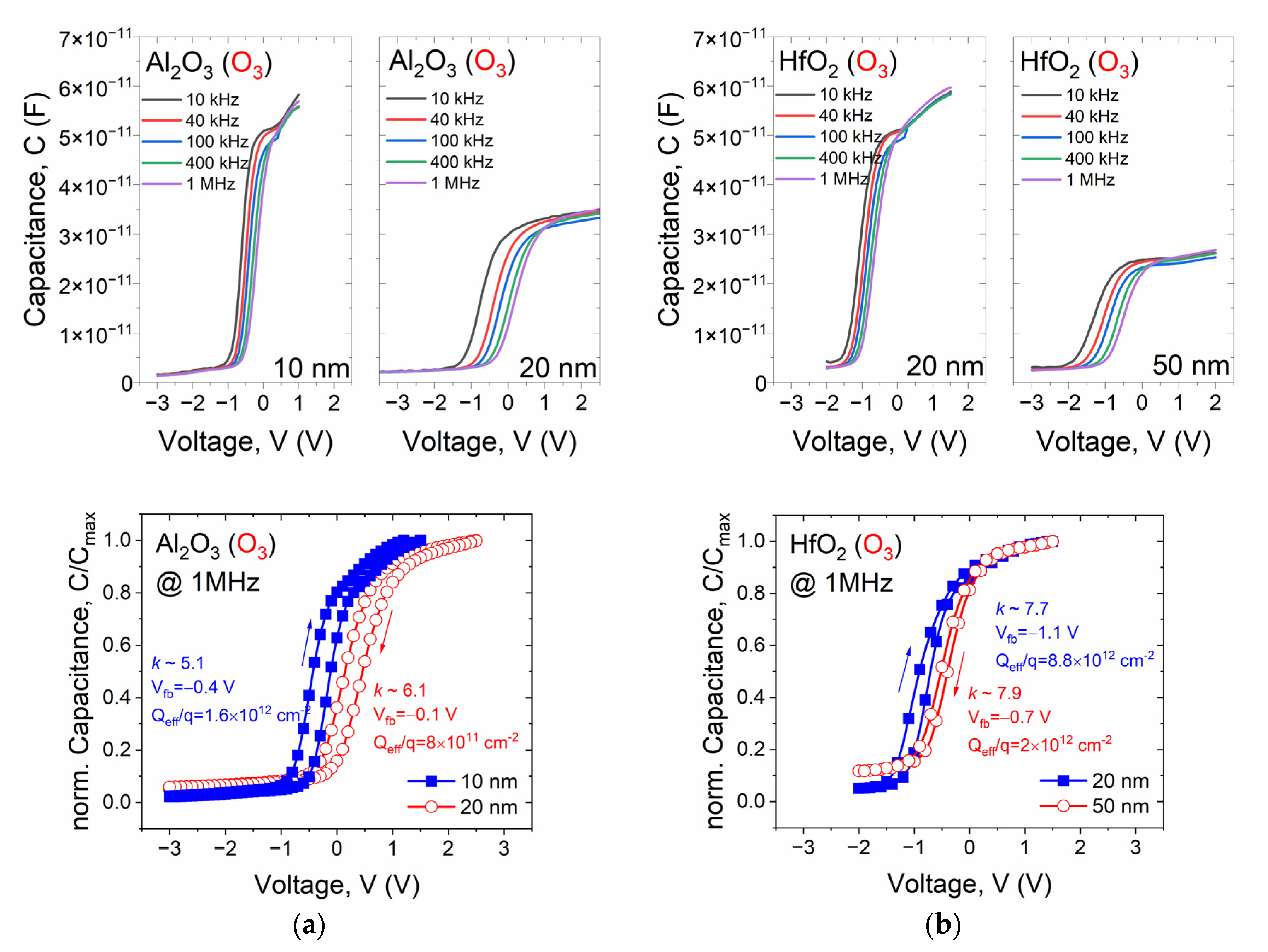
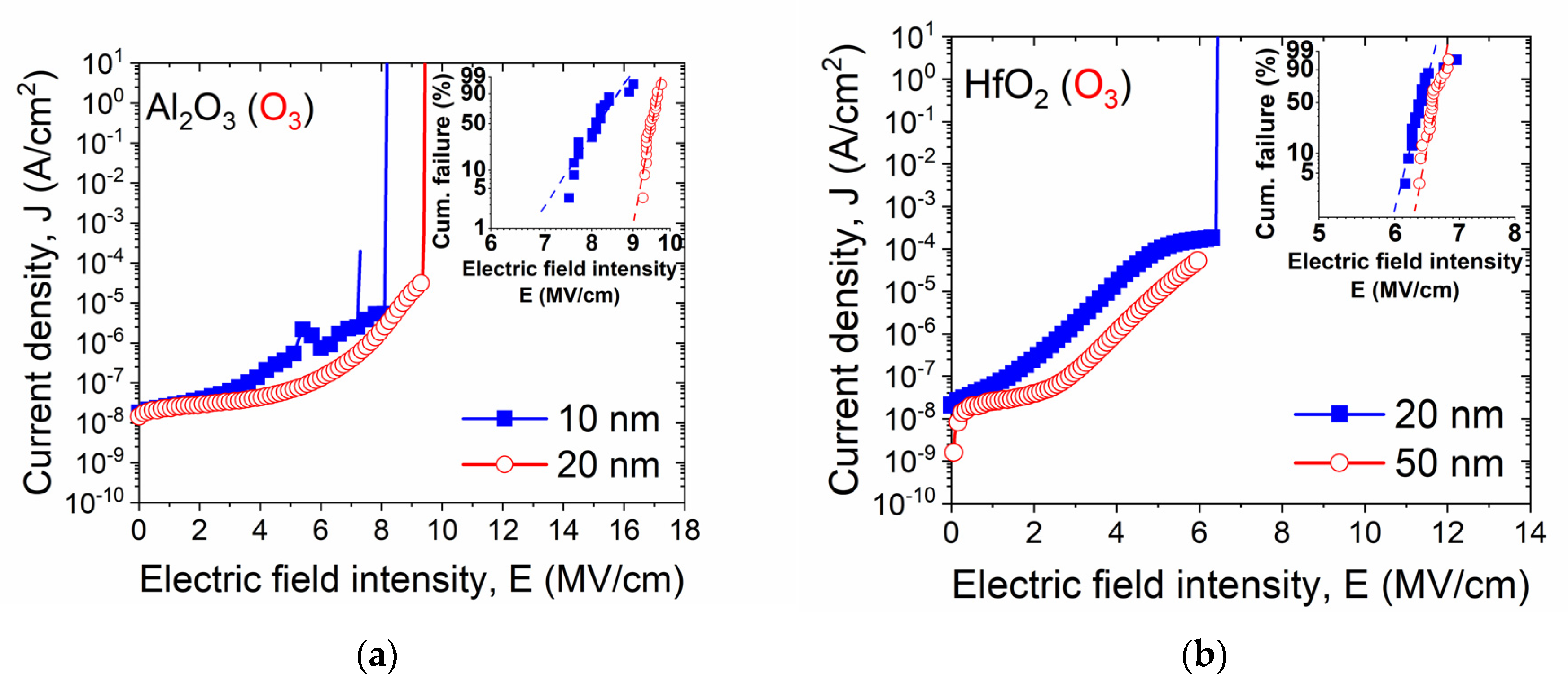
3.2. Electrical Characterization of MIS Structures with ALD Films as Gate-Dielectric Layers

The analysis of electrical parameters of high-k films was started with a comparison of MIS structures with Al2O3-based gate dielectrics fabricated using H2O and O3 precursors. At first, MIS devices with 20 nm Al2O3 and Al2O3:Zr films were fabricated. In Figure 6, a comparison of the family of C-V characteristics of MIS capacitors is presented.
It is worth noting that the C-V characteristics of the structures with Al2O3-based materials using H2O can be characterized using a characteristic “knee” in the depletion regime of silicon. The magnitude of this effect is more prominent as the signal frequency becomes lower. This implicates the presence of charge traps in the dielectric film, i.e., shallow traps that keep up with the signal frequency. This effect does not occur in ozone-based films, suggesting a more effective saturation of dangling bonds during the ALD process employing the O3. Moreover, the flat-band (Vfb) voltage values of the C-Vs of MIS devices with ozone-based films are smaller (in absolute values) than in ALD films fabricated with a water precursor. This is related to the generation of a positive charge in the dielectric layer bulk [34]. One of the possible mechanisms of the positive charge formation is the generation of hole trap sites induced by broken bonds at the semiconductor/dielectric charge traps that are significantly large. Thus, the dielectric quality of high-k films fabricated with O3 is improved, which was further verified by comparing C-Vs interfaces. These traps are formed during the growth of a dielectric film. As the ozone precursor is more chemically reactant than water, water-based dielectric films (@1MHz) are depicted in Figure 7.
The results presented in Figure 7 confirm that Al2O3 fabricated with an ozone precursor is characterized by a higher relative permittivity, lower Vfb (in absolute values), and lower effective charge (Qeff/q) compared to a material formed using H2O precursor. The magnitude of a hysteresis loop is comparable for both films. The comparison of C-Vs of MIS devices with Al2O3:Zr films also revealed better electrical parameters for the high-k film formed with O3, which manifests in a similar improvement of dielectric quality material, even with the disappearance of the C-V hysteresis loop. However, a relatively lower relative permittivity was obtained, i.e., 6.7 and 4.6 for H2O-based, and O3-based ALD film, respectively.
MIS structures with the ALD Al2O3 and HfO2 O3-based layers with different thicknesses were fabricated in the next step. In the case of aluminum oxide, 10 nm- and 20 nm-thick materials have been deposited, while in the case of hafnium oxide—20 nm and 50 nm. In Figure 8, a comparison of the families of C-V characteristics of the examined materials is presented. Moreover, the magnitude of hysteresis loops of both types of MIS stacks is also depicted. As the different thicknesses characterize the considered materials, the depicted C-Vs are constructed as normalized capacitance levels to each stack’s maximum capacitance.
After analyzing the data presented in Figure 8, it can be concluded that the frequency dispersion is smaller than in thicker oxides in both cases for the MIS devices with thinner dielectric films. The presence of charge traps in the depletion region also becomes more noticeable, which is not observed in the case of investigated capacitors with thicker Al2O3 and HfO2 films. Furthermore, a slightly higher permittivity and lower Vfb values (in absolute values) have been demonstrated in both thicker films. These findings are further confirmed by a lower effective charge density, as shown in Figure 8.
It can also be noticed that a typically higher permittivity value and slightly higher Qeff/q values characterize the obtained hafnium oxide films compared to Al2O3. The latter observation may result from the fact that an inhomogeneous interfacial layer (IL) between the semiconductor and the hafnia film may have formed, which is a typical effect for hafnium-based dielectric material deposition on silicon [35]. It has already been shown that, due to the chemical instability of the hafnium oxide films, oxygen atoms easily diffuse towards the semiconductor/dielectric interface. Thus, a very thin IL is formed which deteriorates, not only the properties of the MIS stack, but also reduces the permittivity value of the dielectric film. Simultaneously, the flow of oxygen atoms from the dielectric layer bulk results in a deterioration of the stoichiometry of HfOx film. The latter also contributes to lowering the electrical quality of the investigated dielectric stack.
Considering the insulating properties of ALD materials, the measured current–voltage (I-V) characteristics of fabricated MIS devices have been compared and expressed as gate leakage current density vs. electric field intensity (Figure 7). The presented data in Figure 9 compare the leakage current density of MIS stacks with investigated ALD films. As the inset, a cumulative failure analysis is depicted as Weibull plots. Around twenty MIS capacitors with each gate dielectric material were examined to introduce the statistical data of the distribution of breakdown voltage values.
The analyzed I-V characteristics of MIS devices with each type of O3-based ALD material showed very similar insulating properties in this study. However, a slightly lower leakage current density was observed for thicker ALD films, resulting from improved electrical properties described during C-Vs analysis. For Al2O3 films, up to ~6 MV/cm, a relatively low leakage current density, was demonstrated, i.e., between 10−8 and 10−7 A/cm2. Then, the leakage current increased and the breakdown occurred between 7 and 8 MV/cm, and 9 MV/cm, for thinner and thicker Al2O3 film, respectively. Similar results can be found in [36,37]. For instance, in [36], depending on the temperature of the ALD process, the breakdown phenomenon was observed at 7.0 and 6.3 MV/cm for Al2O3 deposited at room temperature and annealed at 400 °C, respectively. A significantly lower breakdown voltage value, i.e., 5.3 MV/cm, for a MIS stack with Al2O3 deposited at 177 °C was demonstrated in [37].
In the case of a MIS structure with a HfO2 film, the leakage current density is within the range of 10−8 and 10−7 A/cm2 up to 2 MV/cm, and then starts to increase, and the breakdown occurs at a relatively high electric field intensity, between 6 and 7 MV/cm. It is worth noting that for both investigated thicker high-k films, the distribution of breakdown voltage values is very narrow, i.e., around 90% of structures fail within the range of 0.5 MV/cm.
The results in the present work show very good electrical properties of the films grown with ozone. For example, for Al2O3 films, up to ~6 MV/cm leakage current density is between 10−8 and 10−7 A/cm2. Similar values are obtained for HfO2 films. A leakage current must be as small as 10–7 A/cm2 at 1 V for applications in non-volatile memories [38,39,40]. In addition, we examined if the small amount of Zr in Al2O3 films will increase the chance of use of Al2O3 application in Si-based microelectronics. Considering the required properties of alternative oxides to replace SiO2 as a gate [35,41,42], Al2O3 films are best but were not used since the dielectric constant is too low. This may be changed by introducing some amount of Zr, since the dielectric constant of ZrO2 is similar to that of HfO2. The first results presented in this study are encouraging and makes the investigated ozone-based ALD materials very promising for future practical applications. The dielectric materials studied in this work can be characterized by suitable electrical parameters for most applications in MOS/MIS semiconductor devices and other structures where dielectric material electrical performance is crucial. However, the obtained relatively lower permittivity noted that the deposition processes need further studies and optimization for MIS structures and devices applications. The considerably lower k-values compared to those commonly found in the literature may be due to the lower density of the obtained films and/or the interfacial layer and quantum mechanical effects [43]. As the results presented in this work prove the relatively high density of deposited films, we believe that the lower permittivity values can be attributed to the presence of IL film and the deteriorated interfacial properties reported in this work. The presence of an interfacial dielectric layer adds an extra capacitor in series with a high-k film that lowers the calculated permittivity value. The additional IL is formed from a silicon oxide (SiOx) material with a permittivity value of ~3.9 or lower. Simultaneously, non-stoichiometric IL also deteriorates the MIS stack’s electrical properties, as shown in the present work. Thus, optimizing ALD technology and finding the best growth parameters are of importance for the future.

4. Conclusions

The structural and electrical properties of ALD alumina and hafnia thin films have been investigated. The high-k materials were fabricated using water and ozone as the oxygen precursors. All films were homogenous with low RMS values, as AFM showed. The films grown with ozone are characterized by a smaller amount of oxygen vacancies compared to those grown with water, but this prevents the accommodation of dopants. The present study also indicated that an ozone oxygen precursor is superior to a water one, resulting in films with better electrical parameters. Such films show a low hysteresis of C-V characteristics, higher breakdown voltages, and lower leakage current, which is important for MIS structure applications. However, the technology still needs optimization and further investigations to fully understand the chemical reactions that occur during the growth of the high-k film towards improving the relative permittivity value.

Author Contributions

Conceptualization and idea of this study, A.S. and R.M.; structural measurements and analysis of results, A.S., S.G., K.L.-J., P.K.; electrical characterization and data analysis, R.M.; writing—original draft preparation, A.S., K.L.-J. and R.M.; writing—review and editing, A.S. and R.M.; visualization, A.S. and R.M.; supervision, M.G. and R.M.; project administration, R.M.; funding acquisition, R.M. All authors have read and agreed to the published version of the manuscript.

Funding

This work has been partly supported by The National Centre for Research and Development (NCBiR) under grant No. TECHMATSTRATEG1/347012/3/NCBR/2017 (HYPERMAT) in the course of “Novel technologies of advanced materials—TECHMATSTRATEG” and by Materials Technologies project granted by Warsaw University of Technology under the program Excellence Initiative: Research University (ID-UB) entitled “Graphene as an indicator of the conditions of dielectric films technology on semiconductor substrates”.

Institutional Review Board Statement

Not applicable.

Informed Consent Statement

Not applicable.

Conflicts of Interest

The authors declare no conflict of interest.

References

  1. Crowell, J.E. Chemical methods of thin film deposition: Chemical vapor deposition, atomic layer deposition, and related technologies. J. Vac. Sci. Technol. A 2003, 21, S88–S95. [Google Scholar] [CrossRef]
  2. Mallick, B.C.; Hsieh, C.-T.; Yin, K.-M.; Gandomi, Y.A.; Huang, K.-T. Review—On Atomic Layer Deposition: Current Progress and Future Challenges. ECS J. Solid State Sci. Technol. 2019, 8, N55–N78. [Google Scholar] [CrossRef]
  3. Biercuk, M.; Monsma, D.J.; Marcus, C.M.; Becker, J.S.; Gordon, R.G. Low-temperature atomic-layer-deposition lift-off method for microelectronic and nanoelectronic applications. Appl. Phys. Lett. 2003, 83, 2405–2407. [Google Scholar] [CrossRef] [Green Version]
  4. Oviroh, P.O.; Akbarzadeh, R.; Pan, D.; Coetzee, R.A.M.; Jen, T.-C. New development of atomic layer deposition: Processes, methods and applications. Sci. Technol. Adv. Mater. 2019, 20, 465–496. [Google Scholar] [CrossRef] [Green Version]
  5. Gieraltowska, S.; Wachnicki, L.; Witkowski, B.S.; Mroczynski, R.; Dluzewski, P.; Godlewski, M. Characterization of dielectric layers grown at low temperature by atomic layer deposition. Thin Solid Film. 2015, 577, 97–102. [Google Scholar] [CrossRef]
  6. Choi, J.; Mao, Y.; Chang, J. Development of hafnium based high-k materials—A review. Mater. Sci. Eng. R Rep. 2011, 72, 97–136. [Google Scholar] [CrossRef]
  7. Bethge, O.; Abermann, S.; Henkel, C.; Bertagnolli, E. Low temperature atomic layer deposition of high-k dielectric stacks for scaled metal-oxide-semiconductor devices. Thin Solid Film. 2009, 517, 5543–5547. [Google Scholar] [CrossRef]
  8. Maikap, S.; Lee, H.Y.; Wang, T.-Y.; Tzeng, P.-J.; Wang, C.C.; Lee, L.S.; Liu, K.C.; Yang, J.-R.; Tsai, M.-J. Charge trapping characteristics of atomic-layer-deposited HfO2 films with Al2O3 as a blocking oxide for high-density non-volatile memory device applications. Semicond. Sci. Technol. 2007, 22, 884–889. [Google Scholar] [CrossRef] [Green Version]
  9. Mroczyński, R.; Taube, A.; Gieraltowska, S.; Guziewicz, E.; Godlewski, M. Application of deposited by ALD HfO2 and Al2O3 layers in double-gate dielectric stacks for non-volatile semiconductor memory (NVSM) devices. Appl. Surf. Sci. 2012, 258, 8366–8370. [Google Scholar] [CrossRef]
  10. Leskelä, M.; Mattinen, M.; Ritala, M. Review Article: Atomic layer deposition of optoelectronic materials. J. Vac. Sci. Technol. B 2019, 37, 030801. [Google Scholar] [CrossRef] [Green Version]
  11. Mangote, B.; Gallais, L.; Zerrad, M.; Commandré, M.; Gao, L.H.; LeMarchand, F.; Lequime, M.; Melninkaitis, A.; Mirauskas, J.; Sirutkaitis, V.; et al. Study of the laser matter interaction in the femtosecond regime: Application to the analysis of the laser damage of optical thin films. SPIE Opt. Syst. Des. 2011, 8168, 816815. [Google Scholar] [CrossRef]
  12. Weber, M.; Julbe, A.; Ayral, A.; Miele, P.; Bechelany, M. Atomic Layer Deposition for Membranes: Basics, Challenges, and Opportunities. Chem. Mater. 2018, 30, 7368–7390. [Google Scholar] [CrossRef]
  13. Heikkinen, I.T.; Repo, P.; Vähänissi, V.; Pasanen, T.; Malinen, V.; Savin, H. Efficient surface passivation of black silicon using spatial atomic layer deposition. Energy Procedia 2017, 124, 282–287. [Google Scholar] [CrossRef]
  14. Caballero-Espitia, D.; Lizarraga, E.; Borbon-Nuñez, H.; Contreras-Lopez, O.; Tiznado, H.; Marquez, H. Study of Al2O3 thin films by ALD using H2O and O3 as oxygen source for waveguide applications. Opt. Mater. 2020, 109, 110370. [Google Scholar] [CrossRef]
  15. Dullweber, T.; Schmidt, J. Industrial Silicon Solar Cells Applying the Passivated Emitter and Rear Cell (PERC) Concept—A Review. IEEE J. Photovolt. 2016, 6, 1366–1381. [Google Scholar] [CrossRef]
  16. Pietruszka, R.; Witkowski, B.; Zielony, E.; Gwóźdź, K.; Placzek-Popko, E.; Godlewski, M. ZnO/Si heterojunction solar cell fabricated by atomic layer deposition and hydrothermal methods. Sol. Energy 2017, 155, 1282–1288. [Google Scholar] [CrossRef]
  17. von Gastrow, G.; Li, S.; Repo, P.; Bao, Y.; Putkonen, M.; Savin, H. Ozone-based Batch Atomic Layer Deposited Al2O3 for Effective Surface Passivation. Energy Procedia 2013, 38, 890–894. [Google Scholar] [CrossRef]
  18. Lüdera, T.; Lauermann, T.; Zuschlag, A.; Hahn, G.; Terheiden, B. Al2O3/SiNx-Stacks at Increased Temperatures: Avoiding Blistering During Contact Firing. Energy Procedia 2012, 27, 426–431. [Google Scholar] [CrossRef] [Green Version]
  19. Muñoz-Rojas, D.; Maindron, T.; Esteve, A.; Piallat, F.; Kools, J.; Decams, J.-M. Speeding up the unique assets of atomic layer deposition. Mater. Today Chem. 2019, 12, 96–120. [Google Scholar] [CrossRef]
  20. Mahapatra, R.; Maikap, S.; Ray, S.K. Electrical properties of ultrathin HfO2 gate dielectrics on partially strain compensated SiGeC/Si heterostructures. J. Electroceramics 2006, 16, 545–548. [Google Scholar] [CrossRef]
  21. Kim, J.B.; Kwon, D.R.; Chakrabarti, K.; Lee, C.; Oh, K.Y.; Lee, J.H. Improvement in Al2O3 dielectric behavior by using ozone as an oxidant for the atomic layer deposition technique. J. Appl. Phys. 2002, 92, 6739–6742. [Google Scholar] [CrossRef]
  22. Antson, J. United States Patent (19). Geothermics 1977, 14, 595–599. [Google Scholar]
  23. Puurunen, R.L. A Short History of Atomic Layer Deposition: Tuomo Suntola’s Atomic Layer Epitaxy. Chem. Vap. Depos. 2014, 20, 332–344. [Google Scholar] [CrossRef] [Green Version]
  24. Seweryn, A.; Pietruszka, R.; Witkowski, B.S.; Wierzbicka, A.; Jakiela, R.; Sybilski, P.; Godlewski, M. Structural and electrical parameters of ZnO thin films grown by ALD with either water or ozone as oxygen precursors. Crystals 2019, 9, 16–19. [Google Scholar] [CrossRef] [Green Version]
  25. Miikkulainen, V.; Leskela, M.; Ritala, M.; Puurunen, R. Crystallinity of inorganic films grown by atomic layer deposition: Overview and general trends. J. Appl. Phys. 2013, 113, 021301. [Google Scholar] [CrossRef]
  26. Seweryn, A.; Pielok, A.; Lawniczak-Jablonska, K.; Pietruszka, R.; Marcinkowska, K.; Sikora, M.; Witkowski, B.S.; Godlewski, M.; Marycz, K.; Śmieszek, A. Zirconium Oxide Thin Films Obtained by Atomic Layer Deposition Technology Abolish the Anti-Osteogenic Effect Resulting from miR-21 Inhibition in the Pre-Osteoblastic MC3T3 Cell Line. Int. J. Nanomed. 2020, 15, 1595–1610. [Google Scholar] [CrossRef] [Green Version]
  27. Mroczyński, R.; Iwanicki, D.; Fetliński, B.; Ożga, M.; Świniarski, M.; Gertych, A.; Zdrojek, M.; Godlewski, M. Optimization of Ultra-Thin Pulsed-DC Magnetron Sputtered Aluminum Films for the Technology of Hyperbolic Metamaterials. Crystal 2020, 10, 384. [Google Scholar] [CrossRef]
  28. Belosludtsev, A.; Yakimov, Y.; Mroczyński, R.; Stanionytė, S.; Skapas, M.; Buinovskis, D.; Kyžas, N. Effect of Annealing on Optical, Mechanical, Electrical Properties and Structure of Scandium Oxide Films. Phys. Status Solidi A 2019, 216, 1–7. [Google Scholar] [CrossRef]
  29. Lawniczak-Jablonska, K.; Zytkiewicz, Z.R.; Gieraltowska, S.; Sobanska, M.; Kuzmiuk, P.; Klosek, K. Chemical bonding of nitrogen formed by nitridation of crystalline and amorphous aluminum oxide studied by X-ray photoelectron spectroscopy. RSC Adv. 2020, 10, 27932–27939. [Google Scholar] [CrossRef]
  30. Dupin, J.C.; Gonbeau, D.; Vinatier, P.; Levasseur, A. Systematic XPS studies of metal oxides, hydroxides and peroxides. Phys. Chem. Chem. Phys. 2000, 2, 1319–1324. [Google Scholar] [CrossRef]
  31. Wu, L.Q.; Li, Y.C.; Li, S.Q.; Li, Z.Z.; Tang, G.D.; Qi, W.H.; Xue, L.C.; Ge, X.S.; Ding, L.L. Method for estimating ionicities of oxides using O1s photoelectron spectra. AIP Adv. 2015, 5, 097210. [Google Scholar] [CrossRef]
  32. Crist, B.V. Handbooks of Monochromatic XPS Spectra; XPS International LLC.: Mountain View, CA, USA, 2005; Volume 2. [Google Scholar]
  33. Gieraltowska, S.; Sztenkiel, D.; Guziewicz, E.; Godlewski, M.; Łuka, G.; Witkowski, B.; Wachnicki, Ł.; Łusakowska, E.; Dietl, T.; Sawicki, M. Properties and Characterization of ALD Grown Dielectric Oxides for MIS Structures. Acta Phys. Pol. A 2011, 119, 692–695. [Google Scholar] [CrossRef]
  34. Mroczyński, R.; Beck, R.B. Reliability issues of double gate dielectric stacks based on hafnium dioxide (HfO2) layers for non-volatile semiconductor memory (NVSM) applications. Microelectron. Reliab. 2012, 52, 107–111. [Google Scholar] [CrossRef]
  35. Wilk, G.D.; Wallace, R.; Anthony, J.M. High-κ gate dielectrics: Current status and materials properties considerations. J. Appl. Phys. 2001, 89, 5243–5275. [Google Scholar] [CrossRef]
  36. Reklaitis, I.; Radiunas, E.; Malinauskas, T.; Stanionytė, S.; Juška, G.; Ritasalo, R.; Pilvi, T.; Taeger, S.; Strassburg, M.; Tomašiūnas, R. A comparative study on atomic layer deposited oxide film morphology and their electrical breakdown. Surf. Coat. Technol. 2020, 399, 126123. [Google Scholar] [CrossRef]
  37. Groner, M.; Elam, J.; Fabreguette, F.; George, S. Electrical characterization of thin Al2O3 films grown by atomic layer deposition on silicon and various metal substrates. Thin Solid Film. 2002, 413, 186–197. [Google Scholar] [CrossRef]
  38. Robertson, J. High dielectric constant gate oxides for metal oxide Si transistors. Rep. Prog. Phys. 2005, 69, 327–396. [Google Scholar] [CrossRef]
  39. Robertson, J. High dielectric constant oxides. Eur. Phys. J. Appl. Phys. 2004, 28, 265–291. [Google Scholar] [CrossRef] [Green Version]
  40. Lo, S.H.; Buchanan, D.A.; Taur, Y.; Wang, W. Quantum-mechanical modeling of electron tunneling current from the inversion layer of ultra-thin-oxide nMOSFET’s. IEEEE Electron Device Lett. 1997, 18, 209–211. [Google Scholar] [CrossRef]
  41. Houssa, M. High-k Gate Dielectrics; Institute of Physics Publishing: Bristol, UK, 2004. [Google Scholar]
  42. Hori, T. Gate Dielectrics and MOS ULSIs: Principles, Technologies, and Applications; Springer: Berlin, Germany, 1997. [Google Scholar]
  43. Natori, K.; Otani, D.; Sano, N. Thickness dependence of the effective dielectric constant in a thin film capacitor. Appl. Phys. Lett. 1998, 73, 632–634. [Google Scholar] [CrossRef] [Green Version]
Figure 1. List of the samples investigated in this work: (a) modification of the chemical composition of films, (b) modification of the thicknesses of films.
Materials 14 05395 g001
Figure 2. High-resolution spectra for metals and oxygen for investigated samples of pure Al2O3 and HfO2 as measured for bulk, after short Ar+ sputtering to remove surface contamination Al line: (ac), O line (df).
Materials 14 05395 g002
Figure 3. High-resolution spectra for metals and oxygen for investigated samples of pure Al2O3 doped with Zr ions as measured for bulk, after short Ar+ sputtering to remove surface contamination: with water (ac), with ozone (d,e).
Materials 14 05395 g003
Figure 4. AFM images (2 × 2 μm2) and RMS roughness values of Al2O3 and Al2O3:Zr thin films (~20 nm thick) grown with ALD from water (H2O) or ozone (O3) at 100 °C on Si substrate.
Materials 14 05395 g004
Figure 5. AFM images (2 × 2 μm2 and 10 × 10 μm2) and RMS roughness value of HfO2 thin films (20 nm thick) grown with ALD from ozone (O3) at 90 °C on Si substrate.
Materials 14 05395 g005
Figure 6. The typical family of high-frequency C-V characteristics of MIS structure with 20 nm ALD gate dielectric film investigated in this work: (a) Al2O3 and (b) Al2O3:Zr.
Materials 14 05395 g006
Figure 7. Comparison of the hysteresis loop of representative C-V characteristics (signal frequency, f = 1 MHz) of MIS structures with Al2O3-based gate dielectric layer: (a) Al2O3 and (b) Al2O3:Zr.
Materials 14 05395 g007
Figure 8. Comparison of representative high-frequency C-V characteristics of MIS structures with ALD gate dielectric films deposited with O3 precursor: (a) Al2O3 and (b) HfO2.
Materials 14 05395 g008
Figure 9. Comparison of representative I-V characteristics of MIS structures with ALD gate dielectric layers expressed as gate leakage current density vs. electric field intensity for (a) Al2O3 and (b) HfO2; Weibull plots of cumulative breakdown distribution vs. electric field intensity are also shown as insets.
Materials 14 05395 g009
Table 1. Elements content (in at %) in investigated samples from XPS measurements of C 1s, O 1s and Al 2p, Hf 4f and Zr 3d lines. “Surface” is related to sample measure as received, “bulk” to sample after sputtering with Ar+ ions with 1 kV energy.
SampleCsurfaceCbulkOsurfaceObulkAl(Hf)surfaceAl(Hf)bulkZrsurfaceZrbulk
Al2O3 (H2O) 14.24.948.553.737.3
Al/O = 0.77
41.4
Al/O = 0.77
Al2O3 (O3)20.54.846.854.932.7
Al/O = 0.70
40.3
Al/O = 0.73
Al2O3:Zr (H2O)18.64.546.852.733.3
Al/O = 0.71
40.6
Al/O = 0.77
1.32.2
Al2O3:Zr (O3)15.65.950.555.834.0
Al/O = 0.67
38.3
Al/O = 0.69
0
HfO2 (O3)33.94.546.063.720.1
Hf/O = 0.44
31.8
Hf/O = 0.5
Publisher’s Note: MDPI stays neutral with regard to jurisdictional claims in published maps and institutional affiliations.

