Article

Chemical Vapor Deposited Mixed Metal Halide Perovskite Thin Films

by
Siphesihle Siphamandla Magubane
1,*,
Christopher Joseph Arendse
1,*,
Siphelo Ngqoloda
1,
Franscious Cummings
1,
Christopher Mtshali
2 and
Amogelang Sylvester Bolokang
1,3
1
Department of Physics and Astronomy, University of the Western Cape, Private Bag X17, Bellville 7535, South Africa
2
iThemba LABS, National Research Foundation, Somerset West 7129, South Africa
3
CSIR Material Science & Manufacturing, Advanced Materials and Engineering, Meiring Naude Road, Pretoria 0001, South Africa
*
Authors to whom correspondence should be addressed.
Materials 2021, 14(13), 3526; https://doi.org/10.3390/ma14133526
Submission received: 11 May 2021 / Revised: 9 June 2021 / Accepted: 18 June 2021 / Published: 24 June 2021
(This article belongs to the Special Issue CVD Deposition and Characterization of Multilayers and Thin Films)

Abstract

:
In this article, we used a two-step chemical vapor deposition (CVD) method to synthesize methylammonium lead-tin triiodide perovskite films, MAPb1−xSnxI3, with x varying from 0 to 1. We successfully controlled the concentration of Sn in the perovskite films and used Rutherford backscattering spectroscopy (RBS) to quantify the composition of the precursor films for conversion into perovskite films. According to the RBS results, increasing the SnCl2 source amount in the reaction chamber translate into an increase in Sn concentration in the films. The crystal structure and the optical properties of perovskite films were examined by X-ray diffraction (XRD) and UV-Vis spectrometry. All the perovskite films depicted similar XRD patterns corresponding to a tetragonal structure with I4cm space group despite the precursor films having different crystal structures. The increasing concentration of Sn in the perovskite films linearly decreased the unit volume from about 988.4 Å3 for MAPbI3 to about 983.3 Å3 for MAPb0.39Sn0.61I3, which consequently influenced the optical properties of the films manifested by the decrease in energy bandgap (Eg) and an increase in the disorder in the band gap. The SEM micrographs depicted improvements in the grain size (0.3–1 µm) and surface coverage of the perovskite films compared with the precursor films.

1. Introduction

Three-dimensional (3-D) organo-lead halide perovskites, which form a perovskite structure of ABX3, have received tremendous research interest over the past decade [1]. As a result, we have seen tremendous progress in the solar cell (SC) performance from 3.8% to 25.5% power conversion efficiency (PCE) of these lead-based perovskite SCs. This is due to their high optical absorption coefficients, high charge carrier mobilities, long charge carrier diffusion lengths, low exciton binding energy, bandgap tunability, and low-temperature solution processability [2,3,4,5,6,7,8,9,10]. Despite this overwhelming development, considering the nature of the solar absorption spectrum, the maximum theoretical efficiency can be achieved in a single junction device with an optimum energy bandgap (Eg) of about 1.1 to 1.3 eV [11]. Broadening the range of solar absorption to the near-infrared (IR) region could further enhance the performance of perovskite SCs [12]. Therefore, the relatively wide Eg (1.5–2.2 eV) of organo-lead halide perovskite dramatically limits the sensitivity of the film in the IR region of the solar spectrum [13]. Another major drawback that is associated with lead-based perovskites is the toxicity of the lead (Pb) element and its compounds, which pose threats to the environment and human well-being, thus restricting the commercialization of Pb-based perovskite solar cells (PSCs) [7,14,15,16,17,18].
The challenges that are associated with Pb-based perovskites have sparked research interest in the partial and complete replacement of Pb with tin (Sn) in the perovskite structure, not only to reduce the toxic Pb but also to extend the absorption range to above 960 nm wavelengths, i.e., below 1.3 eV [19,20,21,22,23,24,25]. On one hand, a complete replacement of Pb seems to be improbable at this point due to the low PCE of Sn-based perovskite SCs that is driven by the rapid crystallization of Sn-based perovskite, making the film growth control to be a challenge [26,27,28]. Moreover, Sn-perovskite films are very unstable compared to pure Pb-based perovskites [24,25,27]. This instability is due to the easy oxidation of Sn2+ to Sn4+ that causes Sn vacancies in the film, thus promoting non-radiative recombination, which leads to reduced charge carrier lifetimes in the PSCs [29,30]. On the other hand, tremendous efficiency improvements and various discoveries have been made in the low-bandgap (1.17–1.1.38 eV) Pb-Sn PSCs [31,32,33,34].
The technique that is mostly employed to deposit the low-bandgap mixed Pb-Sn halide perovskite is one-step spin-coating with antisolvent treatment followed by annealing at about 100 °C for crystallization [31]. Different ratios of solvents, i.e., Dimethylformamide (DMF) and Dimethyl sulfoxide (DMSO), have been explored and different organic cations such as methylammonium (MA), formamidinium (FA), cesium (Cs), and halides like iodine (I), bromine (Br), chlorine (Cl), or a combination of these halides have been investigated [30,35,36,37,38,39,40,41,42,43]. It has been observed that uniform, large-grained, and pinhole-free films with high surface coverage are requirements for the high performance of Sn-based PSCs [31]. However, there seems to be a consensus that the control of crystal growth becomes complicated as the proportion of Sn increases in the perovskite structure [32,44,45]. The crystal structure of methylammonium lead-tin triiodide (MAPb1−xSnxI3) perovskites transition from tetragonal phase (space group 14cm) to pseudo-cubic phase (space group P4mm) when x nears 0.5 (for x ranging from 0 to 1) [31]. During this transition the valence band (VB) and the conduction band (CB) undergo an energy shift from −5.45 and −3.90 eV (for x = 0) to −4.73 and −3.63 eV (for x = 1), respectively [28,31,33,46,47,48]. These changes are attributed to the perovskite crystal lattice compression and distortion as a result of increased Sn incorporation [49,50,51,52].
Additional efforts, such as the incorporation of additives like halogens and thiocyanate (SCN) series in the perovskite structure, film surface passivation, and interface engineering aiming at reducing grain boundaries and charge scattering thereby extending the charge carrier lifetimes, and increasing the charge diffusion lengths, have all been explored. Halide doping, including Cl or Br, is another effective strategy to enhance the film quality of the mixed Pb-Sn perovskites [49,53]. This allows the precursor solution to convert to a perovskite consisting of intermixing of Br/Cl and iodine in the lattice, thereby reducing Sn and iodine vacancies in the film [49,53]. Other researchers have proved that similarly to halide doping, the addition of antioxidants and ascorbic acids such as tin fluoride (SnF2), tin sulfide (SnS), quaternary ammonium halide (Me4NBr), tetramethylammonium iodide (Me4NI), methylammonium bromide (MABr), lead thiocyanate (Pb(SCN)2), and other thiocyanate (SCN) salts can improve the perovskite film quality [31]. They ascribed this to reductive additives that do not only prevent Sn2+ oxidation, but also promote the crystallization growth through strong coordination between PbI2/SnI2 and an organic cation or a combination of organic cations which allows the complete interaction and conversion of metal halides into perovskite [53,54,55,56,57,58,59,60,61].
Attempts to improve the charge diffusion length, including but not limited to the incorporation of cadmium iodide (CdI) and/or metallic Sn in the low bandgap Pb-Sn perovskite, have also been explored [30,59,60]. This reduces the free hole concentration and electron density, which leads to an improved diffusion length of up to 3 μm [31]. Other attempts, such as the deposition of ultrathin bulk-heterojunction (BHJ) organic semiconductor layer as an intermediary between the hole transport layer (HTL) and the mixed low bandgap perovskite to minimize the energy loss by reducing energy level mismatch and passivating defects in the HTL/perovskite interface have been reported [58,61,62,63].
The need to produce stable perovskite films that will withstand exposure to outdoor conditions without introducing morphological and structural changes that consequently affect the electronic properties of the films, remains. This article, therefore, aims to optimize and establish the processing conditions to synthesize uniform and stable low bandgap mixed Pb-Sn perovskite films that exhibit homogenous elemental distribution using a chemical vapor deposition (CVD) technique. We have successfully controlled the concentration of Sn in the perovskite structure and then examined the structure-property relationship of these perovskite films in relation to the deposition technique. The technique is divided into two steps that include (i) the co-evaporation and deposition of tin chloride-lead iodide (SnCl2-PbI2) compound films, followed by (ii) the conversion of these compound films into perovskite through exposure to methylammonium iodide (MAI) vapor [64]. The two-step deposition technique is employed because it promises a better understanding of the formation mechanism of the perovskite films through controlling the precursor films deposition parameters and the conversion parameters, independently [62,63]. Also, the CVD method avoids the use of solvents to dissolve the precursor chemicals, which results in highly stable, uniform, largely grained, and pin-hole free perovskite films [62,63]. This is due to the low pressure (1 mbar) and inert environment in which the processing/deposition takes place. In terms of large-scale production and reproducibility, the CVD technique is the strongest contender over the cost-efficient solution-processed perovskites, because it is well established in the semiconductor industry especially in silicon-based research [64,65].

2. Materials and Methods

2.1. Precursor Thin Films Deposition

Mixed SnCl2-PbI2 precursor films were deposited on 1.5 × 2 cm2 corning glass substrates that were cleaned via sonication in boiling hellmanex solution and isopropanol for 15 min each in an ultrasonic bath. After that, the substrates were rinsed in boiling deionized (DI) water and then dried with a nitrogen (N2) gun. The deposition system that was used is composed of a horizontal quartz tube enclosed with the three-independent temperature-controlled zone furnace (Brother XD 1600MT Furnace Co., LTD, Zhengzhou, China) [64]. All the materials were purchased from Sigma Aldrich (St. Louis, MO, USA) and were used as obtained without any further purification. A ceramic boat containing a mixture of different powder amounts of 98% purity SnCl2 (i.e., 2.5, 5, 10, and 15 mg) and 20 mg of 99.9% PbI2 was placed in the 1st zone while the substrates were placed in the 2nd zone at about 16–20 cm away from the source boat [64]. The tube of the furnace was then sealed and pumped down to a base pressure of 0.04 mbar. Next, the tube was purged with N2 gas at a rate of 200 sccm (i.e., standard cubic centimeters per minute) to flush away all form of contaminations pre-existed in the tube. Then, the source boat was heated to a temperature of 380 °C while flowing N2 gas at a rate of 500 sccm to direct the vapor towards the substrates. The deposition pressure was between 2.5 to 3 mbar and the duration was set for 20 min, after which the sources were evaporated completely. For comparison purposes, pure PbI2 and SnCl2 films were deposited in a similar manner except that the evaporation temperature was 270 °C for the SnCl2 source and 380 °C for PbI2.

2.2. Precursor Films Conversion into Perovskites

The as-deposited precursor films were converted into perovskite films through exposure to MAI (CH3NH3I) vapor in the same CVD system [64]. A ceramic boat containing 60 mg of MAI (Dyesol) was placed at the center of zone 1 while the precursor films, i.e., PbI2, SnCl2, and mixed SnCl2-PbI2 compound films were placed in the second zone, downstream, at about 18 cm away from the source [64]. The tube of the furnace was then sealed and pumped down to also a base pressure of 0.04 mbar. Next, the tube was purged with N2 gas at a rate of 200 sccm. Then, the MAI was heated to a temperature of 180 °C while the precursor films were heated and maintained at about 85 °C while a 100 sccm flow rate of N2 gas was maintained to direct the MAI vapor towards the precursor films. The conversion pressure was maintained at about 0.9 mbar and the duration was set for 50 min.

2.3. Characterisation Methods

A Zeiss Auriga (Carl Zeiss Jena GmbH, Jena, Germany) field emission gun scanning electron microscope (FEG-SEM) equipped with an energy dispersive X-ray detector, was operated at an acceleration voltage of 5 kV to probe the surface morphology and the elemental composition of the precursor films. The thickness and the roughness of the films were measured using a Dektak 6M stylus profilometer (Veeco Instruments, Inc., Tucson, AZ, USA). The depth profile and the composition of the films were further examined through Rutherford Backscattering Spectrometry (RBS) (Cape Town, South Africa) using an ion emanating from 3 MV Tandetron accelerator (High Voltage Engineering Europa BV, Amersfoort, Netherlands) hosted at iThemba Laboratory for Accelerator-Based Science (Cape Town, South Africa). A 3.05 MeV He++ ion beam was used, where the average current of 60 nA and the total collected charge of 40 µC were maintained for all samples. A Bruker AXS D8 diffractometer (Bruker, Karlsruhe, Germany) with an irradiation line Ka1 of copper (kCuKa1 = 1.5406 Å) operating at a voltage of 40 kV and a current of 35 mA was used for the investigation of the crystal structure and phase composition of the films. During this experiment, the samples were scanned over a 2θ-range of 10° to 100°, with a step size of 0.026°.

3. Results and Discussions

3.1. Mixed SnCl2-PbI2 Precursor Films

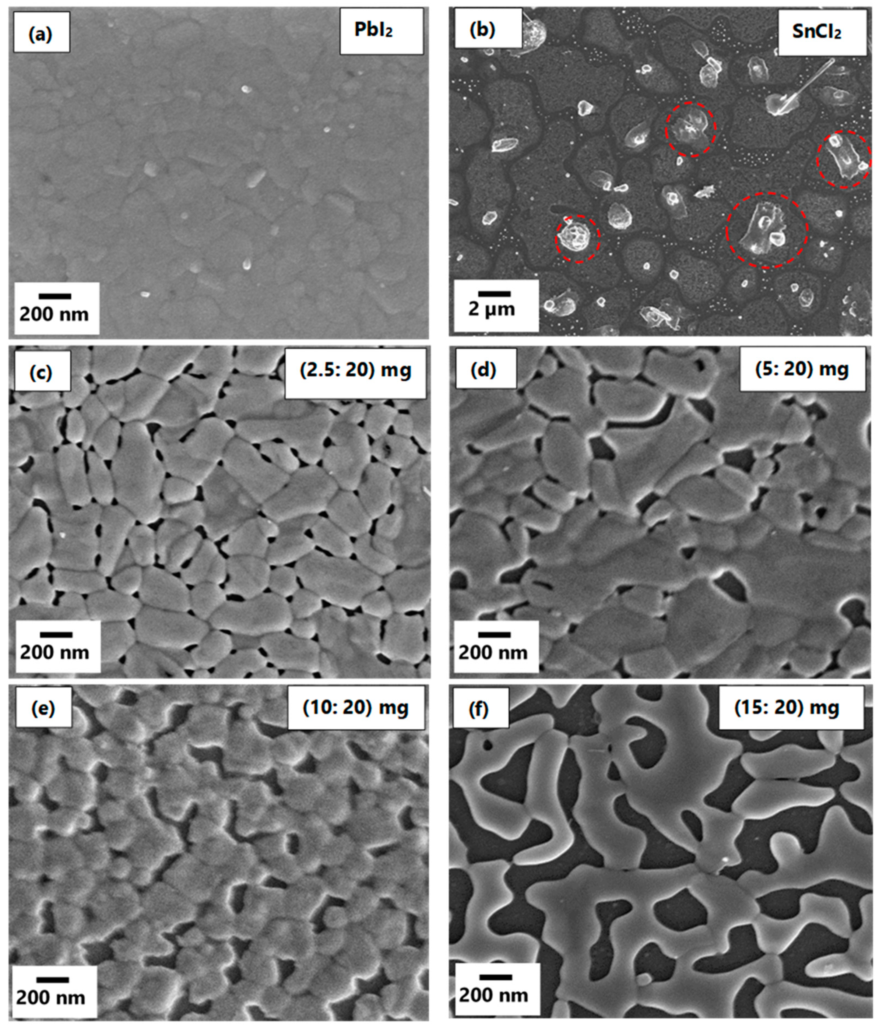
3.1.1. Surface Morphology

Throughout the discussion of the precursor films, samples will be referred to according to the SnCl2: PbI2 mass ratio used during the preparation of these precursor films. It is observed from the SEM micrographs in Figure 1a that PbI2 form a highly compact film composed of large grains that are tightly packed across the whole substrate. This behavior is consistent with that observed from the literature [66,67,68]. From Figure 1b, it is observed that SnCl2 forms randomly shaped, distinguishable islands with clearly defined boundaries. Furthermore, the SnCl2 forms clusters or agglomerates that are circled in red in Figure 1b. This SEM micrograph is different from those obtained by R. Felix et al. for SnCl2 films that were deposited using a 4-pocket evaporator attached to the ultra-high vacuum (UHV) deposition chamber [69]. Their results suggested that the growth mechanism of the SnCl2 film is divided into two-part; the lateral formation of the seeding layer followed by the vertical growth of the SnCl2 islands [69]. This suggests that our film might have reacted with moisture to form impurities such as tin oxide or hydrogen chloride since their films were prepared and studied in the system without exposure to ambient air conditions.
Figure 1c,d shows the SEM micrographs of mixed PbI2-SnCl2 compound films composed of different amount of SnCl2 (i.e., 2.5 mg, 5 mg, 10 mg, and 15 mg mixed with 20 mg of PbI2). Overall, it is observed that the presence of PbI2 improves the quality of the film of SnCl2. Figure 1c ((2.5:20) mg) depicts a film composed of clearly defined grains with grain sizes in the range between 200–400 nm and a high density of small-sized pores. Increasing the amount of SnCl2 to 5 mg in the film results in the coalescing of the small grains thereby forming larger grains. This sample still possesses low surface coverage due to the increase in the size of pores (Figure 1d). Figure 1e,f show that further increasing the amount of SnCl2 in the mixed metal-halide compound results in the deterioration of the quality of the films, hence, the observed disordered films with a larger number of pores that extend through the film to the substrate, which resulted in poor surface coverage. The thickness evolution of the compound films upon the increase of SnCl2 amount was measured using Dektak profilometer and plotted in Figure S2a in the supporting information (Supplementary Materials). It is observed from Figure S1a that the thickness of the films increases linearly as the amount of SnCl2 that was added in the crucible increases.

3.1.2. Rutherford Backscattering Spectrometry (RBS)

RBS was used for the determination of the stoichiometry and the depth profiles of the films. Figure 2a shows the experimental RBS spectra of PbI2 and mixed SnCl2-PbI2 compound thin films. Energy X-ray dispersive spectroscopy (EDS) data, not shown, was used for initial composition as required by SIMNRA software to begin the fitting process; with the simulated RBS spectra provided in Figure S2. The PbI2 film (black) shows two peaks of alpha particles backscattered from Pb and I atoms with surface energies of 2826.9 keV and 2694.2 keV, respectively. Although this is a single-layered film, the Pb peak appears at higher energy as compared to the I peak due to the difference in their atomic masses. This spectrum (i.e., PbI2 film) could be simulated using two layers with a total thickness and the average stoichiometry of 3.61 × 10¹⁷ atoms/cm2 and Pb0.35I0.65, respectively. Refer to Table 1 below for layer-by-layer details. The stoichiometry of the PbI2 film reported in this work corresponds to that reported by Popov et al. [70] and Tsevas et al. [71].
It can be observed from Figure 2a that mixing SnCl2 and PbI2 for the formation of compound films results; (i) in the quenching of the Pb peak intensity, (ii) peak broadening toward lower energies of iodine peak because of Sn peak with a surface energy of 2694.2 keV, which is close to the ions scattered from iodine, (iii) the development of Cl peak with a surface energy of 1952.9 keV. The addition of more SnCl2 in the mixed SnCl2-PbI2 compound films results in the progressive quenching of the Pb peak intensity and Sn/I peak broadening, as can be seen from Figure 2a. The quenching of scattering yield from the Pb atoms (especially at lower energies) as the amount of SnCl2 is increased implies that there is a spontaneous reaction between SnCl2 and PbI2 during the deposition, which might have been facilitated by the diffusion of surface atoms toward the substrate and/or the migration of bottom atoms toward the surface of the films. The Sn/I peak broadening and increasing intensity of Cl peaks indicate the progressive increase of Sn and Cl concentrations within the mixed SnCl2-PbI2 compound films.
Since the concentration of Sn increases upon the addition of SnCl2, the quenching of Sn/I peaks suggest that Cl atoms replace some I atoms in the mixed SnCl2-PbI2 compound films. These mixed SnCl2-PbI2 compound films that were deposited using different amount of SnCl2, i.e., 2.5 mg (red), 5 mg (blue), 10 mg (magenta), and 15 mg (green) mixed with 20 mg of PbI2 were simulated using three layers with a total thickness (×1017 atoms/cm2) and average stoichiometry of 4.22 & Pb0.24Sn0.11I0.30Cl0.36, 4.59 & Pb0.23Sn0.21I0.11Cl0.43, 4.94 & Pb0.23Sn0.27I0.04Cl0.45 and 6.01 & Pb0.19Sn0.30I0.02Cl0.48, respectively. Refer to Table 1 for the layer-by-layer details. It is noted from the table that surface layers of the films have more Pb atoms compared to the bottom layers that have more Sn atoms. This suggests that the SnCl2-PbI2 compound films formation is divided into two; (i) the deposition of the SnCl2 layer first followed by (ii) the deposition of the PbI2. The films were deposited on a glass substrate, which could be simulated with a thickness and stoichiometry of 3.50 × 10²² atoms/cm2 and Si0.19O0.72Al0.05Ba0.04As0.003, which correlates to what was obtained by Kumar et al. [72]. Figure 2b shows the compositional ratios of Sn/(Sn + Pb) and (Cl/Cl + I) deposited on the films. It can be observed from Figure 2b that the increased amount of SnCl2 in the source boat translated to the increase in Sn and Cl atoms in the films. A similar trend is portrayed by both Sn and Cl in comparison to Pb and iodine, respectively. This suggests that the separation distance between the source and the substrate is within the average migration distance of the vapors.

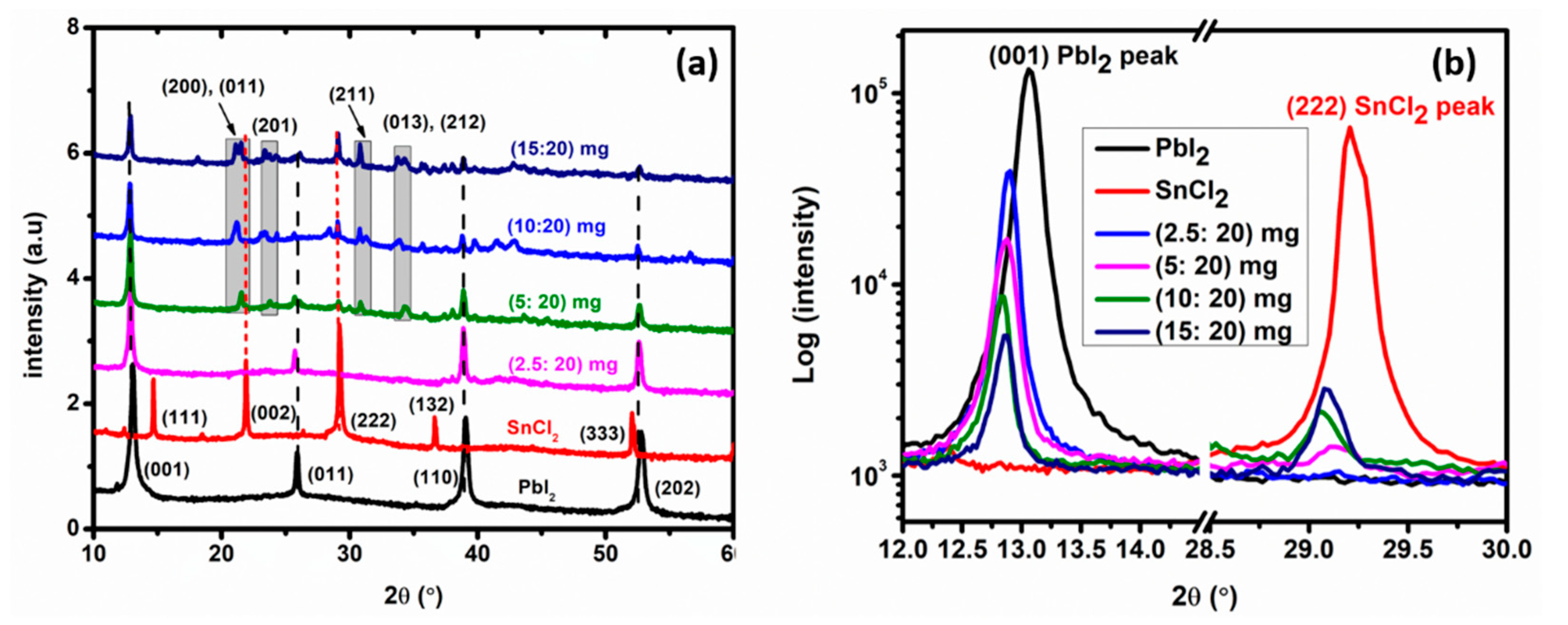
3.1.3. Crystal Structure and Phase Composition

X-ray diffraction (XRD) was employed to understand the effect of the SnCl2 content on the structure of the SnCl2-PbI2 compound thin films. Figure 3a shows XRD patterns of PbI2 thin film, SnCl2 thin film, and SnCl2-PbI2 compound films as named according to the amount of SnCl2 used. On one hand, the PbI2 thin-film depicted peaks located at 2θ values of 13.05°, 25.90°, 39.05°, and 52.77° assigned to (001), (011), (110), and (202) lattice planes, respectively. This PbI2 film formed a hexagonal structure, P321 space group (ICSD code: 01-075-0983), with the lattice parameters, a and c, of 4.606 Å and 6.774 Å, respectively. On the other hand, the SnCl2 thin-film depicted peaks located at 2θ values of 14.66°, 21.90°, 29.21°, 36.64°, 52.06°, and 60.14° ascribed to (111), (002), (222), (132), (333), and (062) lattice planes, respectively. It turns out that the film formed is not pure SnCl2, rather hydrated tin chloride (i.e., [SnCl4(H2O)2]3H2O) film with a monoclinic structure, C12/c1 space group (COD ID: 1534841), with the lattice parameters, a, b and c, of 7.760 Å, 9.555 Å, and 4.483 Å, respectively [73].
It is believed that as the SnCl2 film was deposited in the chamber, it reacted with and absorbed the ambient moisture upon exposure to the environment during the transfer of the sample. For mixed SnCl2-PbI2 films, it is observed from Figure 3a that the prominent Bragg diffraction peaks correspond to that of [SnCl4(H2O)2]3H2O and Pbl2 phases, indicating mixed-phase compounds. Also, low-intensity diffraction peaks unrelated to [SnCl4(H2O)2]3H2O) and/or PbI2 are observed for the 5, 10, and 15 mg SnCl2 samples. These peaks were located at 2θ values of 21.10°, 21.52°, 23.37°, 30.82°, 33.73°, and 34.28° which were ascribed to (200), (011), (201), (211), (013), and (212) lattice planes, respectively. These peaks, which are highlighted in grey in Figure 3a belonged to tin chloride iodide (SnClI) which form an orthorhombic structure, Pnma space group (ICSD code: 01-073-0826), with the lattice parameters, a, b, and c, of 8.42 Å, 4.43 Å and 10.04 Å, respectively. Figure 3b shows the (001) and (222) peaks of the SnCl2-PbI2 compound films, compared to that of PbI2 and SnCl2, respectively. It is observed in Figure 3b that the intensity of the (222) peak, which corresponds to [SnCl4(H2O)2]3H2O, increases as the amount of Sn increases in the film. The decrease in intensity of the (001) peak intensity, which corresponds to the PbI2, as the amount of Sn content increases supports the RBS discussion. Also, all the (001) peaks of SnCl2-PbI2 compound films shift toward lower 2θ angles with increasing SnCl2 concentration. This peak shift is due to the change in the chemical composition that could be ascribed to the chemical pressure caused by the change in lattice parameters [74,75]. The overall decrease in the peak intensities as the concentration of Sn increases suggests poor periodicity in the newly formed compound structures.

3.1.4. Optical Properties

The optical absorption spectra of PbI2, SnCl2, and the mixed SnCl2-PbI2 compound thin films was recorded as a function of wavelength in the range of (200–750) nm at room temperature, as shown in Figure 4a. The absorption onsets of the SnCl2 and PbI2 thin films were found to be at about 316 and 512 nm, respectively [66,76,77,78]. Furthermore, SnCl2 thin-film depicts an absorption peak centered at about 254 nm, while the PbI2 film depicts a characteristic absorption peak centered at about 405 nm, featuring a shoulder at 497 nm [66,77]. The absorption peak centered at about 252 nm is the contribution from the glass substrate on which the films were deposited. Generally, upon mixing PbI2 with SnCl2, an increase in the optical absorption intensity of the films in the wavelength range between 250–400 nm is observed, ascribed to the increase in the thickness of the films. The most noticeable feature in the optical properties of the mixed SnCl2-PbI2 compound thin films in comparison to that of pure PbI2 films is the red-shift of absorption onset. This necessitated the calculation of the optical band gap of the materials under investigation. The direct allowed band gap transition values were obtained by extrapolating the linear portion of the (αhv)2 versus hv plot, as depicted in Figure S3 in the support information. The corresponding values of Eg were found and plotted in Figure 4b. The Eg values increase from 2.42 eV for the PbI2 film to 3.31 eV for the mixed SnCl2-PbI2 compound film (15:20 mg) as the concentration of SnCl2 increases. The increase in the Eg confirms increasing concentrations of Sn in the films, since the Eg of SnCl2 is 3.92 eV. This further supports and confirms the RBS and XRD results.

3.2. Perovskite Structure-Property Relationships

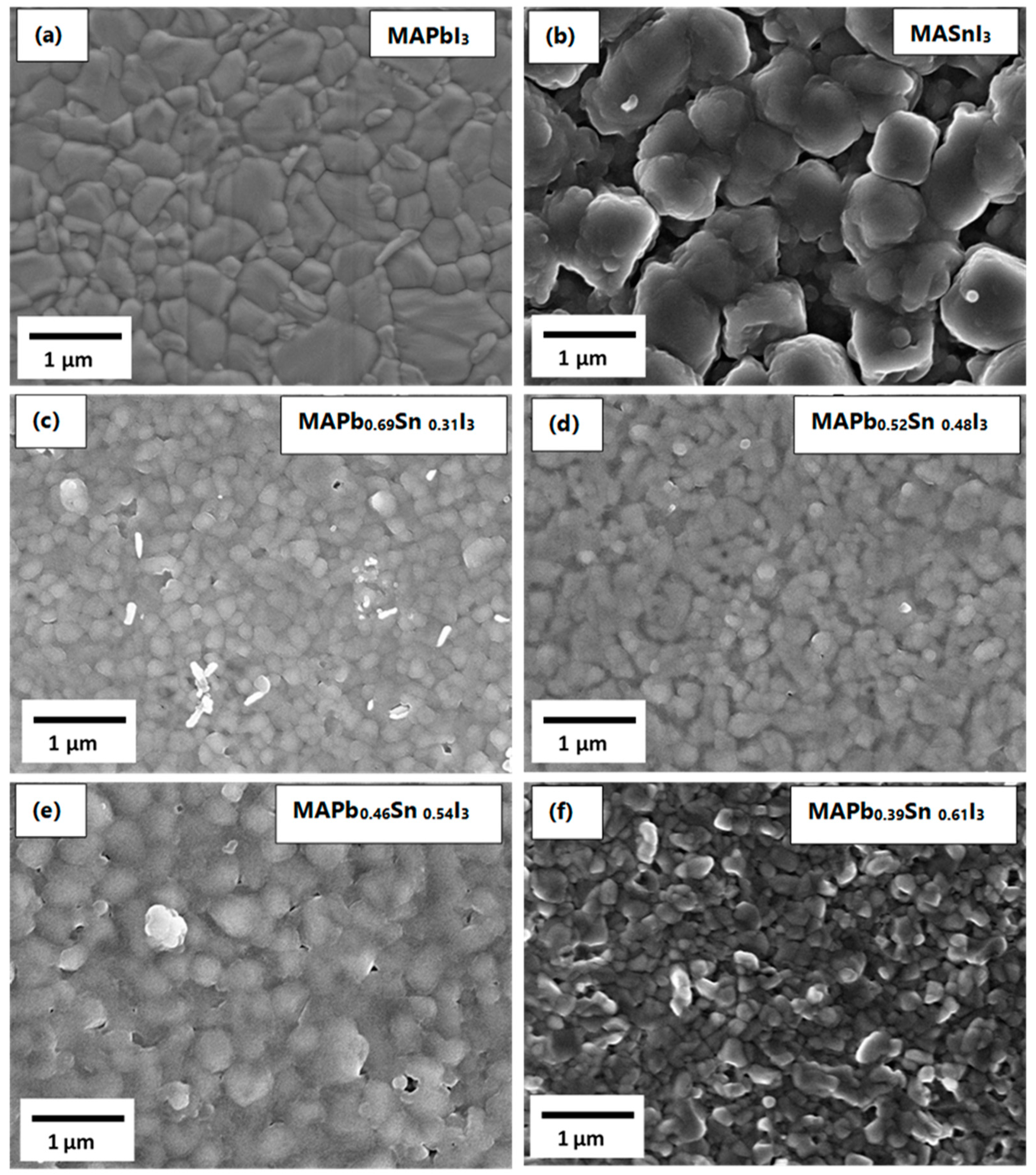
3.2.1. Surface Morphology

Figure 5 shows the top view SEM images of the Pb-based, Sn-based and Sn-Pb based perovskite films prepared using the precursor films that were discussed in the previous section. Compared with the precursor films in Figure 1, there are improvements in the grain size and surface coverage of the perovskite films. It is clear from the morphology in Figure 5a that MAPbI3 film is composed of well-defined, large grains (~1 µm) that are compact across the entire surface. The MASnI3 film is also composed of large grains, but with a porous morphology forming agglomerates, Figure 5b, which is due to the disorganized hydrated SnCl2 precursor film shown in Figure 1b. In the case of mixed metal-based perovskites, the crystal sizes of the films decrease as compared to the pure metal-based perovskite, Figure 5c,d. There is no significant difference in the surface morphology of the SnCl2-PbI2 compound films, except for an increased in roughness as the Sn concentration increases.
It is worth noting that the poly-porous morphology that was observed for mixed SnCl2-PbI2 compound films in Figure 1, improved to become compact perovskite films composed of crystals covering the entire surface. This is attributed to the MAI penetrating through the pores leading to sufficient reaction between mixed metal halides and MAI, thus forming completely converted perovskites. It is confirmed in Figure S1b that the thickness and the roughness of the films increase as the concentration of Sn increases. However, a massive increase in the perovskite films is attributed to the conversion process, i.e., the exposure of the precursor films to MAI vapor at a substrate temperature of 85 °C. The thickness increased by a factor of about 1.7 from the precursor films to the perovskite films, which indicates optimum conversion parameters.

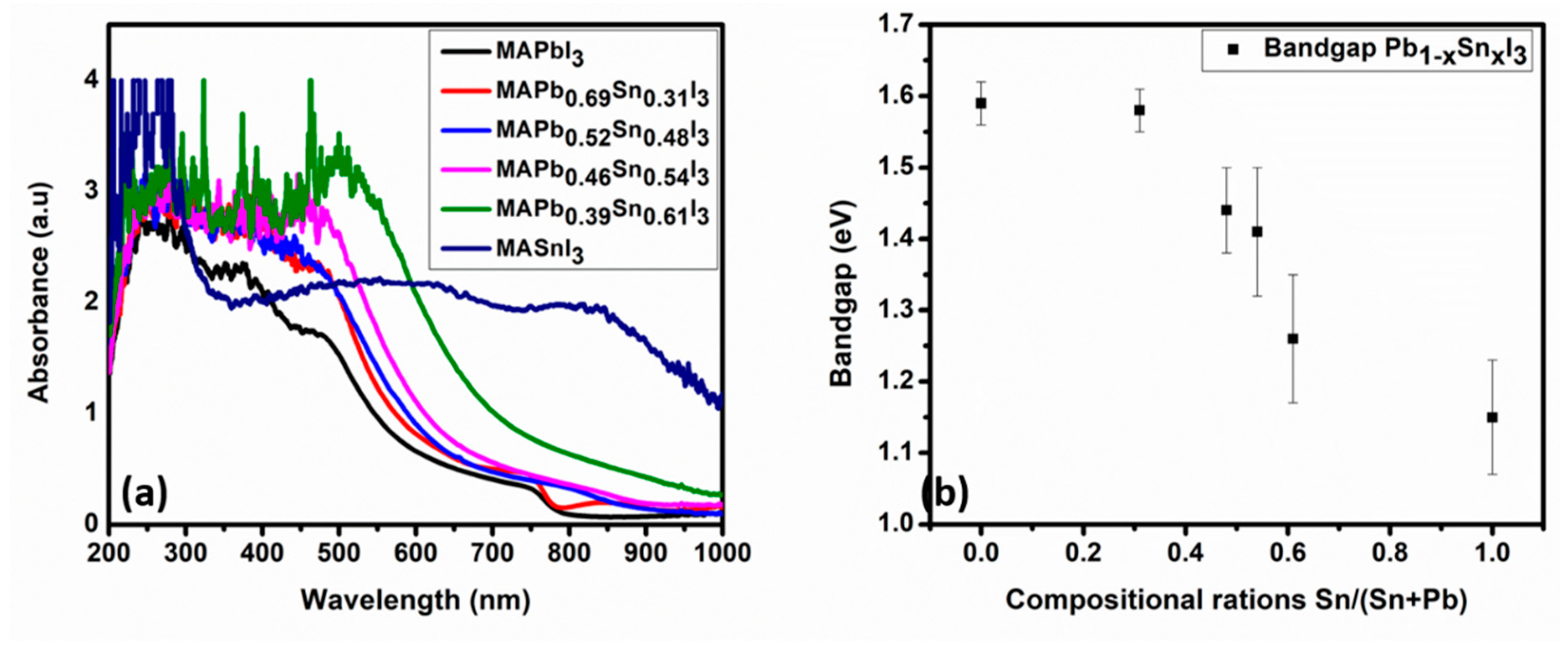
3.2.2. Crystal Structure and Optical Properties

The XRD patterns of the perovskite films obtained from PbI2, SnCl2 and mixed SnCl2: PbI2 compound films are shown in Figure 6a. All the perovskite films possess similar patterns in terms of peak positions with the exception of the diffraction intensities. This suggests that iodine from the MAI replaces the Cl in SnCl2 and mixed SnCl2-PbI2 compound films [79]. Also, the PbI2 stabilizes the mixed metal halide compound films and reduces their susceptibility to moisture compared to the SnCl2 film. The peaks located at 2θ values of 14.20°, 24.57°, 28.49°, 31.96°, 40.98°, 43.30°, and 50.29° could be ascribed to (110), (202), (220), (222), (400), (420), and (404) lattice planes, respectively. According to the crystallography open-sources database (COD), these perovskite films form a tetragonal structure with I4cm space group (COD ID: 4335638, 4335641, 4335636, for the Pb-based, mixed Sn-Pb based, and Sn-based perovskites, respectively) [80]. The MAPbI3 and MAPb0.69Sn0.31I3 show additional peaks at 12.66° (denoted by an asterisk) and 58.97° ascribed to PbI2 (001) and MAPbI3 (440) lattice plane, respectively. The PbI2 peak denotes slightly incomplete conversions. This could have been because of tightly packed crystals in the PbI2 and Pb0.24Sn0.11I0.30Cl0.36 compound films, which could limit the infusion of MAI during the conversion stage.
The highly intense MAPbI3 sample peaks are ascribed to the neat, large, and uniformly distributed crystals, while the MASnI3 sample with second-most intense peaks is ascribed only to its large crystals. The lower peak intensities of MAPb1−x SnxI3 films denoted poor crystallinity of these perovskite films compared to the MAPbI3 film. Figure 6b shows the inverse relation of the unit cell volume with increasing concentration of Sn. The unit cell volume of the MAPbI3 perovskite decreases from 988.4 Å3 to about 983.3 Å3 upon the incorporation of Sn in the structure, which is coherent as the volume of the MASnI3 perovskite is 970.3 Å3. This is due to the smaller ionic radius of Sn compared to that of Pb. Table 2 shows the lattice constants, FWHM of (110) diffraction peak located at 2θ value of 14.2° and the average crystallite size (D) estimated using Scherrer equation, D = kλ/ꞵcosθ, where k = 0.89, λ = 0.154 nm, and θ = 14.3° are Scherrer’s constant, X-ray wavelength, and Bragg diffraction angle, respectively. The average crystallite size of the pure perovskites, i.e., MAPbI3 and MASnI3 are 71.9 nm and 65.6 nm, respectively. These values are larger than those obtained for mixed metal perovskites as evident from Table 2. This agrees with the SEM results; considering that the pure perovskites films possessed larger grains compared to those of mixed metal perovskites. The crystallite sizes decreased upon the increasing concentration of Sn in the perovskite films from 71.9 nm for MAPbI3 to 50.9 nm for MAPb0.39Sn0.61I3. The crystallite size of MAPb0.69Sn0.31I3 was calculated to be 45.8 nm, which is considered as an outlier as observed in Figure S4a.
The UV-Vis absorption spectra of the perovskite films are shown in Figure 7a. The MAPbI3 depicts characteristic absorption peaks centered at the wavelength of about 357 nm and 470 nm and a shoulder at 747 nm, whereas the MASnI3 perovskite shows absorption extending from 365 to 1000 nm with characteristic absorption peaks centered at about 536 and 850 nm. The absorption peak centered at about 252 nm is the contribution from the glass substrate on which the films were deposited. The increase in the optical absorption intensity upon the addition of Sn in the structure is attributed to the increase in the perovskite films thicknesses. It is noticed from Figure 7a that the absorption band edges of the films are not sharp and well-defined. This produces band tails that extend into the band gap, which increases with increasing Sn concentration that is associated with an increasing defect-concentration in the films. These band tails, also referred to as the Urbach tails, is associated with the Urbach energy (Eu) that can be extracted using the relation α = α0exp(E/Eu), where α is the absorption coefficient and E the photon energy.
Figure 7b shows the band gap (Eg) evolution obtained from Tauc plots depicted in Figure S5 in the supplementary material. The incorporation of Sn decreases the band gap of the films from about 1.59 eV for MAPbI3 to about 1.26 eV for MAPb0.39Sn0.61I3 and the lowest Eg of 1.15 eV was obtained for MASnI3, as depicted in Figure 7b and Table 3. Apart from absorption band-edge shift toward high wavelength, Sn incorporation also retards the structure of MAPbI3 slightly, augmented by the diminishing of MAPbI3 characteristic absorption features, which corresponds to the results in the literature [31,32,33,67]. However, contrary to recent studies, our results do not show absorption bandgap bowing behavior, which is the reduction of the Eg of the mixed metal perovskites to values below the end compounds i.e., MAPbI3 (1.59 eV) and MASnI3 (1.15 eV) in this case. There is an ongoing debate about the origin and magnitude of the bandgap bowing in mixed metal perovskites; whether it is due to the chemical effects, structural effects, or a combination of both [81,82,83]. Nonetheless, it is believed that the 61% maximum Sn concentration employed in this study is below the bandgap bowing threshold for the deposition system and the parameters used.
The Eu values, which equates to the widths of the band tails of the defect states in the band gap and thus the density of disorder in the films, are tabulated in Table 3 and were obtained by plotting the natural logarithm of the absorption coefficient ln (α) as a function of photon energy and then taking the reciprocal of the slope from the linear part of the curve [84,85], as shown in Figure S6. The MAPbI3 has an Eu of about 70 meV, which remains constant for the MAPb0.69Sn0.31I3 film with the lowest concentration of Sn. Further increasing the concentration of Sn increased the Eu to about 280 meV for MAPb0.39Sn0.61I3, and the MASnI3 showed the highest Eu of about 530 eV. The increasing trend of Eu with increasing concentration of Sn was observed by Zhao et al. and Li et al. [13,86]. This is ascribed to the increased oxygen defect centers in the thin films affiliated with the increased oxidation of Sn2+ to Sn4+ [13,86]. This observation of an increasing Eu with increasing Sn concentration confirms the XRD suggestion that the incorporation of excessive amount of Sn in the Pb based perovskites results in poor crystallization and the high-level defect density that is induced by Sn oxidation.

4. Conclusions

We synthesized mixed metal halide perovskite thin films by two step-sequential CVD, which included the deposition of mixed SnCl2-PbI2 compound as the precursor films and subsequently exposing them to MAI for conversion into perovskites. A controlled the concentration of Sn in the perovskite films was demonstrated, as quantified by RBS. The micrographs of these precursor films depicted a poly-porous surface with pores extending deep to the substrate with an increasing concentration of Sn in the film. These pores might have been helpful in the conversion processes in terms of acting as the passage through which MAI infiltrated the films thus leading to complete conversions into perovskites rather than partial conversions. All the perovskite films depicted similar XRD patterns corresponding to a tetragonal structure with I4cm space group regardless of the precursor films having different crystal structures which is positive since the aim of the study was to partially replace Pb atoms with Sn without destroying the core of MAPbI3 perovskite structure. This resulted in the decrease of the unit volume of the perovskites from about 988.4 Å3 for MAPbI3 to about 983.3 Å3 for MAPb0.39Sn0.61I3 which was attributed to the smaller atomic radius of Sn than that of Pb. Therefore, the inclusion of Sn in the structure did indeed influence the properties of the resulted perovskite films manifested by the decrease in band gap from about 1.59 eV for MAPbI3 to 1.26 eV for MAPb0.39Sn0.61I3 and an increased defect density in the band gap that is associated with the increased oxidation of Sn2+ to Sn4+.

Supplementary Materials

The following are available online at https://www.mdpi.com/article/10.3390/ma14133526/s1, Figure S1: Thickness evolution upon different Sn compositional ratios of (a) precursor films and (b) perovskite films. It is observed from the Figure that the thickness of the film increases as the amount of Sn content increases, Figure S2: Experimental and simulated RBS spectra of (a) PbI2 thin film, and (b–e) mixed SnCl2-PbI2 compound thin films i.e., (2.5:20) mg, (5:20) mg, (10:20) mg and (15:20) mg, respectively. The simulated spectra in Figure S2a,b were obtained using two layers with a total thickness and the average stoichiometry of 3.61 × 10¹⁷ atoms/cm2 and Pb0.35I0.65 and 4.22 & Pb0.24Sn0.11I0.30Cl0.36, respectively. While the spectra in Figure S2c–e were simulated using three layers with a total thickness (×1017 atoms/cm2) and average stoichiometry of, 4.59 & Pb0.23Sn0.21I0.11Cl0.43, 4.94 & Pb0.23Sn0.27I0.04Cl0.45 and 6.01 & Pb0.19Sn0.30I0.02Cl0.48, respectively, Figure S3: Tauc Plots for the bandgap measurement from the UV-Vis spectra of (a) PbI2 film, (b) SnCl2 film and (c–f) mixed SnCl2-PbI2 compound films. The bang gaps of PbI2 and SnCl2 films were found to be 2.42 eV and 3.92 eV, respectively. While the band gaps of mixed SnCl2-PbI2 compound films i.e., (2.5:20) mg, (5:20) mg, (10:20) mg and (15:20) mg were found to be 2.79 eV, 2.93 eV, 3.10 eV and 3.31 eV, respectively, Figure S4: Crystallite size evolution upon increasing the concentration of Sn, (a) includes MAPbI3 and all the mixed metal perovskite. (b) Excludes the 45.8 nm average crystallite size for MAPb0.69Sn0.31I3 perovskite and includes the trendline to guide the eye, Figure S5: Tauc Plots for the bandgap measurement from the UV-Vis spectra of (a) MAPbI3 film, (b–e) mixed metal perovskite films and (f) MASnI3 film. The bang gaps of MAPbI3 and MASnI3 films were found to be 1.59 eV and 1.15 eV, respectively. While the band gaps of mixed metal perovskite films i.e., MAPb0.69Sn0.31I3, MAPb0.52Sn0.48I3, MAPb0.46Sn0.54I3 and MAPb0.39Sn0.61I3 were found to be 1.58 eV, 1.44 eV, 1.41 eV and 1.26 eV, respectively, Figure S6: Urbach energy approximation plots of (a) MAPbI3 film, (b–e) mixed metals perovskite films and (f) MASnI3 film. The Urbach energies of MAPbI3 and MASnI3 films were found to be 0.07 eV and 0.53 eV, respectively. While the Urbach energies of mixed metal perovskite films i.e., MAPb0.69Sn0.31I3, MAPb0.52Sn0.48I3, MAPb0.46Sn0.54I3 and MAPb0.39Sn0.61I3 were found to be 0.06 eV, 0.22 eV, 0.26 eV and 0.28 eV, respectively.

Author Contributions

Conceptualization, C.J.A. and S.S.M.; methodology, S.S.M., S.N.; software, C.J.A.; validation, C.J.A., S.N. and A.S.B.; formal analysis, S.S.M.; investigation, S.S.M.; resources, C.J.A.; data curation, F.C. and C.M.; writing—original draft preparation, S.S.M.; writing—review and editing, S.S.M.; visualization, S.S.M., C.J.A. and S.N.; supervision, C.J.A. and A.S.B.; project administration, C.J.A.; funding acquisition, C.J.A. All authors have read and agreed to the published version of the manuscript.

Funding

The authors would like to acknowledge the South African National Research Foundation (NFR) (Grant No: 117874, 103621, 92520 and 93212) and Armaments Corporation of South Africa (ARMSCOR), DESUP project, for financial support.

Institutional Review Board Statement

Not applicable.

Informed Consent Statement

Not applicable.

Data Availability Statement

The data that support the findings of this study are available from the corresponding author, upon reasonable request.

Conflicts of Interest

The authors declare no conflict of interest.

References

  1. Wenk, H.; Bulakh, A. Minerals: Their constitution and origin. Can. Min. J. 2004, 125, 7. [Google Scholar]
  2. Kojima, A.; Teshima, K.; Shirai, Y.; Miyasaka, T. Organometal halide perovskites as visible-light sensitizers for photovoltaic cells. J. Am. Chem. Soc. 2009, 131, 6050–6051. [Google Scholar] [CrossRef] [PubMed]
  3. Podolsky, B.; Rosen, N.; Clauser, J.F.; Steinberg, A.M.; Chiao, R.Y.; Vaziri, A.; Weihs, G.; Zeilinger, A.; Bennink, R.S.; Bentley, S.J.; et al. Efficient Hybrid Solar Cells Based on Meso-Superstructured Organometal Halide Perovskites. Science 2012, 338, 643–648. [Google Scholar]
  4. Burschka, J.; Pellet, N.; Moon, S.J.; Humphry-Baker, R.; Gao, P.; Nazeeruddin, M.K.; Grätzel, M. Sequential deposition as a route to high-performance perovskite-sensitized solar cells. Nature 2013, 499, 316–319. [Google Scholar] [CrossRef]
  5. Liu, M.; Johnston, M.B.; Snaith, H.J. Efficient planar heterojunction perovskite solar cells by vapour deposition. Nature 2013, 501, 395–398. [Google Scholar] [CrossRef]
  6. Jeon, N.J.; Noh, J.H.; Kim, Y.C.; Yang, W.S.; Ryu, S.; Seok, S. Il Solvent engineering for high-performance inorganic-organic hybrid perovskite solar cells. Nat. Mater. 2014, 13, 897–903. [Google Scholar] [CrossRef]
  7. Green, M.A.; Ho-Baillie, A.; Snaith, H.J. The emergence of perovskite solar cells. Nat. Photonics 2014, 8, 506–514. [Google Scholar] [CrossRef]
  8. Yang, W.S.; Park, B.W.; Jung, E.H.; Jeon, N.J.; Kim, Y.C.; Lee, D.U.; Shin, S.S.; Seo, J.; Kim, E.K.; Noh, J.H.; et al. Iodide management in formamidinium-lead-halide-based perovskite layers for efficient solar cells. Science 2017, 356, 1376–1379. [Google Scholar] [CrossRef] [Green Version]
  9. Chan, S.H.; Chang, Y.H.; Wu, M.C. High-performance perovskite solar cells based on low-temperature processed electron extraction layer. Front. Mater. 2019, 6, 1–7. [Google Scholar] [CrossRef] [Green Version]
  10. Frolova, L.A.; Davlethanov, A.I.; Dremova, N.N.; Zhidkov, I.; Akbulatov, A.F.; Kurmaev, E.Z.; Aldoshin, S.M.; Stevenson, K.J.; Troshin, P.A. Efficient and stable MAPbI3-based perovskite solar cells using polyvinylcarbazole passivation. J. Phys. Chem. Lett. 2020, 11, 6772–6778. [Google Scholar] [CrossRef] [PubMed]
  11. Shockley, W.; Queisser, H.J. Detailed balance limit of efficiency of p-n junction solar cells. J. Appl. Phys. 1961, 32, 510–519. [Google Scholar] [CrossRef]
  12. Im, J.; Stoumpos, C.C.; Jin, H.; Freeman, A.J.; Kanatzidis, M.G. Antagonism between spin-orbit coupling and steric effects causes anomalous band gap evolution in the perovskite photovoltaic materials CH3NH3Sn1−xPbxI3. J. Phys. Chem. Lett. 2015, 6, 3503–3509. [Google Scholar] [CrossRef]
  13. Zhao, B.; Abdi-Jalebi, M.; Tabachnyk, M.; Glass, H.; Kamboj, V.S.; Nie, W.; Pearson, A.J.; Puttisong, Y.; Gödel, K.C.; Beere, H.E.; et al. High open-circuit voltages in tin-rich low-bandgap perovskite-based planar heterojunction photovoltaics. Adv. Mater. 2017, 29. [Google Scholar] [CrossRef]
  14. Kazim, S.; Nazeeruddin, M.K.; Grätzel, M.; Ahmad, S. Perovskite as light harvester: A game changer in photovoltaics. Angew. Chem. Int. Ed. 2014, 53, 2812–2824. [Google Scholar] [CrossRef]
  15. Paquin, F.; Rivnay, J.; Salleo, A.; Stingelin, N.; Silva, C. Multi-phase semicrystalline microstructures drive exciton dissociation in neat plastic semiconductors. J. Mater. Chem. C 2015, 3, 10715–10722. [Google Scholar] [CrossRef] [Green Version]
  16. Serrano-lujan, L.; Espinosa, N.; Larsen-olsen, T.T.; Abad, J.; Urbina, A.; Krebs, F.C. Tin- and lead-based perovskite solar cells under scrutiny: An environmental perspective. Adv. Energy Mater. 2015, 15, 1–5. [Google Scholar] [CrossRef]
  17. Stranks, S.D.; Nayak, P.K.; Zhang, W.; Stergiopoulos, T.; Snaith, H.J. Formation of thin films of organic-inorganic perovskites for high-efficiency solar cells. Angew. Chem. Int. Ed. 2015, 54, 3240–3248. [Google Scholar] [CrossRef] [PubMed] [Green Version]
  18. Chen, Y.; He, M.; Peng, J.; Sun, Y.; Liang, Z. Structure and growth control of organic–inorganic halide perovskites for optoelectronics: From polycrystalline films to single crystals. Adv. Sci. 2016, 3. [Google Scholar] [CrossRef] [PubMed] [Green Version]
  19. Hoefler, S.F.; Trimmel, G.; Rath, T. Progress on lead-free metal halide perovskites for photovoltaic applications: A review. Mon. Chem. 2017, 148, 795–826. [Google Scholar] [CrossRef] [Green Version]
  20. Stroyuk, O. Lead-free hybrid perovskites for photovoltaics. Beilstein J. Nanotechnol. 2018, 9, 2209–2235. [Google Scholar] [CrossRef]
  21. Liu, C.; Li, W.; Fan, J.; Mai, Y. A brief review on the lead element substitution in perovskite solar cells. J. Energy Chem. 2018, 27, 1054–1066. [Google Scholar] [CrossRef]
  22. Zhou, D.; Zhou, T.; Tian, Y.; Zhu, X.; Tu, Y. Perovskite-based solar cells: Materials, methods, and future perspectives. J. Nanomater. 2018, 2018. [Google Scholar] [CrossRef]
  23. Zhang, Q.; Hao, F.; Li, J.; Zhou, Y.; Wei, Y.; Lin, H. Perovskite solar cells: Must lead be replaced–and can it be done? Sci. Technol. Adv. Mater. 2018, 19, 425–442. [Google Scholar] [CrossRef] [Green Version]
  24. Ansari, M.I.H.; Qurashi, A.; Nazeeruddin, M.K. Frontiers, opportunities, and challenges in perovskite solar cells: A critical review. J. Photochem. Photobiol. C Photochem. Rev. 2018, 35, 1–24. [Google Scholar] [CrossRef]
  25. Jena, A.K.; Kulkarni, A.; Miyasaka, T. Halide perovskite photovoltaics: Background, status, and future prospects. Chem. Rev. 2019, 119, 3036–3103. [Google Scholar] [CrossRef]
  26. Ke, W.; Kanatzidis, M.G. Prospects for low-toxicity lead-free perovskite solar cells. Nat. Commun. 2019, 1–4. [Google Scholar] [CrossRef]
  27. Ji, D.; Wang, S.; Zhang, H.; Wang, H.; Zhang, B.; Zhang, C.; Li, X. Why cannot all divalent cations completely substitute the Pb cations of CH3NH3PbI3 perovskite? Phys. Lett. 2019, 383, 2130–2138. [Google Scholar] [CrossRef]
  28. Wang, K.; Subhani, W.S.; Wang, Y.; Zuo, X.; Wang, H.; Duan, L.; Liu, S. Metal cations in efficient perovskite solar cells: Progress and perspective. Adv. Mater. 2019, 31, 1–17. [Google Scholar] [CrossRef]
  29. Liu, C.; Li, W.; Li, H.; Zhang, C.; Fan, J.; Mai, Y. C60 additive-assisted crystallization in CH3NH3Pb0.75Sn0.25I3 perovskite solar cells with high stability and efficiency. Nanoscale 2017, 9, 13967–13975. [Google Scholar] [CrossRef] [PubMed]
  30. Leijtens, T.; Prasanna, R.; Gold-Parker, A.; Toney, M.F.; McGehee, M.D. Mechanism of tin oxidation and stabilization by lead substitution in tin halide perovskites. ACS Energy Lett. 2017, 2, 2159–2165. [Google Scholar] [CrossRef]
  31. Gu, S.; Lin, R.; Han, Q.; Gao, Y.; Tan, H.; Zhu, J. Tin and mixed lead–tin halide perovskite solar cells: Progress and their application in tandem solar cells. Adv. Mater. 2020, 32, 1–16. [Google Scholar] [CrossRef]
  32. Ogomi, Y.; Morita, A.; Tsukamoto, S.; Saitho, T.; Fujikawa, N.; Shen, Q.; Toyoda, T.; Yoshino, K.; Pandey, S.S.; Ma, T.; et al. CH3NH3SnxPb(1−x)I3 perovskite solar cells covering up to 1060 nm. J. Phys. Chem. Lett. 2014, 5, 1004–1011. [Google Scholar] [CrossRef] [PubMed]
  33. Hao, F.; Stoumpos, C.C.; Chang, R.P.H.; Kanatzidis, M.G. Anomalous band gap behavior in mixed Sn and Pb perovskites enables broadening of absorption spectrum in solar cells. J. Am. Chem. Soc. 2014, 136, 8094–8099. [Google Scholar] [CrossRef] [PubMed]
  34. Yang, Z.; Rajagopal, A.; Chueh, C.; Jo, S.B.; Liu, B.; Zhao, T.; Jen, A.K. Stable low-bandgap Pb-Sn binary perovskites for tandem solar cells. Adv. Mater. 2016, 28, 8990–8997. [Google Scholar] [CrossRef]
  35. Calvo, M.E.; Hagfeldt, A. Optical analysis of CH3NH3SnxPb1-xI3 absorbers: A roadmap for perovskite-on-perovskite tandem solar cells. J. Mater. Chem. A 2016. [Google Scholar] [CrossRef] [Green Version]
  36. Eperon, G.E.; Leijtens, T.; Bush, K.A.; Prasanna, R.; Green, T.; Wang, J.T.W.; McMeekin, D.P.; Volonakis, G.; Milot, R.L.; May, R.; et al. Perovskite-perovskite tandem photovoltaics with optimized band gaps. Science 2016, 354, 861–865. [Google Scholar] [CrossRef] [Green Version]
  37. Liu, X.; Yang, Z.; Chueh, C.C.; Rajagopal, A.; Williams, S.T.; Sun, Y.; Jen, A.K.Y. Improved efficiency and stability of Pb-Sn binary perovskite solar cells by Cs substitution. J. Mater. Chem. A 2016, 4, 17939–17945. [Google Scholar] [CrossRef]
  38. Zhu, L.; Yuh, B.; Schoen, S.; Li, X.; Aldighaithir, M.; Richardson, B.J.; Alamer, A.; Yu, Q. Solvent-molecule-mediated manipulation of crystalline grains for efficient planar binary lead and tin triiodide perovskite solar cells. Nanoscale 2016, 8, 7621–7630. [Google Scholar] [CrossRef] [PubMed]
  39. Rajagopal, A.; Yang, Z.; Jo, S.B.; Braly, I.L.; Liang, P.W.; Hillhouse, H.W.; Jen, A.K.Y. Highly Efficient perovskite–perovskite tandem solar cells reaching 80% of the theoretical limit in photovoltage. Adv. Mater. 2017, 29, 1–10. [Google Scholar] [CrossRef] [PubMed]
  40. Tang, Z.K.; Xu, Z.F.; Zhang, D.Y.; Hu, S.X.; Lau, W.M.; Liu, L.M. Enhanced optical absorption via cation doping hybrid lead iodine perovskites. Sci. Rep. 2017, 7, 1–7. [Google Scholar] [CrossRef] [PubMed] [Green Version]
  41. Zhu, H.L.; Xiao, J.; Mao, J.; Zhang, H.; Zhao, Y.; Choy, W.C.H. Controllable crystallization of CH3NH3Sn0.25Pb0.75I3 perovskites for hysteresis-free solar cells with efficiency reaching 15.2%. Adv. Funct. Mater. 2017, 27. [Google Scholar] [CrossRef]
  42. Zong, Y.; Wang, N.; Zhang, L.; Ju, M.G.; Zeng, X.C.; Sun, X.W.; Zhou, Y.; Padture, N.P. Homogenous alloys of formamidinium lead triiodide and cesium tin triiodide for efficient ideal-bandgap perovskite solar cells. Angew. Chem. Int. Ed. 2017, 56, 12658–12662. [Google Scholar] [CrossRef]
  43. Li, L.; Zhang, F.; Hao, Y.; Sun, Q.; Li, Z.; Wang, H.; Cui, Y.; Zhu, F. High efficiency planar Sn-Pb binary perovskite solar cells: Controlled growth of large grains via a one-step solution fabrication process. J. Mater. Chem. C 2017, 5, 2360–2367. [Google Scholar] [CrossRef]
  44. Li, Y.; Sun, W.; Yan, W.; Ye, S.; Rao, H.; Peng, H.; Zhao, Z. 50% Sn-based planar perovskite solar cell with power conversion efficiency up to 13.6%. Adv. Energy Mater. 2016, 6, 1–7. [Google Scholar] [CrossRef]
  45. Lyu, M.; Zhang, M.; Cooling, N.A.; Jiao, Y.; Wang, Q.; Yun, J.H.; Vaughan, B.; Triani, G.; Evans, P.; Zhou, X.; et al. Highly compact and uniform CH3NH3Sn0.5Pb0.5I3 films for efficient panchromatic planar perovskite solar cells. Sci. Bull. 2016, 61, 1558–1562. [Google Scholar] [CrossRef] [Green Version]
  46. Zuo, F.; Williams, S.T.; Liang, P.; Chueh, C.; Liao, C.; Jen, A.K. Binary-metal perovskites toward high-performance planar-heterojunction hybrid solar cells. Adv. Mater. 2014, 26, 6454–6460. [Google Scholar] [CrossRef]
  47. Lin, G.; Lin, Y.; Huang, H.; Cui, R.; Guo, X.; Liu, B.; Dong, J.; Guo, X.; Sun, B. Novel exciton dissociation behavior in tin-lead organohalide perovskites. Nano Energy 2016, 27, 638–646. [Google Scholar] [CrossRef]
  48. Zhao, D.; Yu, Y.; Wang, C.; Liao, W.; Shrestha, N.; Grice, C.R.; Cimaroli, A.J.; Guan, L.; Ellingson, R.J.; Zhu, K.; et al. Low-bandgap mixed tin–lead iodide perovskite absorbers with long carrier lifetimes for all-perovskite tandem solar cells. Nat. Energy 2017, 2, 17018. [Google Scholar] [CrossRef]
  49. Tsai, C.M.; Wu, H.P.; Chang, S.T.; Huang, C.F.; Wang, C.H.; Narra, S.; Yang, Y.W.; Wang, C.L.; Hung, C.H.; Diau, E.W.G. Role of tin chloride in tin-rich mixed-halide perovskites applied as mesoscopic solar cells with a carbon counter electrode. ACS Energy Lett. 2016, 1, 1086–1093. [Google Scholar] [CrossRef]
  50. Liu, C.; Fan, J.; Li, H.; Zhang, C.; Mai, Y. Highly efficient perovskite solar cells with substantial reduction of lead content. Sci. Rep. 2016, 6, 1–8. [Google Scholar] [CrossRef] [PubMed] [Green Version]
  51. Kapil, G.; Ripolles, T.S.; Hamada, K.; Ogomi, Y.; Bessho, T.; Kinoshita, T.; Chantana, J.; Yoshino, K.; Shen, Q.; Toyoda, T.; et al. Highly efficient 17.6% tin-lead mixed perovskite solar cells realized through spike structure. Nano Lett. 2018, 18, 3600–3607. [Google Scholar] [CrossRef]
  52. Jiang, T.; Chen, Z.; Chen, X.; Chen, X.; Xu, X.; Liu, T.; Bai, L.; Yang, D.; Di, D.; Sha, W.E.I.; et al. Power conversion efficiency enhancement of low-bandgap mixed Pb-Sn perovskite solar cells by improved interfacial charge transfer. ACS Energy Lett. 2019, 4, 1784–1790. [Google Scholar] [CrossRef]
  53. Li, C.; Song, Z.; Zhao, D.; Xiao, C.; Subedi, B.; Shrestha, N.; Junda, M.M.; Wang, C.; Jiang, C.S.; Al-Jassim, M.; et al. Reducing saturation-current density to realize high-efficiency low-bandgap mixed tin–lead halide perovskite solar cells. Adv. Energy Mater. 2019, 9, 1–9. [Google Scholar] [CrossRef]
  54. Xu, X.; Chueh, C.C.; Yang, Z.; Rajagopal, A.; Xu, J.; Jo, S.B.; Jen, A.K.Y. Ascorbic acid as an effective antioxidant additive to enhance the efficiency and stability of Pb/Sn-based binary perovskite solar cells. Nano Energy 2017, 34, 392–398. [Google Scholar] [CrossRef] [Green Version]
  55. Yun, Y.; Cho, J.Y.; Heo, J.; Lee, S. Fabrication of MASnI3 and MASnxPb(1−x)I3 thin films by conversion from SnS thin film. Appl. Sci. Converg. Technol. 2018, 27, 169–172. [Google Scholar] [CrossRef] [Green Version]
  56. Ke, W.; Spanopoulos, I.; Tu, Q.; Hadar, I.; Li, X.; Shekhawat, G.S.; Dravid, V.P.; Kanatzidis, M.G. Ethylenediammonium-based “hollow” Pb/Sn perovskites with ideal band gap yield solar cells with higher efficiency and stability. J. Am. Chem. Soc. 2019, 141, 8627–8637. [Google Scholar] [CrossRef]
  57. Du, X.; Qiu, R.; Zou, T.; Chen, X.; Chen, H.; Zhou, H. Enhanced uniformity and stability of Pb–Sn perovskite solar cells via Me4NBr passivation. Adv. Mater. Interfaces 2019, 6, 1–7. [Google Scholar] [CrossRef]
  58. Tong, J.; Song, Z.; Kim, D.H.; Chen, X.; Chen, C.; Palmstrom, A.F.; Ndione, P.F.; Reese, M.O.; Dunfield, S.P.; Reid, O.G.; et al. Carrier lifetimes of >1 ms in Sn-Pb perovskites enable efficient all-perovskite tandem solar cells. Science 2019, 364, 475–479. [Google Scholar] [CrossRef]
  59. Lian, X.; Chen, J.; Zhang, Y.; Qin, M.; Li, J.; Tian, S.; Yang, W.; Lu, X.; Wu, G.; Chen, H. Highly efficient Sn/Pb binary perovskite solar cell via precursor engineering: A two-step fabrication process. Adv. Funct. Mater. 2019, 29, 1–9. [Google Scholar] [CrossRef]
  60. Klug, M.T.; Milot, R.L.; Milot, R.L.; Patel, J.B.; Green, T.; Sansom, H.C.; Farrar, M.D.; Ramadan, A.J.; Martani, S.; Wang, Z.; et al. Metal composition influences optoelectronic quality in mixed-metal lead-tin triiodide perovskite solar absorbers. Energy Environ. Sci. 2020, 13, 1776–1787. [Google Scholar] [CrossRef]
  61. Li, C.; Song, Z.; Chen, C.; Xiao, C.; Subedi, B.; Harvey, S.P.; Shrestha, N.; Subedi, K.K.; Chen, L.; Liu, D.; et al. Low-bandgap mixed tin–lead iodide perovskites with reduced methylammonium for simultaneous enhancement of solar cell efficiency and stability. Nat. Energy 2020, 5, 768–776. [Google Scholar] [CrossRef]
  62. Chen, Z.; Liu, M.; Li, Z.; Shi, T.; Yang, Y.; Yip, H.L.; Cao, Y. Stable Sn/Pb-based perovskite solar cells with a coherent 2D/3D interface. iScience 2018, 9, 337–346. [Google Scholar] [CrossRef] [PubMed] [Green Version]
  63. Ke, W.; Chen, C.; Spanopoulos, I.; Mao, L.; Hadar, I.; Li, X.; Hoffman, J.M.; Song, Z.; Yan, Y.; Kanatzidis, M.G. Narrow-bandgap mixed lead/tin-based 2D Dion-Jacobson perovskites boost the performance of solar cells. J. Am. Chem. Soc. 2020, 142, 15049–15057. [Google Scholar] [CrossRef] [PubMed]
  64. Ngqoloda, S.; Arendse, C.J.; Muller, T.F.; Miceli, P.F.; Guha, S.; Mostert, L.; Oliphant, C.J. Air-stable hybrid perovskite solar cell by sequential vapor deposition in a single reactor. ACS Appl. Energy Mater. 2020, 3, 2350–2359. [Google Scholar] [CrossRef]
  65. Pammi, S.V.N.; Lee, H.W.; Eom, J.H.; Yoon, S.G. Predominant stable MAPbI3 films deposited via chemical vapor deposition: Stability studies in illuminated and darkened states coupled with temperature under an open-air atmosphere. ACS Appl. Energy Mater. 2018, 1, 3301–3312. [Google Scholar] [CrossRef]
  66. Wu, Y.; Islam, A.; Yang, X.; Qin, C.; Liu, J.; Zhang, K.; Peng, W.; Han, L. Retarding the crystallization of PbI2 for highly reproducible planar-structured perovskite solar cells via sequential deposition. Energy Environ. Sci. 2014, 7, 2934–2938. [Google Scholar] [CrossRef]
  67. Wei, H.; Tang, Y.; Feng, B.; You, H. Importance of PbI2 morphology in two-step deposition of CH3NH3PbI3 for high-performance perovskite solar cells. Chin. Phys. B 2017, 26. [Google Scholar] [CrossRef]
  68. Moreno-Romero, P.M.; Corpus-Mendoza, A.N.; Millán-Franco, M.A.; Rodríguez-Castañeda, C.A.; Torres-Herrera, D.M.; Liu, F.; Hu, H. Roughness and structural modification of PbI2 thin films by isopropanol treatment to improve methylammonium lead halide formation and solar cell efficiency. J. Mater. Sci. Mater. Electron. 2019, 30, 17491–17503. [Google Scholar] [CrossRef]
  69. Félix, R.; Llobera-Vila, N.; Hartmann, C.; Klimm, C.; Hartig, M.; Wilks, R.G.; Bär, M. Preparation and in-system study of SnCl2 precursor layers: Towards vacuum-based synthesis of Pb-free perovskites. RSC Adv. 2018, 8, 67–73. [Google Scholar] [CrossRef] [Green Version]
  70. Popov, G.; Mattinen, M.; Hatanpää, T.; Vehkamäki, M.; Kemell, M.; Mizohata, K.; Räisänen, J.; Ritala, M.; Leskelä, M. Atomic Layer Deposition of PbI2 Thin Films. Chem. Mater. 2019, 31, 1101–1109. [Google Scholar] [CrossRef] [Green Version]
  71. Tsevas, K.; Smith, J.A.; Kumar, V.; Rodenburg, C.; Fakis, M.; Mohd Yusoff, A.R.b.; Vasilopoulou, M.; Lidzey, D.G.; Nazeeruddin, M.K.; Dunbar, A.D.F. Controlling PbI2 Stoichiometry during Synthesis to Improve the Performance of Perovskite Photovoltaics. Chem. Mater. 2021. [Google Scholar] [CrossRef]
  72. Kumar, S.; Kumar, S.; Dixit, P.N.; Rauthan, C.M.S.; Sharma, R. Composition of glass substrates, an important consideration for depositing adherent diamond-like carbon films. J. Mater. Sci. Lett. 2000, 19, 2055–2057. [Google Scholar] [CrossRef]
  73. Shihada, A.F.; Abushamleh, A.S.; Weller, F. Crystal structures and raman spectra of tin complexes 1–4 (see abstract). Zeitschrift Anorg. Allg. Chem. 2004, 630, 841–847. [Google Scholar] [CrossRef]
  74. King, H.W. Quantitative size-factors for metallic solid solutions. J. Mater. Sci. 1966, 1, 79–90. [Google Scholar] [CrossRef]
  75. Cordero, Z.C.; Schuh, C.A. Phase strength effects on chemical mixing in extensively deformed alloys. Acta Mater. 2015, 82, 123–136. [Google Scholar] [CrossRef]
  76. Bafna, M.; Garg, N. Investigation of Optical Properties of Tin Chloride (SnCl2) Doped Poly Methyl Methacrylate (PMMA) Composite Films. IIS Univ. J. Sci. Technol. 2017, 6, 27–32. [Google Scholar]
  77. Zhu, X.; Wangyang, P.; Sun, H.; Yang, D.; Gao, X.; Tian, H. Facile growth and characterization of freestanding single crystal PbI2 film. Mater. Lett. 2016, 180, 59–62. [Google Scholar] [CrossRef]
  78. Ghosh, T.; Bandyopadhyay, S.; Roy, K.K.; Kar, S.; Lahiri, A.K.; Maiti, A.K.; Goswami, K. Optical and structural properties of lead iodide thin films prepared by vacuum evaporation method. Cryst. Res. Technol. 2008, 43, 959–963. [Google Scholar] [CrossRef]
  79. Ngqoloda, S.; Arendse, C.J.; Guha, S.; Muller, T.F.; Klue, S.C.; Magubane, S.S.; Oliphant, C.J. Mixed-halide perovskites solar cells through PbICl and PbCl2 precursor films by sequential chemical vapor deposition. Sol. Energy 2021, 215, 179–188. [Google Scholar] [CrossRef]
  80. Stoumpos, C.C.; Malliakas, C.D.; Kanatzidis, M.G. Semiconducting tin and lead iodide perovskites with organic cations: Phase transitions, high mobilities, and near-infrared photoluminescent properties. Inorg. Chem. 2013, 52, 9019–9038. [Google Scholar] [CrossRef]
  81. Goyal, A.; McKechnie, S.; Pashov, D.; Tumas, W.; Van Schilfgaarde, M.; Stevanović, V. Origin of Pronounced Nonlinear Band Gap Behavior in Lead-Tin Hybrid Perovskite Alloys. Chem. Mater. 2018, 30, 3920–3928. [Google Scholar] [CrossRef]
  82. Rajagopal, A.; Stoddard, R.J.; Hillhouse, H.W.; Jen, A.K.Y. On understanding bandgap bowing and optoelectronic quality in Pb-Sn alloy hybrid perovskites. J. Mater. Chem. A 2019, 7, 16285–16293. [Google Scholar] [CrossRef]
  83. Parrott, E.S.; Green, T.; Milot, R.L.; Johnston, M.B.; Snaith, H.J.; Herz, L.M. Interplay of Structural and Optoelectronic Properties in Formamidinium Mixed Tin–Lead Triiodide Perovskites. Adv. Funct. Mater. 2018, 28, 1–11. [Google Scholar] [CrossRef]
  84. Boubaker, K. A physical explanation to the controversial urbach tailing universality. Eur. Phys. J. Plus 2011, 126, 1–4. [Google Scholar] [CrossRef]
  85. Sun, H.; Zhu, X.; Yang, D.; Yang, J.; Gao, X.; Li, X. Morphological and structural evolution during thermally physical vapor phase growth of PbI2 polycrystalline thin films. J. Cryst. Growth 2014, 405, 29–34. [Google Scholar] [CrossRef]
  86. Li, N.; Zhu, Z.; Li, J.; Jen, A.K.Y.; Wang, L. Inorganic CsPb1−xSnxIBr2 for Efficient Wide-Bandgap Perovskite Solar Cells. Adv. Energy Mater. 2018, 8, 1–8. [Google Scholar] [CrossRef]
Figure 1. SEM micrographs of (a) PbI2 film, (b) SnCl2 films and (cf) mixed metal -halide thin films.
Materials 14 03526 g001
Figure 2. (a) The experimental RBS spectra of PbI2 and mixed SnCl2-PbI2 compound thin films, and (b) the compositional ratios of Sn/(Sn + Pb) and Cl/(Cl + I) in the precursor films.
Materials 14 03526 g002
Figure 3. (a) X-ray diffraction pattern of PbI2, SnCl2 and mixed SnCl2-PbI2 compound film, (b) is the zoom-in to the (001) and (222) peaks.
Materials 14 03526 g003
Figure 4. (a) The UV-Vis absorption spectra and (b) the Eg evolution plot upon addition of the different amount of SnCl2.
Materials 14 03526 g004
Figure 5. SEM micrographs of (a) MAPbI3 film, (b) MASnI3 films and (cf) mixed metal-perovskites thin films.
Materials 14 03526 g005
Figure 6. (a) X-ray diffraction pattern and (b) the evolution of the volume of the unit cells upon increasing content Sn. The linear fit is used to give direction to the eye.
Materials 14 03526 g006
Figure 7. (a) UV-Vis absorption spectra of the perovskite films and (b) the Eg evolution plot for different compositional ratios of Sn. The direct allowed bandgap transition values were obtained by extrapolating the linear portion of the (αhv)2 versus hv plot, as depicted in Figure S5 in the support information.
Materials 14 03526 g007
Table 1. Stoichiometry obtained from the simulated RBS spectra.
Sample IDLayer Depth (×1017 Atoms/cm2)ClSnIPb
Lead iodideL11.94--0.650.35
L21.67--0.640.36
(2.5:20) mgL12.280.180.070.440.31
L21.940.540.140.160.10
(5:20) mgL12.940.420.040.200.34
L20.950.360.310.030.29
L30.700.520.290.110.07
(10:20) mgL11.400.480.150.030.34
L21.510.380.330.050.24
L32.030.500.340.040.12
(15:20) mgL12.250.410.210.040.34
L21.810.470.340.020.17
L31.950.570.360.010.06
Table 2. Lattice constants, FWHM of (110) peak and crystallite size of perovskite films.
Samplea = b (Å)c (Å)Vol (Å3)FWHM (ᵒ)Crystallite Size (nm)
MAPbI38.8512.62988.40.113971.9
MAPb0.69Sn0.31I38.8312.67987.90.178845.8
MAPb0.52Sn0.41I38.8212.66984.90.132761.6
MAPb0.46Sn0.54I38.8212.65984.10.156852.2
MAPb0.39Sn0.61I38.8212.64983.30.160850.9
MASnI38.8012.53970.30.125465.6
Table 3. Energy Bandgap and Urbach energy of binary metal perovskites.
SampleEnergy Bandgap (eV)Urbach Energy (meV)
MAPbI31.59 ± 0.0370 ± 10
MAPb0.69Sn0.31I31.58 ± 0.0360 ± 10
MAPb0.52Sn0.41I31.44 ± 0.06220 ± 10
MAPb0.46Sn0.54I31.41 ± 0.09260 ± 10
MAPb0.39Sn0.61I31.26 ± 0.09280 ± 60
MASnI31.15 ± 0.08530 ± 60
Publisher’s Note: MDPI stays neutral with regard to jurisdictional claims in published maps and institutional affiliations.

