
Effect of the Graded Silicon Content in SRN/SRO Multilayer Structures on the Si Nanocrystals and Si Nanopyramids Formation and Their Photoluminescence Response


 ,
,  and
and
Abstract
:1. Introduction
2. Materials and Methods
3. Results
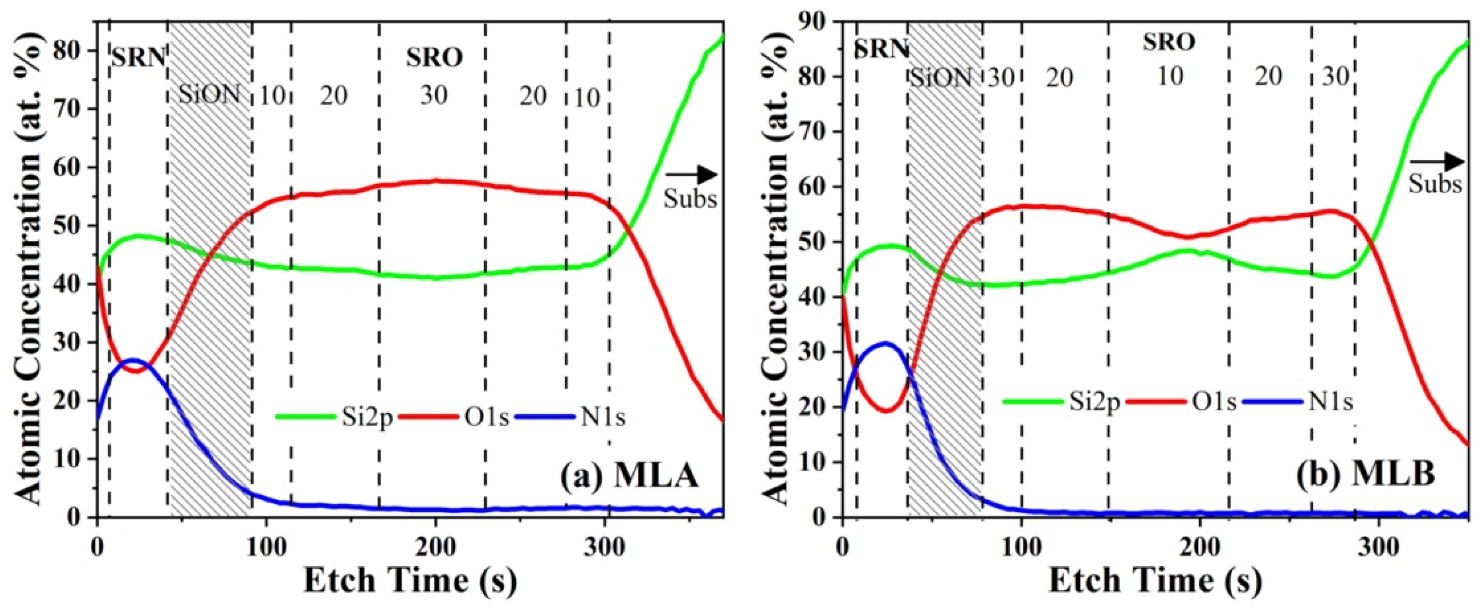
3.1. Composition
3.2. Structural Chracterization
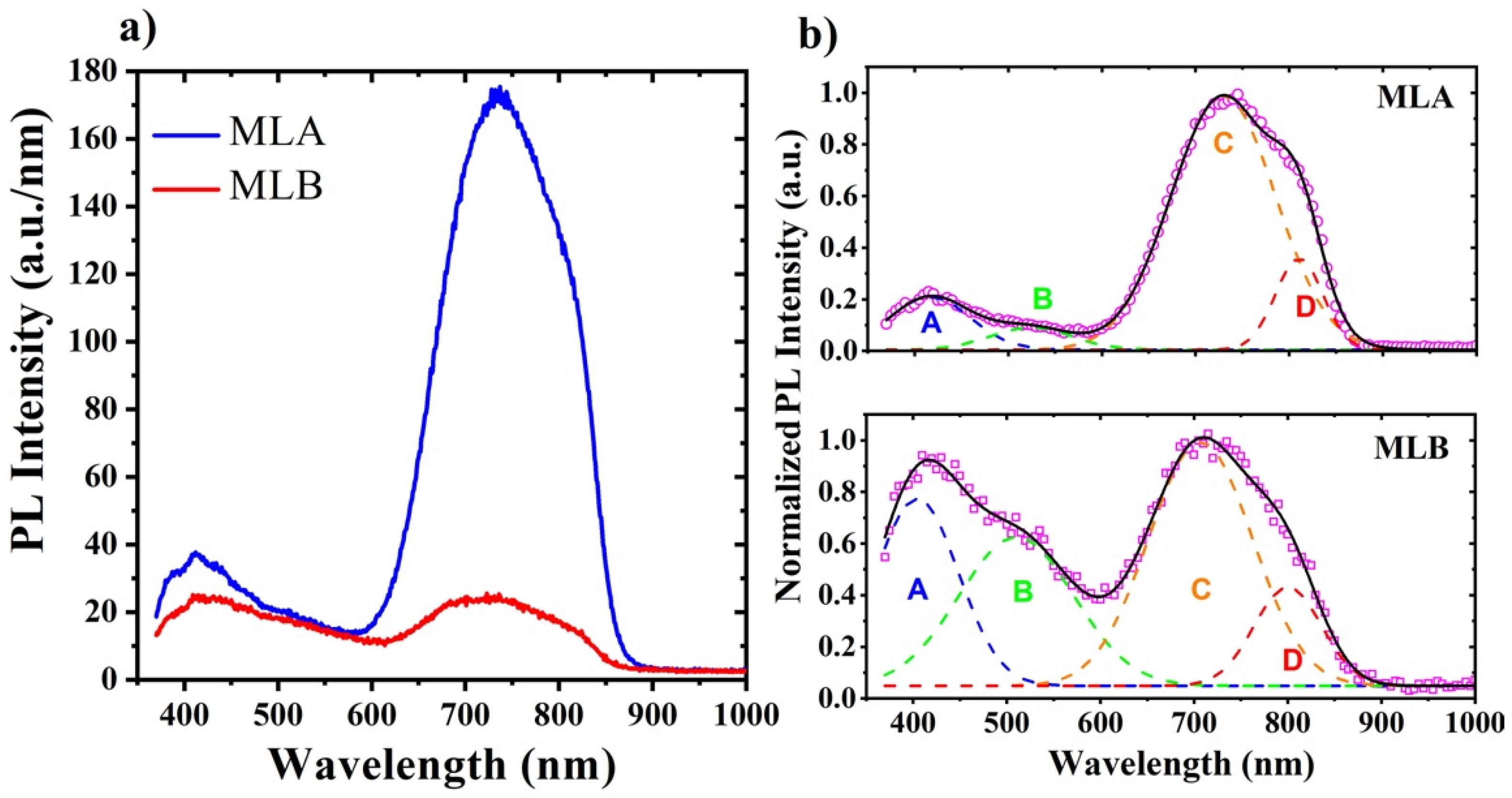
3.3. Photoluminescent Properties
4. Conclusions
Author Contributions
Funding
Institutional Review Board Statement
Informed Consent Statement
Data Availability Statement
Acknowledgments
Conflicts of Interest
References
- Walters, R.J.; Bourianoff, G.I.; Atwater, H.A. Field-Effect Electroluminescence in Silicon Nanocrystals. Nat. Mater. 2005, 4, 143–146. [Google Scholar] [CrossRef]
- Chen, L.Y.; Chen, W.H.; Hong, F.C.N. Visible Electroluminescence from Silicon Nanocrystals Embedded in Amorphous Silicon Nitride Matrix. Appl. Phys. Lett. 2005, 86, 193506. [Google Scholar] [CrossRef] [Green Version]
- Pavesi, L.; Dal Negro, L.; Mazzoleni, C.; Franzò, G.; Priolo, F. Optical Gain in Silicon Nanocrystals. Nature 2000, 408, 440–444. [Google Scholar] [CrossRef]
- Lin, G.R.; Lin, C.J.; Lin, C.K.; Chou, L.J.; Chueh, Y.L. Oxygen Defect and Si Nanocrystal Dependent White-Light and near-Infrared Electroluminescence of Si-Implanted and Plasma-Enhanced Chemical-Vapor Deposition-Grown Si-Rich SiO2. J. Appl. Phys. 2005, 97, 094306. [Google Scholar] [CrossRef] [Green Version]
- Wang, X.X.; Zhang, J.G.; Ding, L.; Cheng, B.W.; Ge, W.K.; Yu, J.Z.; Wang, Q.M. Origin and Evolution of Photoluminescence from Si Nanocrystals Embedded in a SiO2 Matrix. Phys. Rev. B Condens. Matter Mater. Phys. 2005, 72, 195313. [Google Scholar] [CrossRef] [Green Version]
- Zhou, Z.; Brus, L.; Friesner, R. Electronic Structure and Luminescence of 1.1- and 1.4-Nm Silicon Nanocrystals: Oxide Shell versus Hydrogen Passivation. Nano Lett. 2003, 3, 163–167. [Google Scholar] [CrossRef]
- Sarkar, A.; Bar, R.; Singh, S.; Chowdhury, R.K.; Bhattacharya, S.; Das, A.K.; Ray, S.K. Size-Tunable Electroluminescence Characteristics of Quantum Confined Si Nanocrystals Embedded in Si-Rich Oxide Matrix. Appl. Phys. Lett. 2020, 116, 231105. [Google Scholar] [CrossRef]
- Cheng, C.H.; Wu, C.L.; Chen, C.C.; Tsai, L.H.; Lin, Y.H.; Lin, G.R. Si-Rich SixC1-x Light-Emitting Diodes with Buried Si Quantum Dots. IEEE Photonics J. 2012, 4, 1761–1775. [Google Scholar] [CrossRef]
- Anopchenko, A.; Marconi, A.; Moser, E.; Prezioso, S.; Wang, M.; Pavesi, L.; Pucker, G.; Bellutti, P. Low-Voltage Onset of Electroluminescence in Nanocrystalline- Si/ SiO2 Multilayers. J. Appl. Phys. 2009, 106, 033104. [Google Scholar] [CrossRef]
- Marconi, A.; Anopchenko, A.; Wang, M.; Pucker, G.; Bellutti, P.; Pavesi, L. High Power Efficiency in Si-Nc/SiO2multilayer Light Emitting Devices by Bipolar Direct Tunneling. Appl. Phys. Lett. 2009, 94, 221110. [Google Scholar] [CrossRef]
- Shin, D.Y.; Park, J.H.; Kim, S.; Choi, S.H.; Kim, K.J. Graded-Size Si-Nanocrystal-Multilayer Solar Cells. J. Appl. Phys. 2012, 112, 104304. [Google Scholar] [CrossRef]
- Mehonic, A.; Buckwell, M.; Montesi, L.; Garnett, L.; Hudziak, S.; Fearn, S.; Chater, R.; McPhail, D.; Kenyon, A.J. Structural Changes and Conductance Thresholds in Metal-Free Intrinsic SiOx Resistive Random Access Memory. J. Appl. Phys. 2015, 117, 124505. [Google Scholar] [CrossRef] [Green Version]
- González-Flores, K.E.; Palacios-Márquez, B.; Alvarez-Quintana, J.; Pérez-Garcia, S.A.; Licea-Jiménez, L.; Horley, P.; Morales-Sánchez, A. Resistive Switching Control for Conductive Si-Nanocrystals Embedded in Si/SiO2 Multilayers. Nanotechnology 2018, 29, 395203. [Google Scholar] [CrossRef]
- Podhorodecki, A.; Zatryb, G.; Misiewicz, J.; Wojcik, J.; Mascher, P. Influence of the Annealing Temperature and Silicon Concentration on the Absorption and Emission Properties of Si Nanocrystals. J. Appl. Phys. 2007, 102, 043104. [Google Scholar] [CrossRef] [Green Version]
- Koch, F.; Petrova-Koch, V. Light from Si-Nanoparticle Systems—A Comprehensive View. J. Non-Cryst. Solids 1996, 198–200, 840–846. [Google Scholar] [CrossRef]
- Kohno, K.; Osaka, Y.; Toyomura, F.; Katayama, H. Photoluminescence of Si Microcrystals Embedded in SiO2 Glass Films. Jpn. J. Appl. Phys. 1994, 33, 661–662. [Google Scholar] [CrossRef]
- Kanzawa, Y.; Kageyama, T.; Takeoka, S.; Fujii, M.; Hayashi, S.; Yamamoto, K. Size-Dependent near-Infrared Photoluminescence Spectra of Si Nanocrystals Embedded in SiO2 Matrices. Solid State Commun. 1997, 102, 533–537. [Google Scholar] [CrossRef]
- Patrone, L.; Nelson, D.; Safarov, V.I.; Sentis, M.; Marine, W.; Giorgio, S. Photoluminescence of Silicon Nanoclusters with Reduced Size Dispersion Produced by Laser Ablation. J. Appl. Phys. 2000, 87, 3829–3837. [Google Scholar] [CrossRef]
- Sachenko, A.V.; Kaganovich, É.B.; Manoǐlov, É.G.; Svechnikov, S.V. Kinetics of Exciton Photoluminescence in Low-Dimensional Silicon Structures. Semiconductors 2001, 35, 1383–1389. [Google Scholar] [CrossRef]
- Kahler, U.; Hofmeister, H. Silicon Nanocrystallites in Buried SiOx Layers via Direct Wafer Bonding. Appl. Phys. Lett. 1999, 75, 641–643. [Google Scholar] [CrossRef] [Green Version]
- Rinnert, H.; Vergnat, M.; Marchal, G.; Burneau, A. Strong Visible Photoluminescence in Amorphous SiOx and SiOx: H Thin Films Prepared by Thermal Evaporation of SiO Powder. J. Lumin. 1998, 80, 445–448. [Google Scholar] [CrossRef]
- Lin, G.R.; Lin, C.J.; Lin, C.T. Low-Plasma and High-Temperature PECVD Grown Silicon-Rich SiOx Film with Enhanced Carrier Tunneling and Light Emission. Nanotechnology 2007, 18, 2–7. [Google Scholar] [CrossRef]
- Hsiao, C.Y.; Shih, C.F.; Chen, S.H.; Jiang, W.T. Comparison of Silicon Nanocrystals Embedded Silicon Oxide Films by Sputtering and PECVD. Thin Solid Film. 2011, 519, 5086–5089. [Google Scholar] [CrossRef]
- Alarcón-Salazar, J.; Zaldívar-Huerta, I.E.; Aceves-Mijares, M. Electrical and Electroluminescent Characterization of Nanometric Multilayers of SiOX/SiOY Obtained by LPCVD Including Non-Normal Emission. J. Appl. Phys. 2016, 119, 215101. [Google Scholar] [CrossRef] [Green Version]
- Dong, D.; Irene, E.A.; Young, D.R. Preparation and Some Properties of Chemically Vapor-Deposited Si-Rich SiO2 and Si3N4, Films. J. Electrochem. Soc. SOLID-STATE Sci. Technol. 1977, 125, 819–823. [Google Scholar]
- Morales, A.; Barreto, J.; Domínguez, C.; Riera, M.; Aceves, M.; Carrillo, J. Comparative Study between Silicon-Rich Oxide Films Obtained by LPCVD and PECVD. Phys. E Low-Dimens. Syst. Nanostruct. 2007, 38, 54–58. [Google Scholar] [CrossRef]
- Perálvarez, M.; Barreto, J.; Carreras, J.; Morales, A.; Navarro-Urrios, D.; Lebour, Y.; Domínguez, C.; Garrido, B. Si-Nanocrystal-Based LEDs Fabricated by Ion Implantation and Plasma-Enhanced Chemical Vapour Deposition. Nanotechnology 2009, 20, 405201. [Google Scholar] [CrossRef] [PubMed] [Green Version]
- Lai, B.H.; Cheng, C.H.; Lin, G.R. Multicolor ITO/SiOx/p-Si/Al Light Emitting Diodes with Improved Emission Efficiency by Small Si Quantum Dots. IEEE J. Quantum Electron. 2011, 47, 698–704. [Google Scholar] [CrossRef]
- Chen, K.; Ma, Z.; Huang, X.; Xu, J.; Li, W.; Sui, Y.; Mei, J.; Zhu, D. Comparison between Light Emission from Si/SiNX and Si/SiO 2 Multilayers: Role of Interface States. J. Non. Cryst. Solids 2004, 338, 448–451. [Google Scholar] [CrossRef]
- Lin, G.R.; Lin, C.K.; Chou, L.J.; Chueh, Y.L. Synthesis of Si Nanopyramids at SiOx/Si Interface for Enhancing Electroluminescence of Si-Rich SiOx. Appl. Phys. Lett. 2006, 89, 093126. [Google Scholar] [CrossRef]
- Lin, G.-R.; Lin, C.-J.; Lin, C.-K. Enhanced Fowler-Nordheim Tunneling Effect in Nanocrystallite Si Based LED with Interfacial Si Nano-Pyramids. Opt. Express 2007, 15, 2555. [Google Scholar] [CrossRef] [PubMed] [Green Version]
- Yu, Z.; Aceves-Mijares, M.; Luna-López, A.; Du, J.; Bian, D. Formation of Silicon Nanoislands on Crystalline Silicon Substrates by Thermal Annealing of Silicon Rich Oxide Deposited by Low Pressure Chemical Vapour Deposition. Nanotechnology 2006, 17, 4962–4965. [Google Scholar] [CrossRef]
- Wang, X.; Huang, R.; Song, C.; Guo, Y.; Song, J. Effect of Barrier Layers on Electroluminescence from Si/SiOxNy Multilayer Structures. J. Appl. Phys. 2013, 113, 214907. [Google Scholar] [CrossRef]
- Lin, G.R.; Pai, Y.H.; Lin, C.T.; Chen, C.C. Comparison on the Electroluminescence of Si-Rich SiNx and SiOx Based Light-Emitting Diodes. Appl. Phys. Lett. 2010, 96, 130–133. [Google Scholar] [CrossRef]
- Perálvarez, M.; Carreras, J.; Barreto, J.; Morales, A.; Domínguez, C.; Garrido, B. Efficiency and Reliability Enhancement of Silicon Nanocrystal Field-Effect Luminescence from Nitride-Oxide Gate Stacks. Appl. Phys. Lett. 2008, 92, 65–68. [Google Scholar] [CrossRef] [Green Version]
- Cabañas-Tay, S.A.; Palacios-Huerta, L.; Luna-López, J.A.; Aceves-Mijares, M.; Alcántara-Iniesta, S.; Pérez-García, S.A.; Morales-Sánchez, A. Analysis of the Luminescent Centers in Silicon Rich Silicon Nitride Light-Emitting Capacitors. Semicond. Sci. Technol. 2015, 30, 1–10. [Google Scholar] [CrossRef]
- Cabañas-Tay, S.A.; Palacios-Huerta, L.; Aceves-Mijares, M.; Coyopol, A.; Morales-Morales, F.; Pérez-García, S.A.; Licea-Jiménez, L.; Domínguez-Horna, C.; Monfil-Leyva, K.; Morales-Sánchez, A. Study of Narrow and Intense UV Electroluminescence from ITO/SRO/Si-p and ITO/SRN/SRO/Si-p Based Light Emitting Capacitors. J. Lumin. 2017, 183, 334–340. [Google Scholar] [CrossRef]
- Augustine, B.H.; Irene, E.A.; He, Y.J.; Price, K.J.; McNeil, L.E.; Christensen, K.N.; Maher, D.M. Visible Light Emission from Thin Films Containing Si, O, N, and H. J. Appl. Phys. 1995, 78, 4020–4030. [Google Scholar] [CrossRef]
- Rodríguez, J.A.; Vásquez-Agustín, M.A.; Morales-Sánchez, A.; Aceves-Mijares, M. Emission Mechanisms of Si Nanocrystals and Defects in SiO2 Materials. J. Nanomater. 2014, 2014, 1–17. [Google Scholar] [CrossRef] [Green Version]
- Robertson, J.; Powell, M.J. Gap States in Silicon Nitride. Appl. Phys. Lett. 1984, 44, 415–417. [Google Scholar] [CrossRef]
- Barbagiovanni, E.G.; Lockwood, D.J.; Rowell, N.L.; Costa Filho, R.N.; Berbezier, I.; Amiard, G.; Favre, L.; Ronda, A.; Faustini, M.; Grosso, D. Role of Quantum Confinement in Luminescence Efficiency of Group IV Nanostructures. J. Appl. Phys. 2014, 115, 044311. [Google Scholar] [CrossRef] [Green Version]
- Wu, C.L.; Lin, G.R. Power Gain Modeling of Si Quantum Dots Embedded in a SiOx Waveguide Amplifier with Inhomogeneous Broadened Spontaneous Emission. IEEE J. Sel. Top. Quantum Electron. 2013, 19, 1–9. [Google Scholar] [CrossRef]
- Jivanescu, M.; Hiller, D.; Zacharias, M.; Stesmans, A. Size Dependence of Pb-Type Photoluminescence Quenching Defects at the Si Nanocrystal Interface. EPL 2011, 96, 27003. [Google Scholar] [CrossRef]
- Hsu, Y.P.; Chang, S.J.; Su, Y.K.; Chen, S.C.; Tsai, J.M.; Lai, W.C.; Kuo, C.H.; Chang, C.S. InGaN-GaN MQW LEDs with Si Treatment. IEEE Photonics Technol. Lett. 2005, 17, 1620–1622. [Google Scholar] [CrossRef]
- Lee, C.L.; Lee, S.C.; Lee, W.I. Nonlithographic Random Masking and Regrowth of GaN Microhillocks to Improve Light-Emitting Diode Efficiency. Jpn. J. Appl. Phys. 2006, 45, L4–L7. [Google Scholar] [CrossRef]


| Label | Layer Number | RO | RN | Excess Si (at.%) | Thickness (nm) | Si-ncs | |
|---|---|---|---|---|---|---|---|
| Mean Size (nm) | Density (cm−2) | ||||||
| MLA | 1 | 10 | -- | 10.7 ± 0.6 | 10.16 ± 0.11 | 3.95 ± 0.20 | 6.79 × 10¹¹ |
| 2 | 20 | -- | 9.1 ± 0.4 | 18.89 ± 1.25 | 2.86 ± 0.81 | 9.05 × 10¹¹ | |
| 3 | 30 | -- | 8.0 ± 0.2 | 19.96 ± 0.30 | -- | -- | |
| 4 | 20 | -- | 9.1 ± 0.3 | 17.24 ± 1.55 | 2.87 ± 0.70 | 6.26 × 10¹¹ | |
| 5 | 10 | -- | 9.7 ± 0.4 | 9.67 ± 2.21 | -- | -- | |
| 6 | -- | 70 | 6.1 ± 0.2 | 13.42 ± 3.33 | -- | -- | |
| MLB | 1 | 30 | -- | 8.3 ± 0.2 | 8.15 ± 0.74 | -- | -- |
| 2 | 20 | -- | 10.8 ± 0.4 | 17.72 ± 0.93 | 2.87 ± 0.73 | 1.31 × 10¹¹ | |
| 3 | 10 | -- | 13.6 ± 1.2 | 18.80 ± 0.85 | 3.72 ± 1.03 | 9.26 × 10¹¹ | |
| 4 | 20 | -- | 9.8 ± 0.4 | 16.79 ± 0.31 | 2.89 ± 0.61 | 5.85 × 10¹¹ | |
| 5 | 30 | -- | 8.7 ± 0.1 | 8.78 ± 0.56 | -- | -- | |
| 6 | -- | 70 | 7.0 ± 0.4 | 11.51 ± 2.79 | -- | -- | |
Publisher’s Note: MDPI stays neutral with regard to jurisdictional claims in published maps and institutional affiliations. |
© 2021 by the authors. Licensee MDPI, Basel, Switzerland. This article is an open access article distributed under the terms and conditions of the Creative Commons Attribution (CC BY) license (https://creativecommons.org/licenses/by/4.0/).
Share and Cite
Avilés Bravo, J.J.; Cabañas Tay, S.A.; Palacios Huerta, L.; González Flores, K.E.; Flores Méndez, J.; Moreno Moreno, M.; Morales Sánchez, A. Effect of the Graded Silicon Content in SRN/SRO Multilayer Structures on the Si Nanocrystals and Si Nanopyramids Formation and Their Photoluminescence Response. Materials 2021, 14, 6582. https://doi.org/10.3390/ma14216582
Avilés Bravo JJ, Cabañas Tay SA, Palacios Huerta L, González Flores KE, Flores Méndez J, Moreno Moreno M, Morales Sánchez A. Effect of the Graded Silicon Content in SRN/SRO Multilayer Structures on the Si Nanocrystals and Si Nanopyramids Formation and Their Photoluminescence Response. Materials. 2021; 14(21):6582. https://doi.org/10.3390/ma14216582
Chicago/Turabian StyleAvilés Bravo, José Juan, Santiago Antonio Cabañas Tay, Liliana Palacios Huerta, Karla Esther González Flores, Javier Flores Méndez, Mario Moreno Moreno, and Alfredo Morales Sánchez. 2021. "Effect of the Graded Silicon Content in SRN/SRO Multilayer Structures on the Si Nanocrystals and Si Nanopyramids Formation and Their Photoluminescence Response" Materials 14, no. 21: 6582. https://doi.org/10.3390/ma14216582
APA StyleAvilés Bravo, J. J., Cabañas Tay, S. A., Palacios Huerta, L., González Flores, K. E., Flores Méndez, J., Moreno Moreno, M., & Morales Sánchez, A. (2021). Effect of the Graded Silicon Content in SRN/SRO Multilayer Structures on the Si Nanocrystals and Si Nanopyramids Formation and Their Photoluminescence Response. Materials, 14(21), 6582. https://doi.org/10.3390/ma14216582