
Extensive Analysis on the Effects of Post-Deposition Annealing for ALD-Deposited Al2O3 on an n-Type Silicon Substrate


Abstract
1. Introduction
2. Methods and Materials
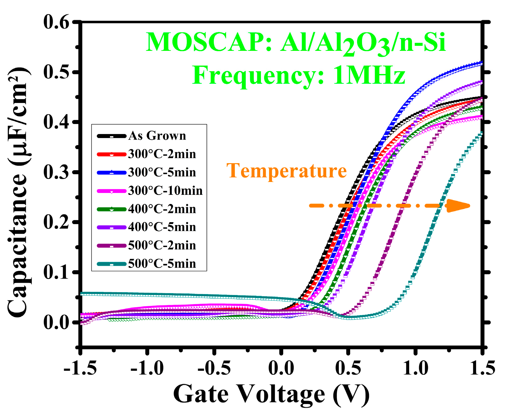
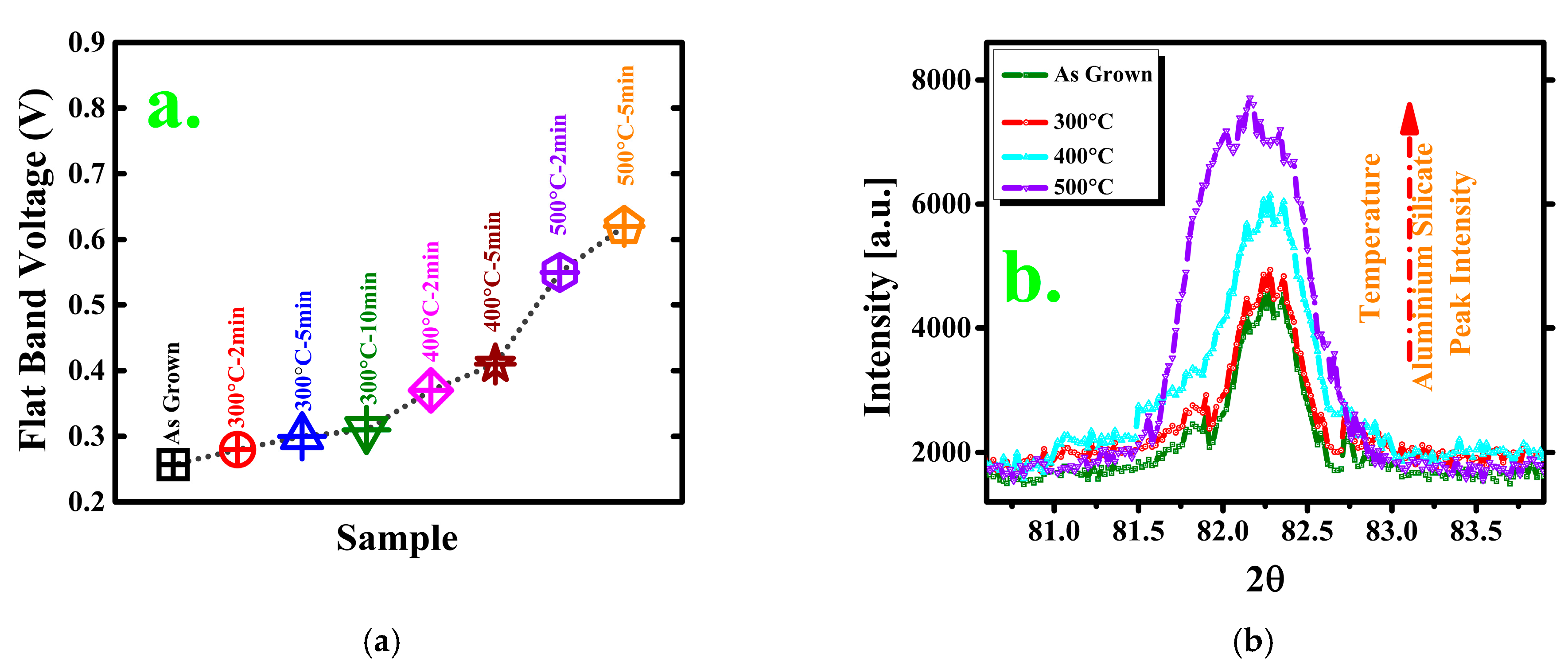
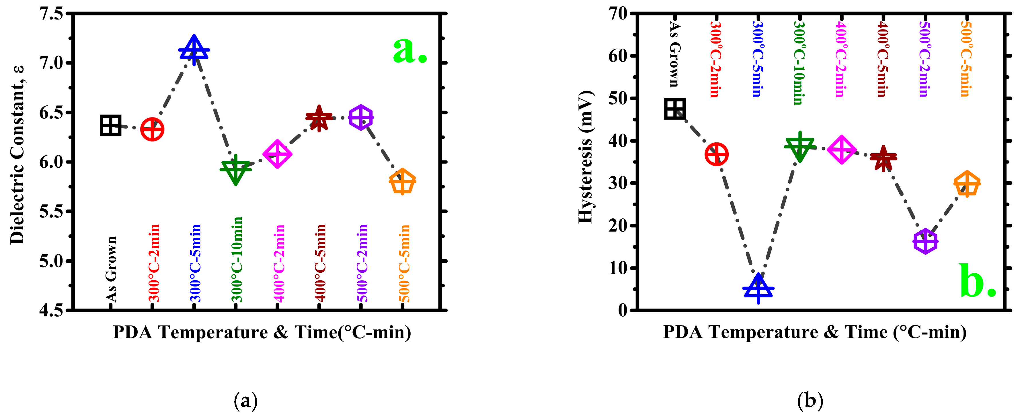
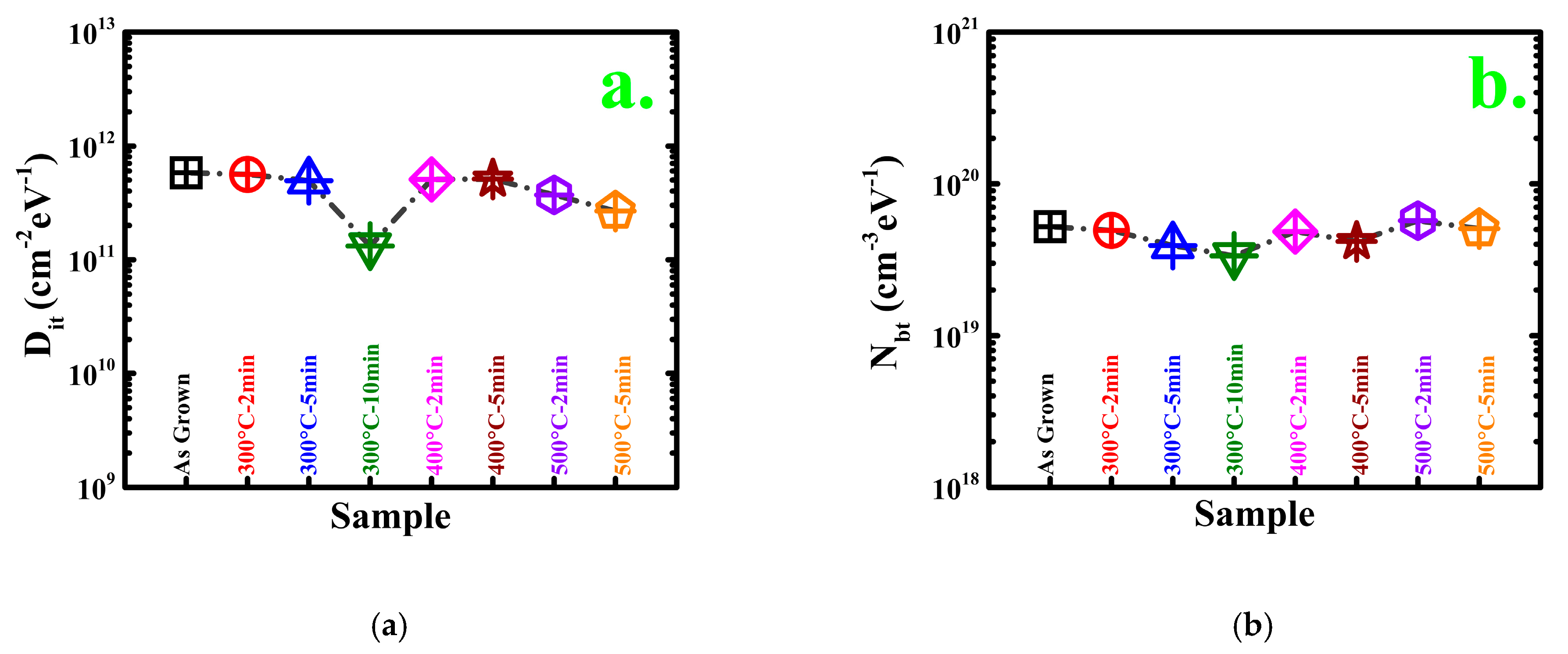
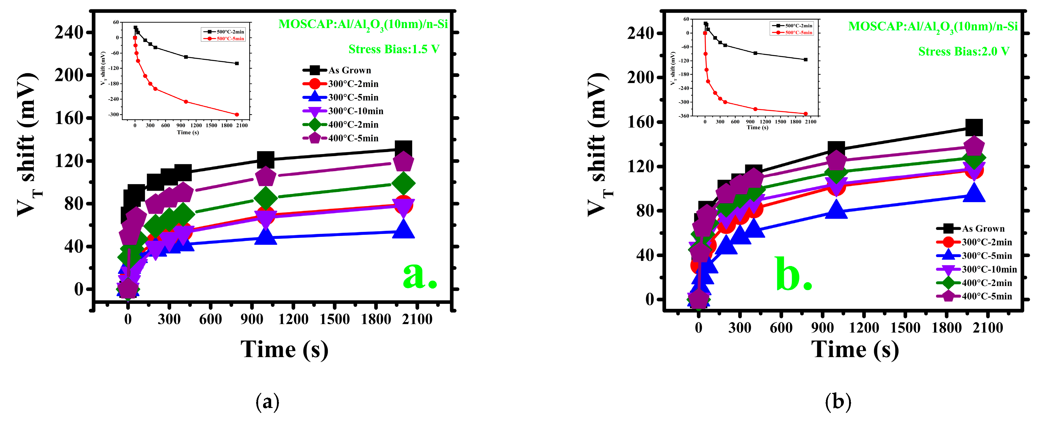
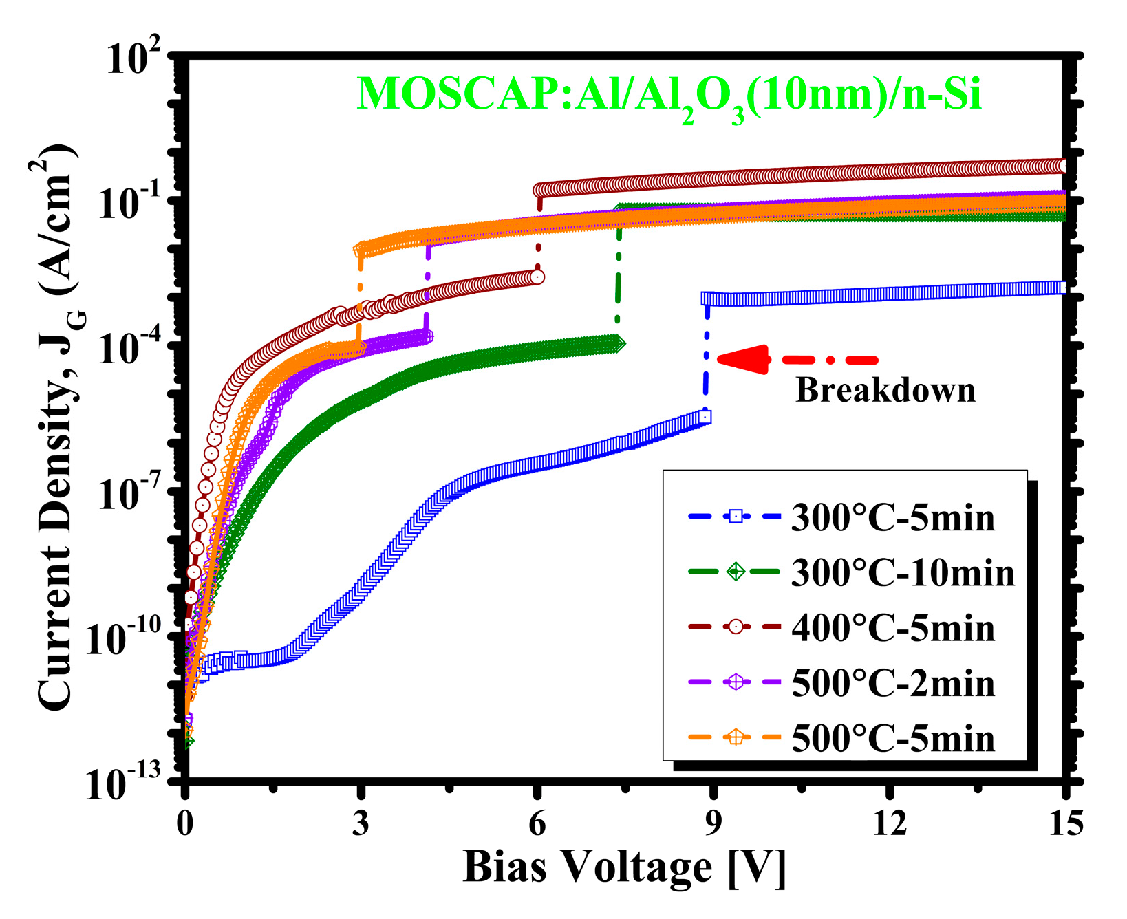
3. Results and Discussion
4. Conclusions
Author Contributions
Funding
Institutional Review Board Statement
Informed Consent Statement
Data Availability Statement
Conflicts of Interest
References
- del Alamo, J.A. Nanometre-scale electronics with III–V compound semiconductors. Nature 2011, 479, 317. [Google Scholar] [CrossRef] [PubMed]
- Heyns, M.; Alian, A.; Brammertz, G.; Caymax, M.; Chang, Y.C.; Chu, L.K.; De Jaeger, B.; Eneman, G.; Gencarelli, F.; Groeseneken, G.; et al. Advancing CMOS beyond the Si roadmap with Ge and III/V devices. In Proceedings of the 2011 International Electron Devices Meeting, Washington, DC, USA, 5–7 December 2011; Volume 3, pp. 13.1.1–13.1.4. [Google Scholar]
- Kamata, Y. High-k/Ge MOSFETs for future nanoelectronics. Mater. Today 2008, 11, 30–38. [Google Scholar] [CrossRef]
- Ye, P.D. Main determinants for III–V metal-oxide-semiconductor field-effect transistors (invited). J. Vac. Sci. Technol. A 2008, 26, 697–704. [Google Scholar] [CrossRef]
- Robertson, J.; Falabretti, B. Band offsets of high K gate oxides on high mobility semiconductors. Mater. Sci. Eng. B 2006, 135, 267–271. [Google Scholar] [CrossRef]
- Xuan, Y.; Wu, Y.Q.; Shen, T.; Yang, T.; Ye, P.D. High performance submicron inversion-type enhancement-mode InGaAs MOSFETs with ALD Al2O3, HfO2 and HfAlO as gate dielectrics. In Proceedings of the 2007 IEEE International Electron Devices Meeting, Washington, DC, USA, 10–12 December 2007; pp. 637–640. [Google Scholar]
- Lin, J.Q.; Lee, S.J.; Oh, H.J.; Lo, G.Q.; Kwong, D.L.; Chi, D.Z. Inversion-mode self-aligned In0.53Ga0.47 As N-channel metal-oxide-semiconductor field-effect transistor with HfAlO gate dielectric and TaN metal gate. IEEE Electron. Device Lett. 2008, 29, 977–980. [Google Scholar] [CrossRef]
- Goel, N.; Heh, D.; Koveshnikov, S.; Ok, I.; Oktyabrsky, S.; Tokranov, V.; Kambhampatic, R.; Yakimov, M.; Sun, Y.; Pianetta, P.; et al. Addressing The Gate Stack Challenge For High Mobility InxGa1-xAs Channels For NFETs. In Proceedings of the 2008 IEEE International Electron Devices Meeting, San Francisco, CA, USA, 15–17 December 2008; pp. 1–4. [Google Scholar]
- Zadeh, D.H.; Oomine, H.; Suzuki, Y.; Kakushima, K.; Ahmet, P.; Nohira, H.; Kataoka, Y.; Nishiyama, A.; Sugii, N.; Tsutsui, K.; et al. La2O3/In0.53Ga0.47As metal-oxide-semiconductor capacitor with low interface state density using TiN/W gate electrode. Solid-State Electron. 2013, 82, 29–33. [Google Scholar] [CrossRef]
- Chobpattana, V.; Mates, T.E.; Zhang, J.Y.; Stemmer, S. Scaled ZrO2 dielectrics for In0.53Ga0.47As gate stacks with low interface trap densities. Appl. Phys. Lett. 2014, 104, 182912. [Google Scholar] [CrossRef]
- Albertin, K.F.; Valle, M.A.; Pereyra, I. Study of TiO2 and SiO2/TiO2 as Gate Dielectric Maaterials. ECS Trans. 2007, 4, 409–416. [Google Scholar] [CrossRef]
- Koo, J.; Lee, J.; Kim, S.; Do Kim, Y.; Jeon, H.; Kim, D.S.; Kim, Y. Characteristics of hafnium-aluminum-oxide thin films deposited by using atomic layer deposition with various aluminum compositions. J. Korean Phys. Soc. 2005, 47, 501–507. [Google Scholar]
- Rahman, M.M.; Kim, J.-G.; Kim, D.-H.; Kim, T.-W. Characterization of Al Incorporation into HfO2 Dielectric by Atomic Layer Deposition. Micromachines 2019, 10, 361. [Google Scholar] [CrossRef]
- Wilk, G.D.; Muller, D.A. Correlation of annealing effects on local electronic structure and macroscopic electrical properties for HfO2 deposited by atomic layer deposition. Appl. Phys. Lett. 2003, 83, 3984–3986. [Google Scholar] [CrossRef]
- Yun, M.; Kim, M.S.; Ko, Y.D.; Moon, T.H.; Hong, J.H.; Myoung, J.M.; Yun, I. Effects of post-metallization annealing of high-K dielectric thin films grown by MOMBE. Microelectron. Eng. 2005, 77, 48–54. [Google Scholar] [CrossRef]
- Hashizume, T.; Kaneki, S.; Oyobiki, T.; Ando, Y.; Sasaki, S. Effects of postmetallization annealing on interface properties of Al2O3/GaN structures. Appl. Phys. Express 2018, 11, 124102. [Google Scholar] [CrossRef]
- Thesis, M.; Kuriyama, A.; Ohmi, S.I.; Tsutsui, K.; Iwai, H. Effect of Post Metallization Annealing for La2O3 Gate Thin Film. Jpn. J. Appl. Phys. 2005, 44, 1045–1051. [Google Scholar]
- Benick, J.; Richter, A.; Li, T.A.; Grant, N.E.; Mcintosh, K.R.; Ren, Y.; Weber, K.J.; Hermle, M.; Glunz, S.W. Effect of a post-deposition anneal on Al2O3/Si interface properties. In Proceedings of the 2010 35th IEEE Photovoltaic Specialists Conference, Honolulu, HI, USA, 20–25 June 2010; pp. 891–896. [Google Scholar]
- Gonullu, M.P.; Ates, H. The characteristic evolution of TiO2/Al2O3 bilayer films produced by ALD: Effect of substrate type and wide range annealing temperature. Superlattices Microstruct. 2020, 142, 106529. [Google Scholar] [CrossRef]
- Przewlocki, H.M.; Gutt, T.; Piskorski, K. The inflection point of the capacitance- voltage, C(VG), characteristic and the flat- band voltage of metal-oxide-semiconductor structures. J. Appl. Phys. 2014, 115, 204510. [Google Scholar] [CrossRef]
- Wang, W.; Akiyama, K.; Mizubayashi, W.; Nabatame, T.; Ota, H.; Toriumi, A. Effect of Al-diffusion-induced positive flatband voltage shift on the electrical characteristics of Al-incorporated high- k metal-oxide-semiconductor field-effective transistor. J. Appl. Phys. 2009, 105, 064108. [Google Scholar] [CrossRef]
- Wang, W.; Mizubayashi, W.; Akiyama, K.; Nabatame, T.; Toriumi, A. Systematic investigation on anomalous positive Vfb shift in Al-incorporated high-k gate stacks. Appl. Phys. Lett. 2008, 92, 1–4. [Google Scholar] [CrossRef]
- Dueñas, S.; Castán, H.; García, H.; Gómez, A.; Bailón, L.; Kukli, K.; Aarik, J.; Ritala, M.; Leskelä, M. Comparative Study of Flatband Voltage Transients on High-k Dielectric-Based Metal–Insulator–Semiconductor Capacitors. J. Electrochem. Soc. 2008, 155, G241. [Google Scholar] [CrossRef]
- Cho, M.-H.; Rho, Y.S.; Choi, H.-J.; Nam, S.W.; Ko, D.-H.; Ku, J.H.; Kang, H.C.; Noh, D.Y.; Whang, C.N.; Jeong, K. Annealing effects of aluminum silicate films grown on Si(100). J. Vac. Sci. Technol. A Vac. Surf. Film. 2002, 20, 865–872. [Google Scholar] [CrossRef]
- Callister, W.D.; Rethwisch, D.G. Materials Science and Engineering: An Introduction; Wiley: New York, NY, USA, 2018; Available online: https://www.wiley.com/en-us/Materials+Science+and+Engineering%3A+An+Introduction%2C+10th+Edition-p-9781119405498 (accessed on 2 March 2021).
- Engel-Herbert, R.; Hwang, Y.; Stemmer, S. Comparison of methods to quantify interface trap densities at dielectric/III-V semiconductor interfaces. J. Appl. Phys. 2010, 108, 124101. [Google Scholar] [CrossRef]
- Lin, J.; Monaghan, S.; Cherkaoui, K.; Povey, I.M.; Sheehan, B.; Hurley, P.K. Examining the relationship between capacitance-voltage hysteresis and accumulation frequency dispersion in InGaAs metal-oxide-semiconductor structures based on the response to post-metal annealing. Microelectron. Eng. 2017, 178, 204–208. [Google Scholar] [CrossRef]
- Tang, K.; Winter, R.; Zhang, L.; Droopad, R.; Eizenberg, M.; Mcintyre, P.C. Border trap reduction in Al2O3/InGaAs gate stacks. Appl. Phys. Lett. 2015, 107, 202102. [Google Scholar] [CrossRef]
- Rahman, M.; Kim, D.; Kim, T. Border Trap Characterizations of Al2O3/ZrO2 and Al2O3/HfO2 Bilayer Films Based on Ambient Post Metal Annealing and Constant Voltage Stress. Nanomaterials 2020, 10, 527. [Google Scholar] [CrossRef]
- Rahman, M.M.; Kim, J.-G.; Kim, D.-H.; Kim, T.-W. Border Trap Extraction with Capacitance- Equivalent Thickness to Reflect the Quantum Mechanical Effect on Atomic Layer Deposition High-k/In0.53Ga0.47As on 300-mm Si Substrate. Sci. Rep. 2019, 9, 9861. [Google Scholar] [CrossRef]
- Rahman, M.M.; Kim, J.G.; Kim, D.H.; Kim, T.W. Comparison of the interface and border traps of nanolaminate and bilayer structures of Al2O3 and HfO2 on In0.53Ga0.47As. Jpn. J. Appl. Phys. 2019, 58, 120905. [Google Scholar] [CrossRef]
- Kim, D.; Kim, T.; Amir, W. Comprehensive Analysis of Quantum Mechanical Effects of Interface Trap and Border Trap on a 300-mm Si Substrate. IEEE Access 2020, 8, 211464–211473. [Google Scholar]
- Winter, R.; Ahn, J.; McIntyre, P.C.; Eizenberg, M. New method for determining flat-band voltage in high mobility semiconductors. J. Vac. Sci. Technol. B Nanotechnol. Microelectron. Mater. Process. Meas. Phenom. 2013, 31, 030604. [Google Scholar] [CrossRef]
- Khalil, O.M.; Mingareev, I.; Bonhoff, T.; El-Sherif, A.F.; Richardson, M.C.; Harith, M.A. Studying the effect of zeolite inclusion in aluminum alloy on measurement of its surface hardness using laser-induced breakdown spectroscopy technique. Opt. Eng. 2014, 53, 014106. [Google Scholar] [CrossRef]
- Atuanya, C.U.; Ibhadode, A.O.A.; Dagwa, I.M. Effects of breadfruit seed hull ash on the microstructures and properties of Al-Si-Fe alloy/breadfruit seed hull ash particulate composites. Results Phys. 2012, 2, 142–149. [Google Scholar] [CrossRef]
- Ma, P.; Jia, Y.; Prashanth, K.G.; Yu, Z.; Li, C.; Zhao, J.; Yang, S.; Huang, L. Effect of Si content on the microstructure and properties of Al-Si alloys fabricated using hot extrusion. J. Mater. Res. 2017, 32, 2210–2217. [Google Scholar] [CrossRef]
- Yuan, Y.; Yu, B.; Ahn, J.; McIntyre, P.C.; Asbeck, P.M.; Rodwell, M.J.W.; Taur, Y. A distributed bulk-oxide trap model for Al2O3 InGaAs MOS devices. IEEE Trans. Electron Devices 2012, 59, 2100–2106. [Google Scholar] [CrossRef]
- Sereni, G.; Vandelli, L.; Larcher, L.; Morassi, L.; Veksler, D.; Bersuker, G. A new method for extracting interface state and border trap densities in high-k/III-V MOSFETs. In Proceedings of the 2014 IEEE International Reliability Physics Symposium, Waikoloa, HI, USA, 1–5 June 2014; pp. 4–9. [Google Scholar]
- Wang, J.; Farrokh-Baroughi, M.; Shanmugam, M.; Samadzadeh-Tarighat, R.; Sivoththaman, S.; Paul, S. Passivation of silicon surfaces using atomic layer deposited metal oxides. Mater. Res. Soc. Symp. Proc. 2009, 1153, 147–152. [Google Scholar] [CrossRef]
- Birner, S. The nextnano software for the simulation of semiconductor heterostructures. Topol. Nanodevice Model. 2019. Available online: https://www.nextnano.de/downloads/publications/abstracts/Abstract_TopologicalNanodeviceModeling_2014_Delft_Birner.pdf (accessed on 5 March 2021).


| ALD | RTA | Thermal Evaporator | |||||
|---|---|---|---|---|---|---|---|
| Sample | Oxide | Cycle | Temperature | Gas | Temperature | Time (min) | Metal Layer |
| As-grown | Al2O3 | 100 | 250 | Ar | - | - | Al |
| 300 °C–2 min | 100 | 250 | Ar | 300 °C | 2 | ||
| 300 °C–5 min | 100 | 250 | Ar | 300 °C | 5 | ||
| 300 °C–10 min | 100 | 250 | Ar | 300 °C | 10 | ||
| 400 °C–2 min | 100 | 250 | Ar | 400 °C | 2 | ||
| 400 °C–5 min | 100 | 250 | Ar | 400 °C | 5 | ||
| 500 °C–2 min | 100 | 250 | Ar | 500 °C | 2 | ||
| 500 °C–5 min | 100 | 250 | Ar | 500 °C | 5 | ||
| As-Grown | 300 °C–2 min | 300 °C–5 min | 300 °C–10 min | 400 °C–2 min | 400 °C–5 min | 500 °C–2 min | 500 °C–5 min | |
|---|---|---|---|---|---|---|---|---|
| Test 1 | 0.46 | 0.47 | 0.54 | 0.43 | 0.42 | 0.47 | 0.45 | 0.48 |
| Test 2 | 0.38 | 0.52 | 0.53 | 0.45 | 0.45 | 0.47 | 0.53 | 0.52 |
| Test 3 | 0.375 | 0.34 | 0.53 | 0.43 | 0.42 | 0.51 | 0.52 | 0.46 |
| Test 4 | 0.48 | 0.46 | 0.53 | 0.38 | 0.51 | 0.50 | 0.43 | 0.29 |
| Test 5 | 0.475 | 0.4 | 0.53 | 0.46 | 0.43 | 0.46 | 0.54 | 0.52 |
| Test 6 | 0.375 | 0.35 | 0.56 | 0.40 | 0.44 | 0.44 | 0.48 | 0.27 |
| Test 7 | 0.45 | 0.45 | 0.475 | 0.48 | 0.50 | 0.52 | 0.475 | 0.425 |
| Avg | 0.43 | 0.43 | 0.53 | 0.43 | 0.45 | 0.48 | 0.49 | 0.42 |
| STD | 0.05 | 0.07 | 0.03 | 0.03 | 0.04 | 0.03 | 0.04 | 0.1 |
| As-Grown | 300 °C–2 min | 300 °C–5 min | 300 °C–10 min | 400 °C–2 min | 400 °C–5 min | 500 °C–2 min | 500 °C–5 min | |
|---|---|---|---|---|---|---|---|---|
| Test 1 | 30.0 | 13.6 | 10.9 | 17.6 | 42.0 | 33.4 | 9.0 | 13.2 |
| Test 2 | 55.5 | 31.3 | 2.2 | 40.7 | 56.6 | 58.2 | 14.6 | 22.2 |
| Test 3 | 55.6 | 36.8 | 8.2 | 34.1 | 32.1 | 36.5 | 26.5 | 76.2 |
| Test 4 | 53.7 | 6.1 | 2.4 | 54.3 | 28.1 | 28.7 | 2.5 | 9.4 |
| Test 5 | 52.6 | 62.9 | 1.9 | 65.0 | 23.5 | 27.0 | 33.7 | 15.7 |
| Test 6 | 51.1 | 36.8 | 0.4 | 33.5 | 49.0 | 44.5 | 3.9 | 10.4 |
| Test 7 | 34.3 | 70.7 | 10.4 | 27.2 | 34.0 | 22.3 | 24.1 | 61.8 |
| Avg | 47.5 | 36.9 | 5.2 | 38.6 | 37.9 | 35.8 | 16.3 | 29.8 |
| STD | 10.7 | 23.6 | 4.5 | 16.1 | 11.8 | 12.2 | 12.0 | 27.4 |
Publisher’s Note: MDPI stays neutral with regard to jurisdictional claims in published maps and institutional affiliations. |
© 2021 by the authors. Licensee MDPI, Basel, Switzerland. This article is an open access article distributed under the terms and conditions of the Creative Commons Attribution (CC BY) license (https://creativecommons.org/licenses/by/4.0/).
Share and Cite
Bhattacharjee, A.; Kim, T.-W. Extensive Analysis on the Effects of Post-Deposition Annealing for ALD-Deposited Al2O3 on an n-Type Silicon Substrate. Materials 2021, 14, 3328. https://doi.org/10.3390/ma14123328
Bhattacharjee A, Kim T-W. Extensive Analysis on the Effects of Post-Deposition Annealing for ALD-Deposited Al2O3 on an n-Type Silicon Substrate. Materials. 2021; 14(12):3328. https://doi.org/10.3390/ma14123328
Chicago/Turabian StyleBhattacharjee, Atish, and Tae-Woo Kim. 2021. "Extensive Analysis on the Effects of Post-Deposition Annealing for ALD-Deposited Al2O3 on an n-Type Silicon Substrate" Materials 14, no. 12: 3328. https://doi.org/10.3390/ma14123328
APA StyleBhattacharjee, A., & Kim, T.-W. (2021). Extensive Analysis on the Effects of Post-Deposition Annealing for ALD-Deposited Al2O3 on an n-Type Silicon Substrate. Materials, 14(12), 3328. https://doi.org/10.3390/ma14123328